

Page 1
Data Sheet No. PD60259
IRS2453D(S)PbF
SELF-OSCILLATING FULL-BRIDGE DRIVER IC
Features
CT, RT programmable oscillator
Logic level latched shutdown pin
Non-latched shutdown on CT pin (1/6th V
Description
The IRS2453D is based on the popular IR2153 self-oscillating
half-bridge gate driver IC, and incorporates a high voltage fullbridge gate driver with a front end oscillator similar to the
industry standard CMOS 555 timer. HVIC and latch immune
CMOS technologies enable ruggedized monolithic construction.
The output driver features a high pulse current buffer stage
designed for minimum driver cross-conduction. Noise immunity
is achieved with low di/dt peak of the gate drivers, and with a
undervoltage lockout hysteresis greater than 1.5 V. The
IRS2453D also includes latched and non-latched shutdown pins.
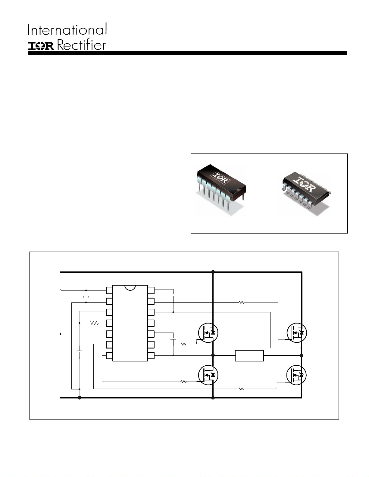
Typical Connection Diagram
Integrated 600 V full-bridge gate driver
15.6V Zener clamp on
Micropower startup
+ AC rectified line
V
CC
)
CC
Internal bootstrap FETs
Excellent latch immunity on all inputs & outputs
ESD protection on all pins
14-lead SOIC or PDIP package
1.0 µs (typ.) internal deadtime
Packages
14 Lead PDIP 14 Lead SOIC (Narrow Body)
IRS2453DPbF IRS2453DSPbF
15 V
VCC
1
COM
2
VB1
HO1
14
13
D
CT
3
RT
4
SD
5
LO1
6
LO2
7
- AC rectified line
3
5
4
2
S
R
I
VS1
NC
VB2
HO2
VS2
12
11
10
9
8
LOAD
1
Page 2
IRS2453DPbF
Absolute Maximum Ratings
Absolute maximum ratings indicate sustained limits beyond which damage to the device may occur. All voltage parameters
are absolute voltages referenced to COM, all currents are defined positive into any lead. The thermal resistance and power
dissipation ratings are measured under board mounted and still air conditions.
Parameter
Symbol Definition Min. Max. Units
V
V
V
V
dVS/dt
B1, VB2
S1, VS2
, V
HO1
, V
LO1
High side floating supply voltage -0.3 625
High side floating supply offset voltage
High side floating output voltage
HO2
Low side output voltage -0.3
LO2
VRT RT pin voltage
VCT CT pin voltage
VSD
SD pin voltage -0.3
IRT RT pin current
ICC
Supply current (Note 1) --- 25
Allowable offset voltage slew rate -50 50 V/ns
PD
PD
R
R
TS
θJA
θJA
TJ
TL
Maximum power dissipation @ T
Maximum power dissipation @ T
Thermal resistance, junction to ambient, 8-Pin DIP --- 125
Thermal resistance, junction to ambient, 8-Pin SOIC --- 200
≤ +25 ºC, 8-Pin DIP
A
≤ +25 ºC, 8-Pin SOIC
A
Junction temperature -55 150
Storage temperature -55 150
Lead temperature (soldering, 10 seconds) --- 300
VB - 25 VB + 0.3
V
- 0.3 VB + 0.3
S
V
+ 0.3
CC
-0.3
-0.3
VCC + 0.3
VCC + 0.3
VCC + 0.3
-5 5
--- 1.0
--- 0.625
V
mA
W
ºC/W
ºC
Note 1:
This IC contains a zener clamp structure between the chip V
and COM which has a nominal
CC
breakdown voltage of 15.6 V. Please note that this supply pin should not be driven by a DC, low
impedance power source greater than the V
specified in the Electrical Characteristics section.
CLAMP
2
Page 3
IRS2453DPbF
Recommended Operating Conditions
For proper operation the device should be used within the recommended conditions.
Parameter
Symbol Definition Min. Max. Units
V
BS1, VBS2
VS1, VS2
VCC
Note 2:
Note 3:
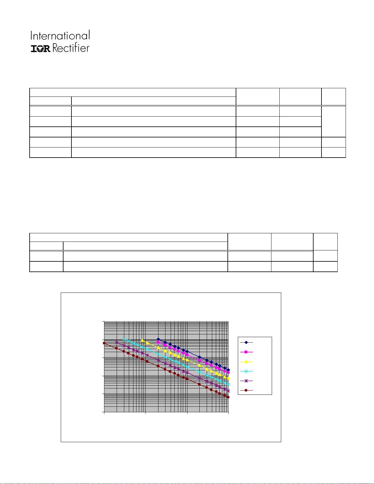
Recommended Component Values
Symbol Component Min. Max. Units
RT
CT CT pin capacitor value
High side floating supply voltage
Steady state high side floating supply offset voltage -3.0 (Note 2) 600
Supply voltage V
ICC
TJ
Supply current (Note 3) 5 mA
Junction temperature -25 125 ºC
Care should be taken to avoid output switching conditions where the V
ground by more than 5 V.
Enough current should be supplied to the
pin of the IC to keep the internal 15.6 V zener diode
V
CC
clamping the voltage at this pin.
Parameter
Timing resistor value 1
VBIAS (V
CC, VBS) = 14 V, VS=0 V and TA = 25 °C, CLO1=CLO2 = CHO1=CHO2 = 1 nF.
V
- 0.7 V
CC
CCUV+
node flies inductively below
S
V
---
CLAMP
CLAMP
kΩ
330 --- pF
V
1000000
100000
10000
Frequency (Hz)
IRS2453 D Fre quenc y vs. RT
1000
100
10
1000 10000 100000 1000000
RT (O h m)
CT Values
330pf
470pF
1nF
2.2nF
4.7nF
10nF
3
Page 4
IRS2453DPbF
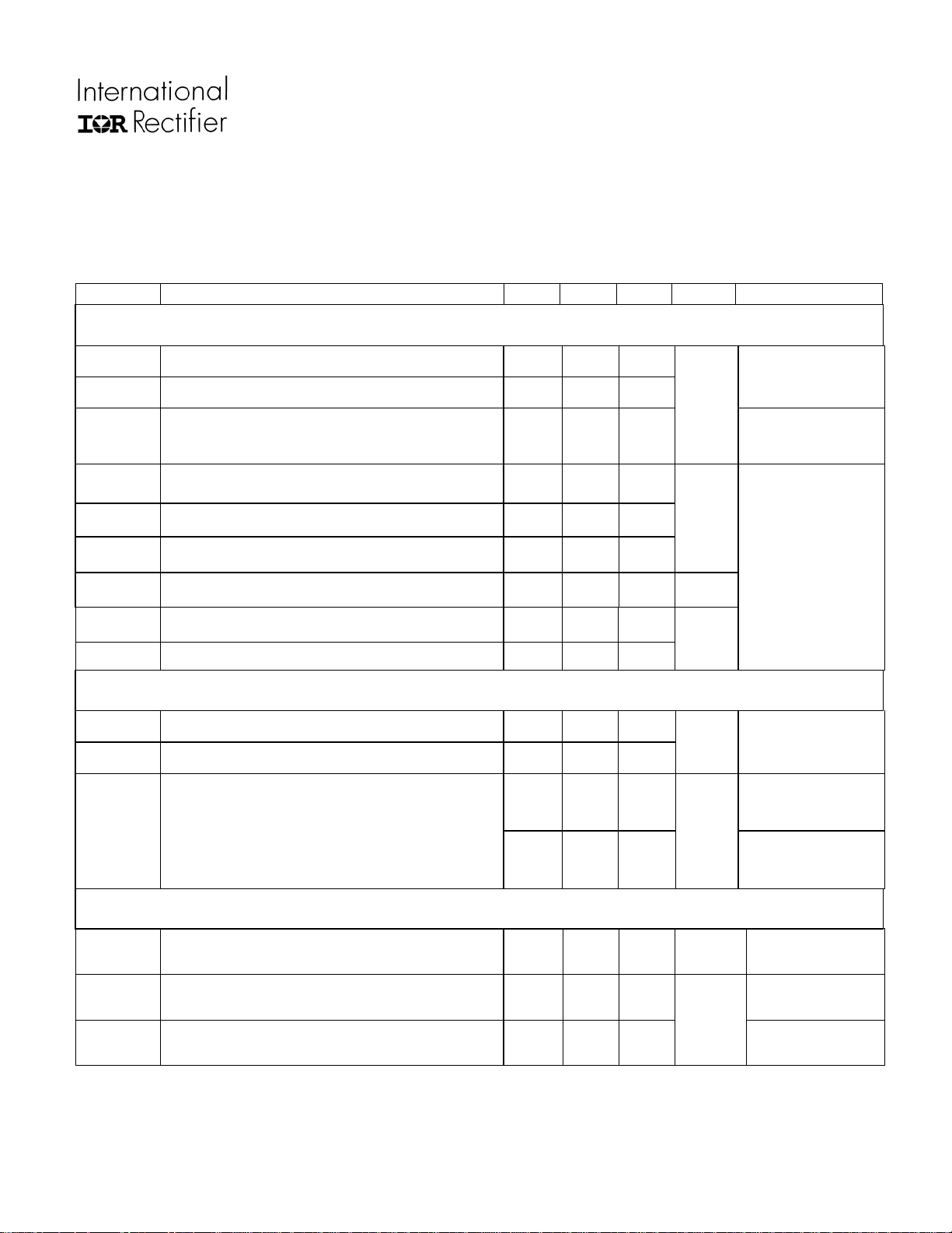
Electrical Characteristics
V
(VCC, VBS) = 14 V, CT = 1 nF and TA = 25 °C unless otherwise specified. The VO and IO parameters are referenced to COM and are
BIAS
applicable to the respective output leads: HO or LO. CLO1=CLO2=CHO1=CHO2=1 nF.
Symbol Definition Min Typ Max Units
Low Voltage Supply Characteristics
V
Rising VCC undervoltage lockout threshold 10.0 11.0 12.0
+
CCUV
V
Falling VCC undervoltage lockout threshold 8.0 9.0 10.0
-
CCUV
V
CCUVHYS
I
QCCUV
VCC undervoltage lockout hysteresis 1.5 2.0 2.4
Micropower startup V
supply current --- 140 200 µA
CC
IQCC Quiescent VCC supply current --- 1.3 2.0
I
VCC supply current at f
CC_20K
I
VCC supply current when SD > VSD --- 360 500 µA
CCFLT
V
VCC Zener clamp voltage 14.6 15.6 16.6 V ICC = 5 mA
CLAMP
(RT = 36.5 kΩ) --- 3.0 3.5
osc
Floating Supply Characteristics
I
QBS1UV,
I
QBS2UV
I
QBS1,
I
QBS2
V
BS1UV+,
V
BS2UV+
V
BS1UV-,
V
BS2UV-,
I
LK1, ILK2
Micropower startup V
supply current
BS
--- 3 10
Quiescent V
supply current
BS
--- 30 100
supply undervoltage positive going
V
BS
threshold
supply undervoltage negative going
V
BS
threshold
Offset supply leakage current --- --- 50
8.0 9.0 10.0
7.0 8.0 9.0
V
mA
µA
V
µA
Test Conditions
V
≤ V
CC
V
≤ V
CC
V
CC
VB = VS = 600 V
CCUV-
CCUV-
= VBS
,
Oscillator I/O Characteristics
f
OSC
Oscillator frequency
19.6
88
20.2 20.8
94 100
d RT pin duty cycle 48 50 52 %
ICT CT pin current --- 0.05 1.0
I
UV-mode CT pin pulldown current 1 5 --- mA
CTUV
V
Upper CT ramp voltage threshold --- 9.3 ---
CT+
V
Lower CT ramp voltage threshold --- 4.7 ---
CT-
V
High level RT output voltage, VCC - VRT
RT+
V
Low level RT output voltage
RT-
V
UV-mode RT output voltage
RTUV
--- 10 50 I
--- 100 300 I
--- 10 50 I
--- 100 300 I
--- 0 100
kHz
µA
V
mV
R
= 36.5 kΩ
T
R
= 7.15 kΩ
T
fo < 100 kHz
VCC = 7 V
RT = 100 µA
RT = 1 mA
RT = 100 µA
RT = 1 mA
V
≤ V
CC
CCUV-
4
Page 5
IRS2453DPbF
Electrical Characteristics
V
(VCC, VBS) = 14 V, CT = 1 nF and TA = 25 °C unless otherwise specified. The VO and IO parameters are referenced to COM and are
BIAS
applicable to the respective output leads: HO or LO. CLO1=CLO2=CHO1=CHO2=1 nF.
Symbol Definition Min Typ Max Units
Gate Driver Output Characteristics
VOH High level output voltage, V
VOL Low level output voltage, VO
V
UV-mode output voltage, VO
OL_UV
tr
tf
tsd
td
Output rise time --- 120 200
Output fall time --- 50 100
Shutdown propagation delay --- 250 ---
Output deadtime (HO or LO) 0.8 1.0 1.40
BIAS
- VO
--- V
---
CC
--- COM ---
--- COM ---
V
ns
µs
Test Conditions
≤ V
,
CCUV-
I
V
CC
I
O = 0 A
O = 0 A
IO+ Output source current --- 180 ---
IO- Output sink current --- 260 ---
Shutdown
VSD
V
CTSD
Shutdown threshold at SD pin (latched)
CT voltage shutdown threshold (non latched)
1.8 2.0 2.3
2.2 2.3 2.5
--- 10 50
V
SD mode RT output voltage, VCC - VRT
RTSD
--- 100 300
Bootstrap FET Characteristics
V
B1_ON
V
B2_ON
I
B1_CAP
I
B2_CAP
I
B1_10 V
I
B2_10 V
VB when the bootstrap FET is on 13.7 14.0 --- V
VB source current when FET is on 40 55 --- C
VB source current when FET is on 10 12 ---
mA
V
mV
mA
I
RT = 100 µA,
VCT = 0 V
I
RT = 1 mA,
VCT = 0 V
=0.1 µF
BS
VB=10 V
5
Page 6

IRS2453DPbF
Lead Assignment
VCC
1
COM
2
CT
3
D
3
VB1
HO1
VS1
14
13
12
5
RT
4
4
NC
11
2
SD
5
LO1
6
LO2
7
Lead Definitions
Pin Symbol Description
1 VCC Logic and internal gate drive supply voltage
2 COM IC power and signal ground
3 CT Oscillator timing capacitor input
4 RT Oscillator timing resistor input
5 SD Shutdown input
6 LO1 Low side gate driver output
7 LO2 Low side gate driver output
8 VS2 High voltage floating supply return
9 HO2 High side gate driver output
10 VB1 High side gate driver floating supply
11 NC No connect
12 VS1 High voltage floating supply return
13 HO1 High side gate driver output
14 VB1 High side gate driver floating supply
S
R
I
Lead
VB2
HO2
VS2
10
9
8
6
Page 7

Functional Block Diagram
4
RT
IRS2453DPbF
14
VB1
SD
CT
R
+
-
R
RQ
+
S
-
R/2
+
R/2
DETECT
-
UV
3
5
2.0V
S
R1
R2
S
R
DEAD
TIME
Q
DEAD
TIME
Q
Q
Q
PULSE
GEN
PULSE
GEN
Level
HV
Level
Shift
HV
Shift
DELAY
DELAY
PULSE
FILTER
BOOTSTRAP
DRIVE
PULSE
FILTER
BOOTSTRAP
DRIVE
Q
R
S
Q
R
S
15.4V
HO1
13
12
VS1
LO1
6
10
VB2
9
HO2
8
VS2
VCC
1
LO2
7
2
COM
All values are typical.
7
Page 8

IRS2453DPbF
Timing Diagram
VCCUV+
VCC
2/3 VCC
1/3 VCC
1/6 VCC
VCC
LO1
VCC
LO2
Fault mode
VCT<1/6*VCC
DT
HO1
HO2
VRT
IRT
VCC
VCC
VCC
1mA
-1mA
DT
DT
8
Page 9

IRS2453DPbF
Functional Description
Under-Voltage Lock-Out Mode (UVLO)
The under-voltage lockout mode (UVLO) is defined as the state
the IC is in when V
IRS2453D under-voltage lock-out is designed to maintain an ultra
low supply current of less than 150 µA, and to guarantee the IC is
fully functional before the high and low side output drivers are
activated. During under-voltage lock-out mode, the high and low
side driver outputs LO1, LO2, HO1, HO2 are all low. With V
above the V
to oscillate.
CCUV+
Normal Operating Mode
Once VCC reaches the start-up threshold V
opens, RT increases to approximately V
external CT capacitor starts charging. Once the CT voltage
reaches V
resistor ladder, LO1 and HO2 turn on with a delay equivalent to
the deadtime (t
(approximately 2/3 of V
to approximately ground (V
discharging and the deadtime circuit is activated. At the end of
the deadtime, LO2 and HO1 go high. Once the CT voltage
reaches V
deadtime is activated. At the end of the deadtime, LO1 and HO2
go high and the cycle starts over again.
The frequency is best determined by the graph, Frequency vs.
RT, page 3, for different values of CT. A first order approximate of
the oscillator frequency can also be calculated by the following
formula::
This equation can vary slightly from actual measurements due to
internal comparator over- and under-shoot delays.
CT-
CT-
is below the turn-on threshold of the IC. The
CC
threshold, the IC turns on and the output begin
, the MOSFET M1
CCUV+
(VCC-V
CC
(about 1/3 of VCC), established by an internal
). Once the CT voltage reaches V
d
), LO1 and HO2 go low, RT goes down
CC
, LO2 and HO1 go low, RT goes to high again, the
f
≈
), the CT capacitor starts
RT-
1
453.1
CTRT
××
) and the
RT+
Latched Shutdown
When the SD pin is brought above 2 V, the IC goes into fault
mode and all outputs are low. V
to restart the IC. The SD pin can be used for over-current
V
CCUV-
or over-voltage protection using appropriate external circuitry.
has to be recycled below
CC
50%
CC
HO1
td_HO1
LO1
50%
Deadtime Waveform Definitions
50%
td_LO1
50%
ton_LO
Deadtime Waveform
CT+
tr tf
90%
HO
LO
10%
Rise and Fall Time Waveform
Bootstrap MOSFET
The internal bootstrap FET and supply capacitor (C
comprise the supply voltage for the high side driver circuitry. The
internal boostrap FET only turns on when the corresponding LO
is high. To guarantee that the high-side supply is charged up
before the first pulse on HO1 and HO2, LO1 and LO2 are both on
when CT ramps between zero and 1/3*V
also on when CT is grounded below 1/6*V
bootstrap capacitor is charged when CT is brought back over
.
1/3*V
CC
. LO1 and LO2 are
CC
to ensure that the
CC
BOOT
)
Non-Latched Shutdown
If CT is pulled down below
an external circuit, CT doesn’t charge up and oscillation stops. All
outputs are held low and the bootstrap FETs are off. Oscillation
will resume once CT is able to charge up again to V
(approximately 1/6 of VCC) by
V
CTSD
CT-
.
50%
9
Page 10

IRS2453DPbF
IRS2453D
IRS2453DS
10
Page 11

E
N
IRS2453DPbF
LOADED TAPE FEED DIRECTION
B
F
OTE : CONTROLLING
DIMENSION IN MM
CARRIER TAPE DIMENSION FOR 14SOICN
Metric Imperial
Code Min Max Min Max
A 7.90 8.10 0.311 0.318
B 3.90 4.10 0.153 0.161
C 15.70 16.30 0.618 0.641
D 7.40 7.60 0.291 0.299
E 6.40 6.60 0.252 0.260
F 9.40 9.60 0.370 0.378
G 1.50 n/a 0.059 n/a
H 1.50 1.60 0.059 0.062
F
C
E
G
H
REEL DIMENSIONS FOR 14SOICN
Metric Imperial
Code Min Max Min Max
A 329.60 330.25 12.976 13.001
B 20.95 21.45 0.824 0.844
C 12.80 13.20 0.503 0.519
D 1.95 2.45 0.767 0.096
E 98.00 102.00 3.858 4.015
F n/a 22.40 n/a 0.881
G 18.50 21.10 0.728 0.830
H 16.40 18.40 0.645 0.724
A
A
G
B
D
H
D
C
A
11
Page 12

IRS2453DPbF
Part number
Date code
Pin 1
Identifier
?
P
MARKING CODE
Lead Free Released
Non-Lead Free
Released
IRxxxxxx
YWW?
?XXXX
Lot Code
(Prod mode - 4 digit SPN code)
Assembly site code
Per SCOP 200-002
ORDER INFORMATION
14-lead PDIP IRS2453DPbF
14-lead SOIC IRS2453DSPbF
14-lead SOIC tape & reel IRS2453DSTRPbF
IR logo
This product has been designed and qualified for the industrial level.
Qualification standards can be found at www.irf.com <http://www.irf.com/>
IR WORLD HEADQUARTERS: 233 Kansas St., El Segundo, California 90245 Tel: (310) 252-7105
Data and specifications subject to change without notice. 6/26/2006
The SOIC-14 is MSL3 qualified.
12
Page 13

IRS2453DPbF
February 20, 2006
July ‘05 revision Feb ‘06 revision
Symbol Definition Min Typ Max Min Typ Max Units
Supply Characteristics
+
V
V
V
Rising VCC undervoltage lockout
CCUV
-
V
Falling VCC undervoltage lockout
CCUV
CCUVHYS
VCC Zener clamp voltage
CLAMP
Oscillator I/O Characteristics
f
OSC
REVISION HISTORY
threshold
threshold
V
undervoltage lockout hysteresis
CC
10.0 11.0 12.0
7.8 8.8 9.8
0.5 1.0 1.5
14.9 15.9 16.9
Oscillator frequency (RT=36.5 kΩ) 18.6 19.2 19.8 19.6 20.2 20.8
Oscillator frequency (R
=7.15 kΩ) 85 91 97 89 95 101
T
10.0 11.0 12.0
8.0 9.0 10.0
1.6 2.0 2.4
14.6 15.6 16.6
V
kHz
V
CT+
Upper C
ramp voltage threshold
T
--- 9.33 ---
--- 9.1 --V
V
CT-
tr
IO+
Lower C
ramp voltage threshold
T
Output rise time
Output source current
--- 4.66 ---
--- 100 150
--- 200 --- --- 180 ---
--- 4.8 ---
--- 120 220
ns
mA
IO-
Output sink current
--- 400 --- --- 260 ---
Bootstrap FET Characteristics
V
B1_ON
V
B2_ON
I
B1_CAP
I
B2_CAP
I
B1_10 V
I
B2_10 V
VB when the bootstrap FET is on --- 14 --- --- 13.7 --- V
VB source current when FET is on --- 50 --- 30 55 ---
VB source current when FET is on --- 10 --- 8 12 ---
mA
13
Page 14

IRS2453DPbF
June 30, 2006
June ’06 revision Feb ’06 revision
Symbol Definition Min Typ Max Min Typ Max Units
Supply Characteristics
V
CCUVHYS
I
CC_20K VCC
I
CCFLT
I
QBS1,
I
QBS2
Oscillator I/O Characteristics
f
OSC
V
CT+
V
CT-
V
undervoltage lockout hysteresis
CC
supply current at f
OSC
(RT = 36.5 kΩ)
1.5 2.0 2.4
--- 3.0 3.5
VCC supply current when SD>VSD --- 360 500 Not specified
Quiescent V
Oscillator frequency (R
Upper C
Lower C
BS
ramp voltage threshold
T
ramp voltage threshold
T
supply current
=7.15 kΩ) 88 94 100 89 95 101 kHz
T
--- 30 100
--- 9.3 ---
--- 4.7 ---
1.6 2.0 2.4 V
Not specified mA
--- 60 100
--- 9.1 ---
--- 4.8 ---
µA
V
tr
Output rise time
--- 120 200 --- 120 220
Gate Driver Output Characteristics
td
Output deadtime (HO or LO) 0.8 1.0 1.40
0.75 1.0 1.50
tsd Shutdown propagation delay --- 250 --- --- 275 ---
Shutdown Characteristics
Shutdown threshold at SD pin
(latched)
C
voltage shutdown threshold (non
T
latched)
1.8 2.0 2.3 --- 2.0 ---
2.2 2.3 2.5
--- 2.3 ---
V
VSD
CTSD
Bootstrap FET Characteristics
V
B1_ON
V
B2_ON
I
B1_CAP
I
B2_CAP
I
B1_10 V
I
B2_10 V
VB when the bootstrap FET is on 13.7 14.0 --- --- 13.7 --- V
VB source current when FET is on 40 55 --- 30 55 ---
VB source current when FET is on 10 12 --- 8 12 ---
ns
µs
V
mA
14
 Loading...