

Page 1
查询IRS20124S供应商
DIGITAL AUDIO DRIVER WITH DISCRETE DEAD-TIME AND PROTECTION
Data Sheet No. PD60240 revA
IRS20124S(PbF)
Features
• 200V high voltage ratings deliver up to 1000W
output power in Class D audio amplifier
applications
• Integrated dead-time generation and bi-directional
over current sensing simplify design
• Programmable compensated preset dead-time for
improved THD performances over temperature
• High noise immunity
• Shutdown function protects devices from overload
conditions
• Operates up to 1MHz
• 3.3V/5V logic compatible input
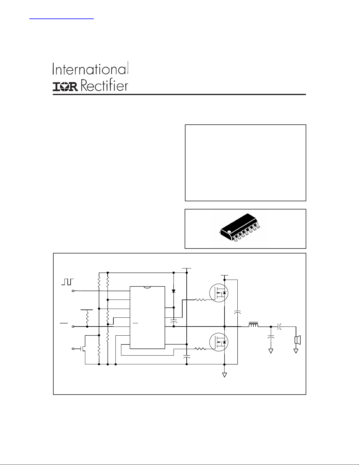
Typical Application Diagram
Product Summary
V
SUPPLY
IO+/- 1A / 1.2A typ.
Selectable Dead Time
Prop Delay Time 70ns typ.
Bi-directional Over
Current Sensing
200V max.
15/25/35/45ns typ.
Package
<20V
<200V
14-Lead SOIC
IN
<20V
OC
SD
www.irf.com 1
IN
OCSET1
DT/SD
OCSET2
OC
COM
LO
IRS20124
V
NC
NC
VB
HO
VS
NC
CC
Page 2
IRS20124S(PbF)
Description
The IRS20124S is a high voltage, high speed power MOSFET driver with internal dead-time and shutdown
functions specially designed for Class D audio amplifier applications.
The internal dead time generation block provides accurate gate switch timing and enables tight dead-time
settings for better THD performances.
In order to maximize other audio performance characteristics, all switching times are designed for immunity
from external disturbances such as VCC perturbation and incoming switching noise on the DT pin. Logic
inputs are compatible with LSTTL output or standard CMOS down to 3.0V without speed degradation. The
output drivers feature high current buffers capable of sourcing 1.0A and sinking 1.2A. Internal delays are
optimized to achieve minimal dead-time variations. Proprietary HVIC and latch immune CMOS technologies
guarantee operation down to Vs= –4V, providing outstanding capabilities of latch and surge immunities with
rugged monolithic construction.
Absolute Maximum Ratings
Absolute maximum ratings indicate sustained limits beyond which damage to the device may occur. All voltage parameters
are absolute voltages referenced to COM. All currents are defined positive into any lead. The thermal resistance and power
dissipation ratings are measured under board mounted and still air conditions.
Symbol Definition Min. Max. Units
V
B
V
s
V
HO
V
CC
V
LO
V
IN
V
OC
V
OCSET1
V
OCSET2
dVs/dt Allowable Vs voltage slew rate - 50 V/ns
Pd Maximum power dissipation - 1.25 W
Rth
JA
T
J
T
S
T
L
2 www.irf.com
High side floating supply voltage -0.3 220 V
High side floating supply voltage VB-20 VB+0.3 V
High side floating output voltage Vs-0.3 VB+0.3 V
Low side fixed supply voltage -0.3 20 V
Low side output voltage -0.3 Vcc+0.3 V
Input voltage -0.3 Vcc+0.3 V
OC pin input voltage -0.3 Vcc+0.3 V
OCSET1 pin input voltage -0.3 Vcc+0.3 V
OCSET2 pin input voltage -0.3 Vcc+0.3 V
Thermal resistance, Junction to ambient - 100 °C/W
Junction Temperature - 150 °C
Storage Temperature -55 150 °C
Lead temperature (Soldering, 10 seconds) - 300 °C
Page 3
IRS20124S(PbF)
Recommended Operating Conditions
For Proper operation, the device should be used within the recommended conditions. The Vs and COM
offset ratings are tested with all supplies biased at 15V differential.
Symbol Definition Min. Max. Units
V
B
V
S
V
HO
V
CC
V
LO
V
IN
V
OC
V
OCSET1
V
OCSET2
T
A
Note 1: Logic operational for VS equal to -8V to 200V. Logic state held for VS equal to -8V to -VBS.
Dynamic Electrical Characteristics
V
(VCC, VBS) = 15V, CL = 1nF and TA = 25°C unless otherwise specified. Figure 2 shows the timing definitions.
BIAS
High side floating supply absolute voltage Vs+10 Vs+18 V
High side floating supply offset voltage Note 1 200 V
High side floating output voltage Vs V
B
Low side fixed supply voltage 10 1 8 V
Low side output voltage 0 VCC V
Logic input voltage 0 VCC V
OC pin input voltage 0 VCC V
OCSET1 pin input voltage 0 VCC V
OCSET2 pin input voltage 0 VCC V
Ambient Temperature -40 125 °C
V
Symbol Definition Min. Typ. Max. Units Test Conditions
t
on
t
off
t
t
tsd Shutdown propagation delay — 140 200
toc Propagation delay time from Vs>Vsoc+ to OC — 2 8 0 — OC
twoc min OC pulse width — 100 —
toc filt OC input filter time — 200 —
DT1 Deadtime: LO turn-off to HO turn-on (DT
DT2 Deadtime: LO turn-off to HO turn-on (DT
DT3 Deadtime: LO turn-off to HO turn-on (DT
DT4 Deadtime: LO turn-off to HO turn-on (DT
& HO turn-off to LO turn-on (DT
www.irf.com 3
High & low side turn-on propagation delay — 60 80
High & low side turn-off propagation delay — 60 80
Turn-on rise time — 25 40
r
Turn-off fall time — 15 35
f
)
LO-HO
& HO turn-off to LO turn-on (DT
& HO turn-off to LO turn-on (DT
& HO turn-off to LO turn-on (DT
) 0 15 40 VDT>V
HO-LO
)
LO-HO
) 5 2 5 50 V
HO-LO
)
LO-HO
) 10 35 60 V
HO-LO
)
LO-HO
T= V
HO-LO)VD
15 45 70 V
DT4
nsec
VS=0V
VS=200V
SET1
OC
SET2
DT1>VDT
DT2>VDT
DT3>VDT
=3.22V
=1.20V
DT1
> V
DT2
> V
DT3
> V
DT4
Page 4

IRS20124S(PbF)
Static Electrical Characteristics
V
(VCC, VBS) = 15V and TA = 25°C unless otherwise specified.
BIAS
Symbol Definition Min. Typ. Max. Units Test Conditions
UV
UV
UV
UV
V
V
V
V
V
OH
V
OL
I
QBS
I
QCC
I
LK
I
IN+
I
IN-
I
o+
I
o-
V
DT1
V
DT2
V
DT3
V
DT4
SOC+
SOC-
Logic high input voltage 2.5 — — Vcc=10~20V
IH
Logic low input voltage — — 1.2
IL
High level output voltage, V
Low level output voltage, V
Vcc supply UVLO positive threshold 8.3 9.0 9.7
CC+
Vcc supply UVLO negative threshold 7.5 8.2 8.9
CC-
High side well UVLO positive threshold 8.3 9.0 9.7
BS+
High side well UVLO negative threshold 7.5 8.2 8.9
BS-
High side quiescent current — — 1
Low side quiescent current — — 4 VDT =V
BIAS
O
– V
— — 1.2 Io=0A
O
— — 0.1 Io=0A
V
mA
High to Low side leakage current — — 50 VB=VS =200V
Logic “1” input bias current — 3 10 VIN =3.3V
µA
Logic “0” input bias current — 0 1.0 VIN =0V
Output high short circuit current (Source) — 1. 0 — Vo=0V, PW<10µS
Output low short circuit current (Sink) — 1.2 — Vo=15V, PW<10µS
A
DT mode select threshold 1 0.8xVcc 0.89xVcc 0.97xVcc
DT mode select threshold 2 0.51xVcc 0.57xVcc 0.63xVcc
DT mode select threshold 3 0.32xVcc 0.36xVcc 0.40xVcc
DT mode select threshold 4 0.21xVcc 0.23xVcc 0.25xVcc
Positive OC threshold in Vs 0.75 1.0 1.25 OC
V
OC
Negative OC threshold in Vs -1.25 -1.0 -0.75 OC
OC
SET1
SET
SET1
SET2
cc
=3.22V
2=1.20
=3.22V
=1.20V
4 www.irf.com
Page 5
IRS20124S(PbF)
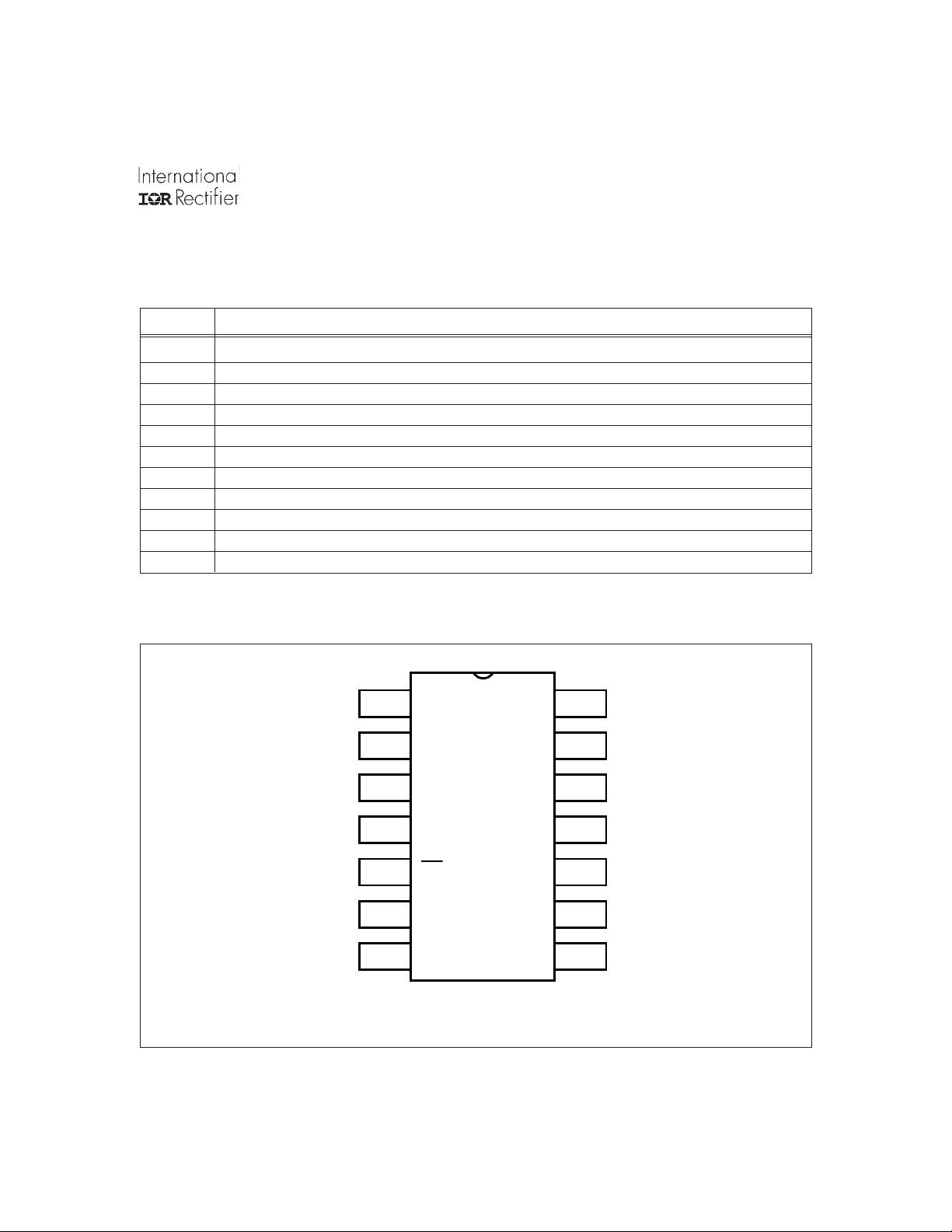
Lead Definitions
Symbol Description
VCC Low side logic Supply voltage
VB High side floating supply
HO High side output
VS High side floating supply return
IN Logic input for high and low side gate driver outputs (HO and LO), in phase with HO
DT/SD Input for programmable dead-time, referenced to COM. Shutdown LO and HO when tied to COM
COM Low side supply return
LO Low side output
OC Over current output (negative logic)
OC
OC
SET1
SET2
Input for setting negative over current threshold
Input for setting positive over current threshold
VB
VS
CC
14
13
12
11
10
9
8
1
IN
2
OCSET1
3
DT/SD
OCSET2
4
5
OC
6
COM
7
LO
IR20124S 14 Lead SOIC (narrow body)
www.irf.com 5
NC
NC
HO
NC
V
Page 6
IRS20124S(PbF)
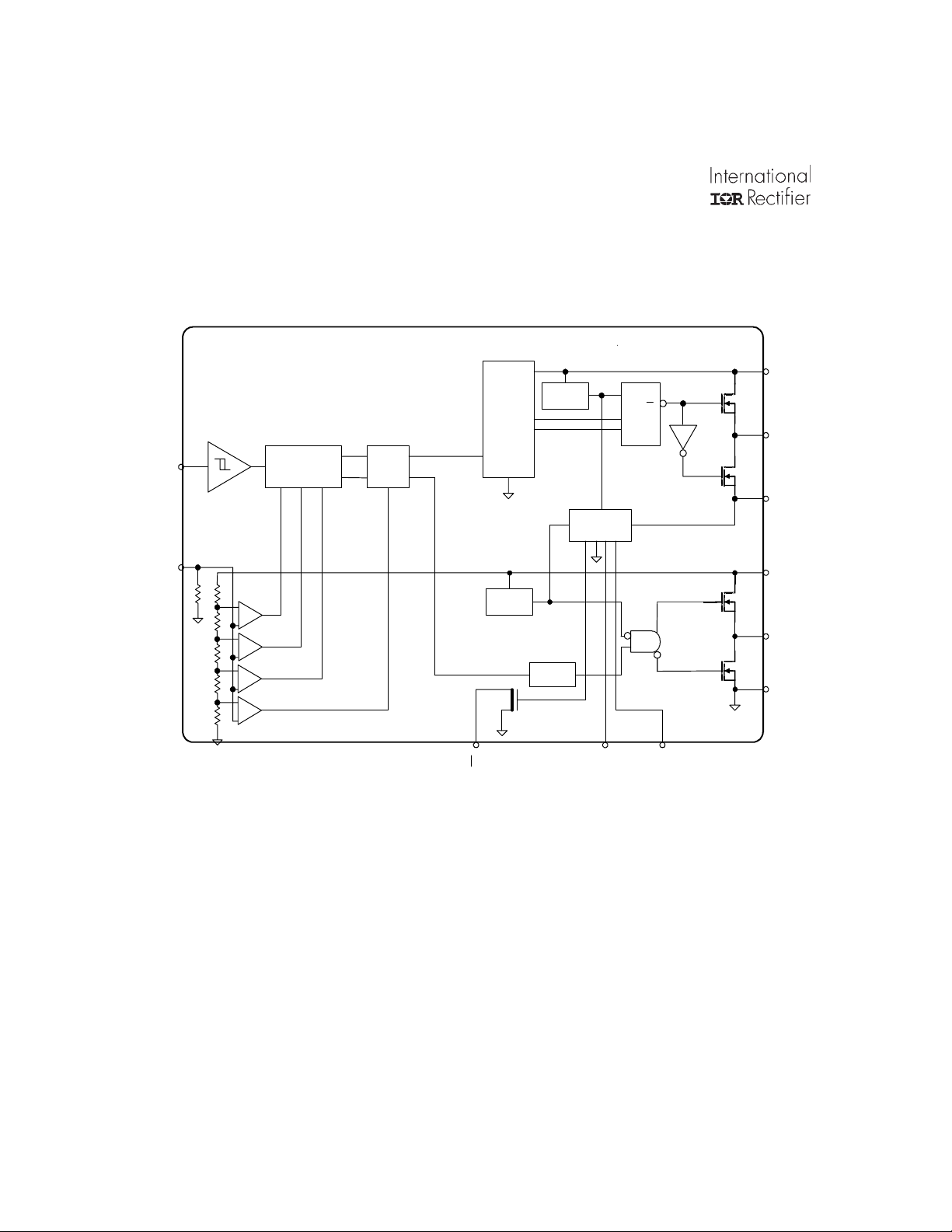
Block Diagram
DT/SD
UV
UV
DETECT
DELAY
CURRENT
SENSIN G
LEVEL
SHIFTER
IN
DEAD
TIME
SD
DETECT
OC
UV
Q
S
R
2
T
E
S
OCSET1
C
O
VB
HO
VS
Vcc
LO
COM
6 www.irf.com
Page 7
IRS20124S(PbF)
IN
HO
LO
50% 50%
t
on(L)
t
off(H)
90%
DT
HO-LO
10%
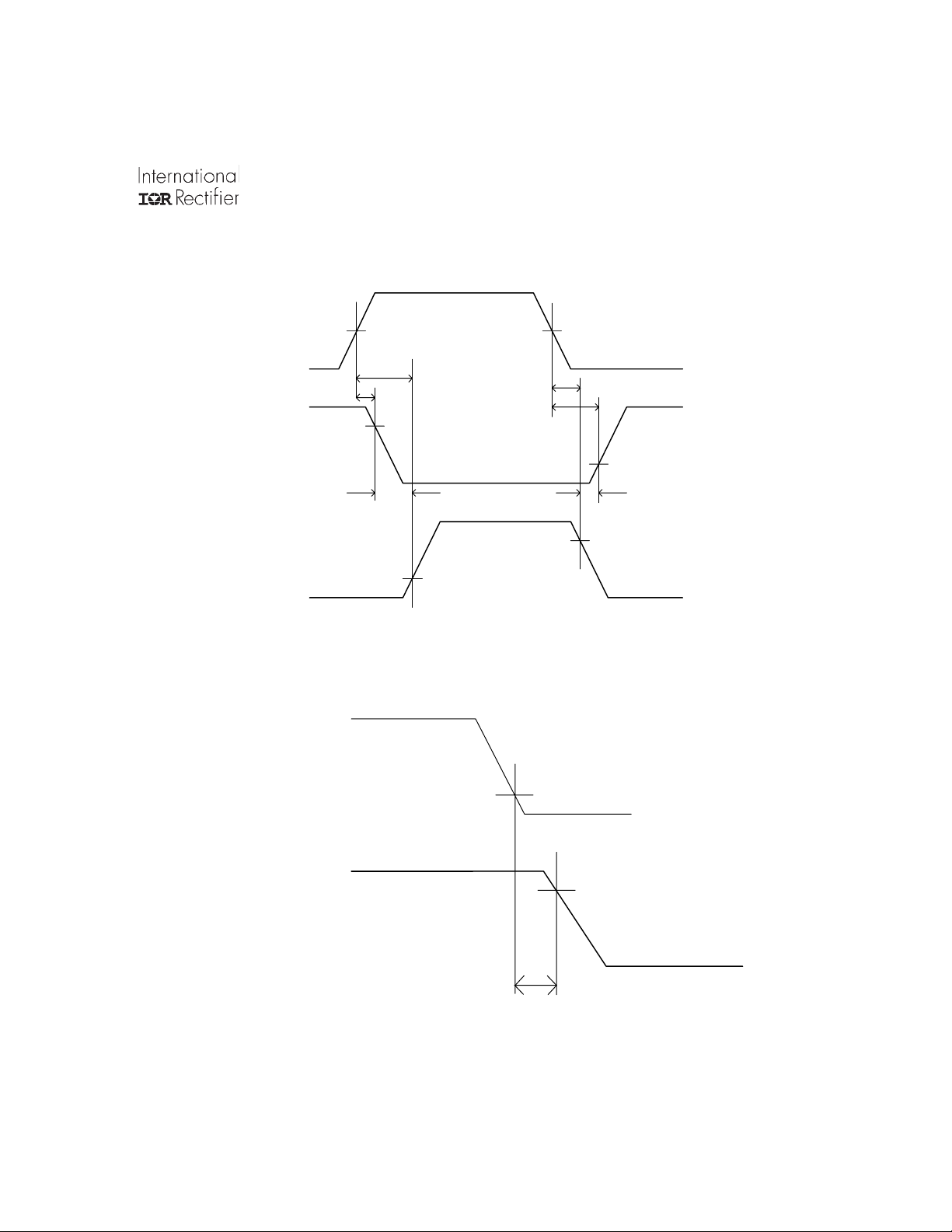
Figure 1. Switching Time Waveform Definitions
DT/SD
t
t
on(H)
off(L)
DT
10%
LO-HO
90%
V
SD
HO
LO
T
SD
90%
Figure 2. Shutdown Waveform Definitions
www.irf.com 7
Page 8
IRS20124S(PbF)
LO
COM
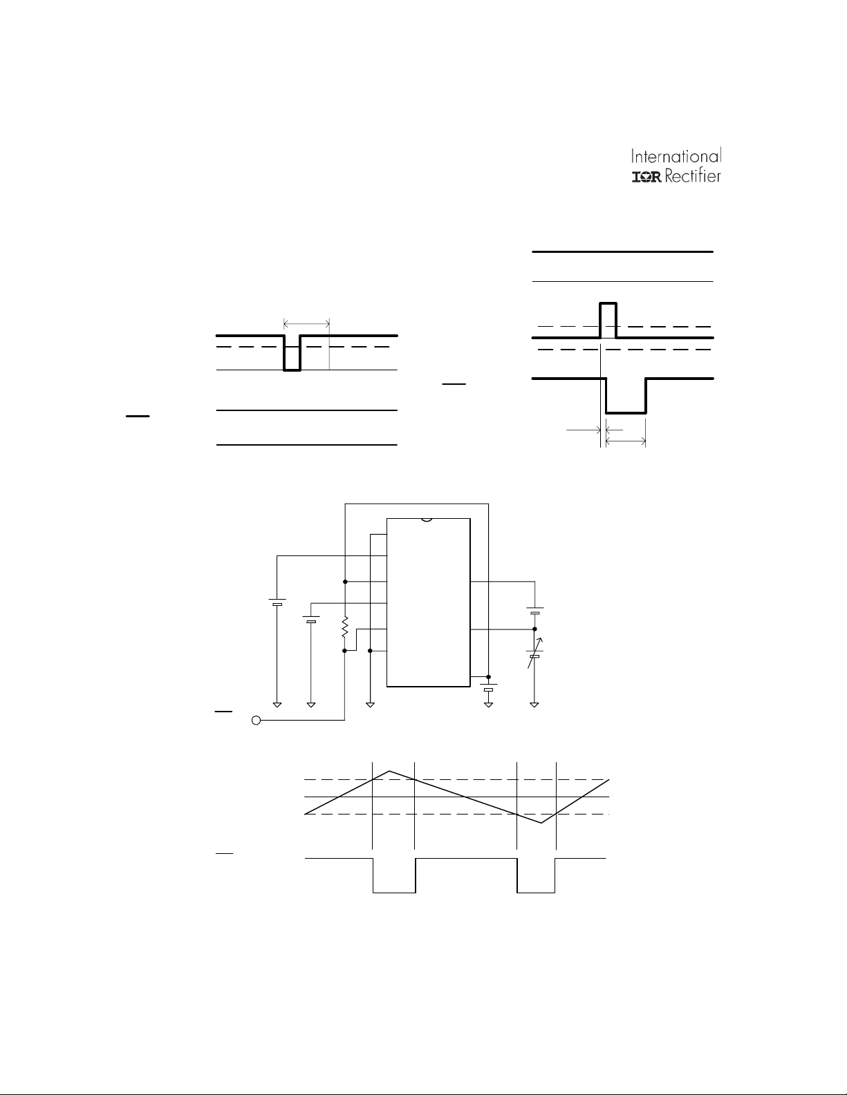
toc filt
VS
V
soct
COM
HIGH
OC
COM
Figure 3. OC Input FilterTime Definitions
10k
IN
OCSET1
DT/SD
OCSET2
__
OC
COM
LO
VS
OC
NC
NC
VB
HO
VS
NC
CC
V
Soc+
V
COM
V
Soc-
tdoc
twoc
Figure 4. OC Waveform Definitions
15V
Vsoc+
Vsoc-
15V
OC
Vsoc+
VS
COM
Vsoc-
OC
Figure 5. OC Waveform Definitions
8 www.irf.com
Page 9

IRS20124S(PbF)
p
200
160
120
80
40
Turn-on Delay Time (ns)
0
-50 -25 0 25 50 75 100 125
Temperature (
Figure 6A. Turn-On Time
vs . Tem
o
C)
erature
150
120
Max .
90
200
160
120
80
40
Turn-on Delay Time (ns)
0
10 12 14 16 18 20
V
Supply Voltage (V)
BIAS
Figure 6B. Turn-On Time
vs. Supp ly V oltage
150
120
Ma x .
90
60
Typ.
Turn-Off Time (ns)
30
0
-50-250 255075100125
o
Temperature (
C)
Figure 7A. Turn-Off Time
vs. Temperatur e
60
Ty p.
Turn-Off Time (ns)
30
0
10 12 14 16 18 20
V
Supply Voltage (V)
BIAS
Figure 7B. Turn-Off Time
vs. Supply V oltage
www.irf.com 9
Page 10

IRS20124S(PbF)
60
50
40
30
20
Turn-On Rise Time (ns)
10
-50 -25 0 25 50 75 100 125
Temperatur e (
o
C)
Fiure 8A. Turn-On Rise Time
vs.Tem perature
50
40
60
50
40
30
20
Turn-On Rise Time (ns)
10
10 12 14 16 18 20
V
Supply Voltage (V)
BIAS
Figure 8B. Turn-On Rise Time
vs. Supp ly V oltage
50
40
30
20
10
Turn-Off Fall Time (ns)
0
-50 -25 0 25 50 75 100 125
o
Temperatur e (
C)
Figure 9A. Turn-Off Fall Time
vs. Te m perat ure
30
20
10
Turn-Off Fall Time (ns)
0
10 12 14 16 18 20
Supply Voltage (V)
V
BIAS
Figure 9B. Turn-Off Fall Time
vs. Supp ly V oltage
10 www.irf.com
Page 11

IRS20124S(PbF)
pply
5
4
3
Min .
2
Input Voltage (V)
1
-50-25 0 255075100125
o
Temperature (
C)
Figure 10A. Logic "1" Input Voltage
vs. Tem perature
4
3
5
4
3
2
Input Voltage (V)
Mi n .
1
10 12 14 16 18 20
VCC Supply Voltage (V )
Figure 10B. Logic "1" Input Voltage
vs. Supply Voltage
4
3
2
Max .
Input Voltage (V)
1
0
-50-250 255075100125
Temperatre (
o
C)
Figure 11A. Logic "0" Input Voltage
vs. Temperatur e
2
Max.
Input Voltage (V)
1
0
10 12 14 16 18 20
VCC Supply Voltage (V)
Figure 11B. Logic "0" Input Voltage
vs. Su
Voltage
www.irf.com 11
Page 12

IRS20124S(PbF)
)
4
3
Max .
2
1
0
High Level Output Voltage (V)
-1
-50-250 255075100125
Temperature (
o
C)
Figure 12A. High Level Output
vs. Temperatur e
0.25
0.20
4
3
2
Ma x.
1
High Level Output Voltage (V
0
10 12 14 16 18 20
Supply Voltage (V)
V
CC
Figure 12B. High Level Output
vs. Supply Voltage
0.25
0.20
0.15
Max .
0.10
0.05
Low Level Output Voltage (V)
0.00
-50-250 255075100125
Temperature (
o
C)
Figure 13A. Low Le ve l Output
vs.Temperature
0.15
Max .
0.10
0.05
Low Level Output Voltage (V)
0.00
10 12 14 16 18 20
V
Supply Voltage (V )
CC
Figure 13B. Low Level Output
vs. Supply Voltage
12 www.irf.com
Page 13

IRS20124S(PbF)
p
300
A)
µ
250
200
150
100
Max .
50
0
-50 -25 0 25 50 75 100 125
Offset Supply Leakage Current (
Temperature (
o
C)
Figure 14A. Offset Supply Leak age
Current vs. Temperature V
=200v
B
2.5
2.0
110
A)
µ
90
70
Ma x.
50
30
Typ.
10
-10
50 80 110 140 170 200
Offset Supply Leakage Curr ent (
Boost Voltage (V)
V
B
Figure 14B. Offs e t Supply Leak age
Current vs . Supply V oltage
3
2
1.5
1.0
Supply Current ( )
0.5
BS
V
0.0
-50 -25 0 25 50 75 100 125
o
Temperatur e (
C)
Figure 15A. VBS Supply Current
vs . Te m
erature
2
1
Supply Current ( )
1
BS
V
0
10 12 14 16 18 20
V
Supply Voltage (V)
BS
Figure 15B. VBS Supply Current
vs. Supp ly V oltage
www.irf.com 13
Page 14

IRS20124S(PbF)
10
A)
µ
8
6
Max .
4
Supply Current (
2
cc
V
0
-50 -25 0 25 50 75 100 125
Temperature (
o
C)
Figur e 1 6A . VCC Supply Current
vs. Temperatur e
30
24
18
10
)
8
µΑ
6
Ma x .
4
Supply Current (
2
cc
V
0
10 12 14 16 18 20
V
Supply Voltage (V)
CC
Figu r e 16B. VCC Supply Cur r ent
vs. Supply V oltage
30
24
18
12
6
Logic "1" Input Current ( )
0
-50 -25 0 25 50 75 100 125
Temperatur e (
Figure 17A. Logic "1" Input Current
vs. Te m perat ure
o
C)
12
6
Logic "1" Input Current ( )
0
10 12 14 16 18 20
Supply V oltage ( V)
V
CC
Figure 17B. Logic "1" Input Current
vs. Supply Voltage
14 www.irf.com
Page 15

IRS20124S(PbF)
5
)
µΑ
4
3
2
Max .
1
Logic "0" Input Current (
0
-50-250 255075100125
Temperature (
o
C)
Figure 18A. Logic "0" Input Cur rent
vs. Temperatur e
11
)
10
µΑ
Max .
9
Typ.
8
Min .
Supply Current (
7
cc
V
6
-50-25 0 255075100125
Temperature (
o
C)
5
)
µΑ
4
3
2
Max .
1
Logic "0" Input Current (
0
10 12 14 16 18 20
V
Supply Voltage (V)
CC
Figure 18B. Logic "0" Input Current
vs. Supply Voltage
11
)
10
µΑ
Ma x .
9
Ty p.
8
Supply Current (
Mi n .
cc
7
V
6
-50-250 255075100125
Temperature (
o
C)
Figur e 1 9. V
Undervoltage Thres hold (+)
CC
vs. Temperatur e
Figure 20. VCC Undervoltage Thres hold (-)
vs. Te m per atur e
www.irf.com 15
Page 16

IRS20124S(PbF)
11
10
9
8
Supply Current ( )
BS
7
V
6
-50 -25 0 25 50 75 100 125
o
Temperature (
C)
Figure 21. VBS Undervoltage Thres hold (+)
vs. Tem per ature
1.5
)
Α
1.3
11
10
9
8
Supply Current ( )
BS
7
V
6
-50-25 0 25 50 75100125
Temperature (
o
C)
Figure 22. VBS Undervoltage Thres hold (-)
vs. Tem per ature
1.5
)
Α
1.3
1.1
0.9
Typ.
0.7
Output Source Current (
0.5
10 12 14 16 18 20
V
Supply Voltage (V)
BIAS
Figure 23. Output Sour ce Current
vs. Supply Voltage
1.1
0.9
Ty p.
0.7
Output Sink Current (
0.5
10 12 14 16 18 20
V
Supply V oltage (V)
BIAS
Figure 24. Output Sink Current
vs. Supply V oltage
16 www.irf.com
Page 17

IRS20124S(PbF)
-5
Typ.
-7
-9
-11
-13
VS Offset Supply Voltage (V)
-15
10 12 14 16 18 20
V
Floting Supply Voltage (V)
BS
Figure 25. Maximum VS Negative Offs et
vs. Supply Voltage
11
10
Max .
9
Typ.
8
VDT 2(V)
Min .
7
16
Max .
15
14
Typ.
13
VDT 1(V)
Min .
12
11
-50 -25 0 25 50 75 100 125
Temperature (
o
C)
Figure 26. DT mode select Threshold (1)
vs. Temperatur e
8
7
Max .
6
Ty p.
5
VDT 3(V)
Min .
4
6
-50 -25 0 25 50 75 100 125
Temperature (
o
C)
Figure 27. DT mode select Threshold (2)
vs. Temperatur e
3
-50 -25 0 25 50 75 100 125
Temperature (
o
C)
Figure 28. DT mode select Threshold (3)
vs. Temperatur e
www.irf.com 17
Page 18

IRS20124S(PbF)
)
p
p
4.5
4.0
3.5
3.0
VDT 4(V)
2.5
2.0
-50 -25 0 25 50 75 100 125
Temperatur e (
o
C)
Figure 29. DT mode se lect Thres hold (4)
vs. Te m perat ure
2.0
1.6
Ma x.
1.2
Typ .
0.8
Min .
0.4
Positive OC TH(V)
60
52
44
(nsec)
36
LO-HO
DT
Typ .
28
20
-50 -25 0 25 50 75 100 125
Temperature (
o
C)
Figure 30. DT LO turn-off to HO turn-on (3)
vs . Tem pe r atur e
-0.3
Ma x .
-0.6
-0.9
Ty p.
-1.2
Min .
Negativ e OC TH(V
-1.5
0.0
-50 -25 0 25 50 75 100 125
Temperature (
o
C)
Figure 31. Positive OC Threshold(+) in VS
vs . Tem
erature
-1.8
-50-25 0 255075100125
Temperature (
o
C)
Figure 32. Negative OC Thr es hold(-) in V S
vs. Te m
erature
18 www.irf.com
Page 19

IRS20124S(PbF)
65
55
C)
o
45
35
Temperature (
25
15
1 10 100 1000
Frequency (KHZ)
Figure 32. IRS20124s vs . Freque ncy (IRFBC20)
33.
R
=33Ω, VCC=12V
gate
65
55
C)
o
45
35
Temperature (
25
14 0 V
70V
0V
14 0 V
70V
65
55
C)
o
45
14 0 v
70v
0v
35
Temperature (
25
15
1 10 100 1000
Frequency (KHZ)
Figure 33. IRS20124s vs. Fre q ue ncy (I RFBC30)
34.
R
=22Ω, VCC=12V
gate
75
65
C)
o
0V
55
14 0 V
70V
0V
45
35
Temperature (
25
15
1 10 100 1000
Frequency (KHZ)
35.
Figure 34. IRS20124s vs . Freque ncy (IRFBC40)
R
=15Ω, VCC=12V
gate
15
1 10 100 1000
Frequency (KHZ)
36.
Figure 35. IRS20124s vs . Freque ncy (IRFPE50)
R
=10Ω, VCC=12V
gate
www.irf.com 19
Page 20

IRS20124S(PbF)
Functional description
Programmable Dead-time
The IRS20124 has an internal dead-time generation
block to reduce the number of external components
in the output stage of a Class D audio amplifier.
Selectable dead-time through the DT/SD pin voltage is an easy and reliable function, which requires only two external resistors. The dead-time
generation block is also designed to provide a
constant dead-time interval, independent of Vcc
fluctuations. Since the timings are critical to the
audio performance of a Class D audio amplifier,
the unique internal dead-time generation block is
designed to be immune to noise on the DT/SD
pin and the Vcc pin. Noise-free programmable
dead-time function is available by selecting deadtime from four preset values, which are optimized
and compensated.
How to Determine Optimal Dead-time
Please note that the effective dead-time in an actual
application differs from the dead-time specified in
this datasheet due to finite fall time, tf. The deadtime value in this datasheet is defined as the time
period from the starting point of turn-off on one
side of the switching stage to the starting point of
turn-on on the other side as shown in Fig.5. The
fall time of MOSFET gate voltage must be subtracted from the dead-time value in the datasheet
to determine the effective dead time of a Class D
audio amplifier.
(Effective dead-time)
= (Dead-time in datasheet) – (fall time, tf)
90%
HO (or LO)
10%
LO (or HO)
Figure 6. Effective Dead-time
A longer dead time period is required for a MOSFET
with a larger gate charge value because of the
longer tf. A shorter effective dead-time setting is
always beneficial to achieve better linearity in the
Class D switching stage. However, the likelihood
of shoot-through current increases with narrower
dead-time settings in mass production. Negative
values of effective dead-time may cause excessive
heat dissipation in the MOSFETs, potentially
leading to their serious damage. To calculate the
optimal dead-time in a given application, the fall
time tf for both output voltages, HO and LO, in the
actual circuit needs to be measured. In addition,
the effective dead-time can also vary with
temperature and device parameter variations.
Therefore, a minimum effective dead-time of 10nS
is recommended to avoid shoot-through current
over the range of operating temperatures and
supply voltages.
Effective dead-time
tf
Dead-
10%
20 www.irf.com
Page 21

IRS20124S(PbF)
DT/SD pin
DT/SD pin provides two functions: 1) setting deadtime and 2) shutdown. The IRS20124 determines
its operation mode based on the voltage applied
to the DT/SD pin. An internal comparator
translates which mode is being used by comparing
internal reference voltages. Threshold voltages for
each mode are set internally by a resistive voltage
divider off Vcc, negating the need of using a precise
absolute voltage to set the mode.
The relationship between the operation mode and
the voltage at DT/SD pin is illustrated in the Fig.7.
Operational Mode
15nS
25nS
Dead-time
35nS
45nS
Shutdown
Figure 7. Dead-time Settings vs VDT Voltage
V
Vcc 0.89xVcc 0.57xVcc 0.36xVcc 0.23xVcc
Design Example
Table 1 shows suggested values of resistance for
setting the deadtime. Resistors with
up to 5% tolerance
can be used if these
listed values are followed.
>0.5mA
R1
R2
Figure 8. External Resistor
IRS20124
Vcc
DT/SD
COM
Dead-
R1 R2 DT/ SD
time
mode
DT1 <10k Open 1.0 x Vcc
DT2 3.3k 8.2k 0.71 x Vcc
DT3 5.6k 4.7k 0.46 x Vcc
DT4 8.2k 3.3k 0.29 x Vcc
Table 1. Suggested resistor values for dead-time
settings
Shutdown
Since IRS20124 has internal dead-time generation, independent inputs for HO and LO are no
longer provided. Shutdown mode is the only way
to turn off both MOSFETs simultaneously to protect them from over current conditions. If the DT/
SD pin detects an input voltage below the threshold, V
the IRS20124 will output 0V at both HO
DT4,
and LO outputs, forcing the switching output node
to go into a high impedance state.
Over Current Sensing
DT
In order to protect the power MOSFET, IRS20124
has a feature to detect over current conditions,
which can occur when speaker wires are shorted
together. The over current shutdown feature can
be configured by combining the current sensing
function with the shutdown mode via the DT/SD pin.
Load Current Direction in Class D Audio
Application
In a Class D audio amplifier, the direction of the
load current alternates according to the audio input signal. An over current condition can therefore
happen during either a positive current cycle or a
negative current cycle. Fig.9 shows the rela-
voltage
www.irf.com 21
Page 22

IRS20124S(PbF)
tionship between output current direction and
the current in the low side MOSFET. It should be
noted that each MOSFET carries a part of the
load current in an audio cycle. Bi-directional current sensing offers over current detection capabilities in both cases by monitoring only the low
side MOSFET.
Load Current
0
Figure 9. Direction in MMOSFET Current and Load
Current
Bi-directional Current Sensing
IRS20124 has an over current detection function
utilizing R
of the low side switch as a current
DS(ON)
sensing shunt resistor. Due to the proprietary HVIC
process, the IRS20124 is able to sense negative
as well as positive current flow, enabling bi-directional load current sensing without the need for
any additional external passive components.
v
s
~~~
Vsoc+
~~~
~
~
~~~~~~~
~
~
~
~~~
~
IRS20124 measures the current during the period
when the low side MOSFET is turned on. Fig.10
illustrates how an excessive voltage at Vs node
detects an over current condition. Under normal
operating conditions, Vs voltage for the low side
switch is well within the trip threshold boundaries,
V
SOC-
and V
In the case of Fig.9(b) which dem-
SOC+.
onstrates the amplifier sourcing too much current
to the load, the Vs node is found below the trip
level, V
. In Fig.9(c) with opposite current direc-
SOC-
tion, the amplifier sinks too much current from the
load, positioning Vs well above trip level, V
SOC+.
Once the voltage in Vs exceeds the preset threshold, the OC pin pulls down to COM to detect an
over current condition.
Since the switching waveform usually contains
over/under shoot and associated oscillatory artifacts on their transient edges, a 200ns blanking
interval is inserted in the Vs voltage sensing block
at the instant the low side switch is engaged.
Because of this blanking interval, the OC function
will be unable to detect over current conditions if
the low side ON duration less than 200ns.
OR
LO
OC
AND
Vs
+
-
OC
SET1
OC
SET2
+
-
Figure 11. Simplified Functional Block Diagram of
Bi-Directional Current Sensing
COM
Vsoc-
(a ) Normal Operati on
Condition
(b) Over- Current in
Positive Load Current
(c ) Over- Current in
Negative Load Current
Figure 10. Vs Waveform in Over-current Condition
As shown in Fig.11, bi-directional current sensing block has an internal 2.0V level shifter feeding
the signal to the comparator. OC
tive side threshold, and is given a trip level at V
which is OC
OC
, V
SET2
- 2.0V. In same way, for a given
SET1
is set at OC
SOC-
SET2
sets the posi-
SET1
– 2.0V
SOC+
22 www.irf.com
,
Page 23

IRS20124S(PbF)
>0.5mA
Vcc
R3
OC
SET1
R4
OC
SET2
R5
COM
Figure 12. External Resistor Network to set OC
Threshold
How to set OC Threshold
The positive and negative trip thresholds for bidirectional current sensing are set by the voltages
at OC
and OC
SET1
. Fig.14 shows a typical re-
SET2
sistor voltage divider that can. be used to set
OC
and OC
SET1
The trip threshold voltages, V
determined by the required trip current levels, I
and I
TRIP-
, and R
.
SET2
SOC+
in the low side MOSFET.
DS(ON)
and V
SOC+,
are
TRIP+
Since the sensed voltage of Vs is shifted up by
2.21V internally and compared with the voltages
fed to the OC
value of OC
V
OCSET1
= V
The same relation holds between OC
V
OCSET2
= V
In general, R
and OC
SET1
with respect to COM is
SET1
+ 2.21 = I
SOC+
+ 2.21 = I
SOC-
has a positive temperature co-
DS(ON)
SET2
TRIP+
TRIP-
pins, the required
x R
x R
DS(ON)
SET2
DS(ON)
+ 2.21
and V
+ 2.21
SOC-,
efficient that needs to be considered when the
threshold level is being set. Please also note that,
in the negative load current direction, the sensing
voltage at the Vs node is limited by the body diode of the low side MOSFET as explained later.
Design Example
This example demonstrates how to use the external? resistor network to set I
be ±11A, using a MOSFET that has R
TRIP+
and I
TRIP-
to
DS(ON)
=60mÙ.
V
= VTH+ + 2.21 = I
ISET1
TRIP+
x R
+ 2.21= 11
DS(ON)
x 60mÙ +2.21 = 2.87V
V
= V
ISET2
+ 2.21 = I
TH-
TRIP-
x R
+ 2.21= (-11)
DS(ON)
x 60mÙ +2.21 = 1.55V
The total resistance of resistor network is based
on the voltage at the Vcc and required bias current in this resistor network.
R
=R3 + R4 + R5 = Vcc / I
total
bias
= 12V / 1mA = 12KÙ
The expected voltage across R3 is Vcc- V
ISET1
= 12-2.87=9.13V. Similarly, the voltages across
R4 is V
voltage across R5 is V
R3 =9.13V/ I
R4 =1.32V/ I
R5 =1.55V/ I
SOC+
- V
bias
bias
bias
= 2.87-1.55=1.32V, and the
SOC-
= 1.55V respectively.
ISET2
= 9.13KÙ
= 1.32KÙ
= 1.55KÙ
Choose R3= 9.09KÙ, R4=1.33KÙ, R5=1.54KÙ
from E-96 series.
Consequently, actual threshold levels are
V
=2.88V gives I
SOC+
V
=1.55V gives I
SOC-
TRIP+
TRIP-
= 11.2A
= -11.0A
Resisters with 1% tolerances are recommended.
www.irf.com 23
Page 24

IRS20124S(PbF)
OC Output Signal
The OC pin is a 20V open drain output. The OC
pin is pulled down to ground when an over current
condition is detected. A single external pull-up
resistor can be shared by multiple IRS20124 OC
pins to form the ORing logic. In order for a microprocessor to read the OC signal, this information
is buffered with a mono stable multi vibrator to
ensure 100ns minimum pulse width.
Because of unpredictable logic status of the OC
pin, the OC signal should be ignored during power
up/down.
Limitation from Body Diode in MOSFET
When a Class D stage outputs a positive current,
flowing from the Class D amp to the load, the body
diode of the MOSFET will turn on when the Drain
to Source voltage of the MOSFET become larger
than the diode forward drop voltage. In such a
case, the sensing voltage at the Vs pin of the
IRS20124 is clamped by the body diode. This
means that the effective Rds(on) is now much
lower than expected from Rds(on) of the MOSFET,
and the Vs node my not able to reach the threshold to turn the OC output on before the MOSFET
fails. Therefore, the region where body diode
clamping takes a place should be avoided when
setting V
SOC-
.
Voltage in Vs
0
Load
Current
}
Body Diode Clamp
Figure 13. Body Diode in MOSFET Clamps vs
Voltage
For further application information for gate driver
IC please refer to AN-978 and DT98-2a. For further application information for class D application, please refer to AN-1070 and AN-1071.
Vsoc- should be
set in this region
WORLD HEADQUARTERS: 233 Kansas St., El Segundo, California 90245 Tel: (310) 322 3331
24 www.irf.com
Data and specifications subject to change without notice. 9/21/2005
 Loading...