

Datasheet IRLU120N, IRLR120N, IRLR120NTRR, IRLR120NTRL, IRLR120NTR Datasheet (International Rectifier)
IRLR/U120N
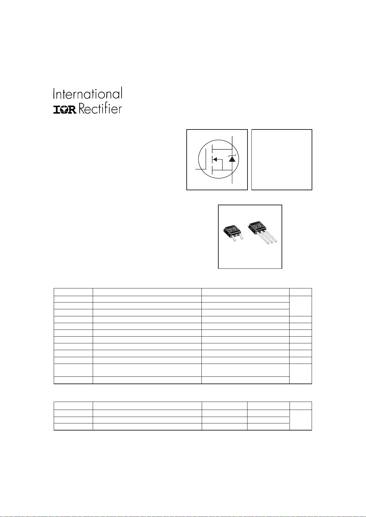
HEXFET® Power MOSFET
S
D
G
V
DSS
= 100V
R
DS(on)
= 0.185Ω
ID = 10A
Description
5/11/98
Parameter Max. Units
ID @ TC = 25°C Continuous Drain Current, VGS @ 10V 10
ID @ TC = 100°C Continuous Drain Current, VGS @ 10V 7.0 A
I
DM
Pulsed Drain Current 35
PD @TC = 25°C Power Dissipation 48 W
Linear Derating Factor 0.32 W/°C
V
GS
Gate-to-Source Voltage ± 16 V
E
AS
Single Pulse Avalanche Energy 85 mJ
I
AR
Avalanche Current 6.0 A
E
AR
Repetitive Avalanche Energy 4.8 mJ
dv/dt Peak Diode Recovery dv/dt 5.0 V/ns
T
J
Operating Junction and -55 to + 175
T
STG
Storage Temperature Range
Soldering Temperature, for 10 seconds 300 (1.6mm from case )
°C
Absolute Maximum Ratings
Parameter Typ. Max. Units
R
θJC
Junction-to-Case ––– 3.1
R
θJA
Junction-to-Ambient (PCB mount) ** ––– 50 °C/W
R
θJA
Junction-to-Ambient ––– 110
Thermal Resistance
D - P AK
TO-252AA
I-PAK
TO-251AA
l Surface Mount (IRLR120N)
l Straight Lead (IRLU120N)
l Advanced Process Technology
l Fast Switching
l Fully Avalanche Rated
Fifth Generation HEXFETs from International Rectifier
utilize advanced processing techniques to achieve the
lowest possible on-resistance per silicon area. This
benefit, combined with the fast switching speed and
ruggedized device design that HEXFET Power
MOSFETs are well known for, provides the designer
with an extremely efficient device for use in a wide
variety of applications.
The D-PAK is designed for surface mounting using
vapor phase, infrared, or wave soldering techniques.
The straight lead version (IRFU series) is for throughhole mounting applications. Power dissipation levels
up to 1.5 watts are possible in typical surface mount
applications.
PD - 91541B
www.irf.com 1
IRLR/U120N
2 www.irf.com
Parameter Min. Typ. Max. Units Conditions
V
(BR)DSS
Drain-to-Source Breakdown Voltage 100 ––– ––– V VGS = 0V, ID = 250µA
∆V
(BR)DSS
/∆T
J
Breakdown Voltage Temp. Coefficient ––– 0.12 ––– V/°C Reference to 25°C, ID = 1mA
––– ––– 0.185 VGS = 10V, ID = 6.0A
––– ––– 0.225 W VGS = 5.0V, ID = 6.0A
––– ––– 0.265 VGS = 4.0V, ID = 5.0A
V
GS(th)
Gate Threshold Voltage 1.0 ––– 2.0 V VDS = VGS, ID = 250µA
g
fs
Forward Transconductance 3.1 ––– ––– S VDS = 25V, ID = 6.0A
––– ––– 25
µA
VDS = 100V, VGS = 0V
––– ––– 250 VDS = 80V, VGS = 0V, TJ = 150°C
Gate-to-Source Forward Leakage ––– ––– 100
nA
VGS = 16V
Gate-to-Source Reverse Leakage ––– ––– -100 VGS = -16V
Q
g
Total Gate Charge ––– ––– 20 ID = 6.0A
Q
gs
Gate-to-Source Charge ––– ––– 4.6 nC VDS = 80V
Q
gd
Gate-to-Drain ("Miller") Charge ––– ––– 10 VGS = 5.0V, See Fig. 6 and 13
t
d(on)
Turn-On Delay Time ––– 4.0 ––– VDD = 50V
t
r
Rise Time ––– 35 –––
ns
ID = 6.0A
t
d(off)
Turn-Off Delay Time ––– 23 ––– RG = 11Ω, VGS = 5.0V
t
f
Fall Time ––– 22 ––– RD = 8.2Ω, See Fig. 10
Between lead,
6mm (0.25in.)
from package
and center of die contact
C
iss
Input Capacitance ––– 440 ––– VGS = 0V
C
oss
Output Capacitance ––– 97 ––– pF VDS = 25V
C
rss
Reverse Transfer Capacitance ––– 50 ––– ƒ = 1.0MHz, See Fig. 5
Electrical Characteristics @ TJ = 25°C (unless otherwise specified)
nH
I
GSS
S
D
G
L
S
Internal Source Inductance ––– 7.5 –––
R
DS(on)
Static Drain-to-Source On-Resistance
L
D
Internal Drain Inductance ––– 4.5 –––
I
DSS
Drain-to-Source Leakage Current
S
D
G
Parameter Min. Typ. Max. Units Conditions
I
S
Continuous Source Current MOSFET symbol
(Body Diode)
––– –––
showing the
I
SM
Pulsed Source Current integral reverse
(Body Diode)
––– –––
p-n junction diode.
V
SD
Diode Forward Voltage ––– ––– 1.3 V TJ = 25°C, IS = 6.0A, VGS = 0V
t
rr
Reverse Recovery Time ––– 110 160 ns TJ = 25°C, IF =6.0A
Q
rr
Reverse RecoveryCharge ––– 410 620 nC di/dt = 100A/µs
t
on
Forward Turn-On Time Intrinsic turn-on time is negligible (turn-on is dominated by LS+LD)
Source-Drain Ratings and Characteristics
A
10
35
Notes:
V
DD
= 25V, starting TJ = 25°C, L = 4.7mH
RG = 25Ω, I
AS
= 6.0A. (See Figure 12)
Repetitive rating; pulse width limited by
max. junction temperature. ( See fig. 11 )
** When mounted on 1" square PCB (FR-4 or G-10 Material ) .
For recommended footprint and soldering techniques refer to application note #AN-994
I
SD
≤ 6.0A, di/dt ≤ 340A/µs, V
DD
≤ V
(BR)DSS
,
TJ ≤ 175°C
Uses IRL520N data and test conditions.
This is applied for I-PAK, L
S
of D-PAK is measured between lead and
center of die contact
Pulse width ≤ 300µs; duty cycle ≤ 2%.
IRLR/U120N
www.irf.com 3
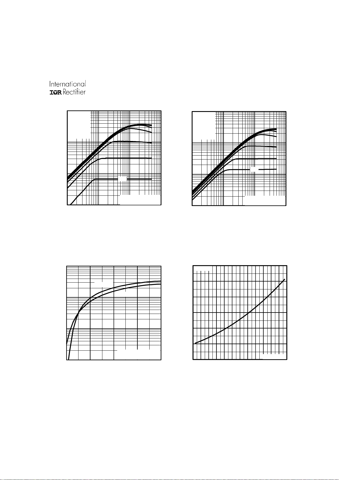
Fig 3. Typical Transfer Characteristics
Fig 4. Normalized On-Resistance
Vs. Temperature
Fig 1. Typical Output Characteristics
Fig 2. Typical Output Characteristics
and
0.1
1
10
100
0.1 1 10 100
I , D ra in-to -S o u rc e C u rre nt ( A )
D
V , D rain-to-Source V oltage (V)
DS
A
20µs PU LS E WIDTH
T = 25°C
J
VGS
TOP 15V
12V
10V
8.0V
6.0V
4.0V
3.0V
BOTTOM 2.5V
2.5V
0.1
1
10
100
0.1 1 10 100
I , D ra in-to -S o u rc e C u rre nt ( A )
D
V , D rain-to-Source V oltage (V)
DS
A
20µs PU LS E WIDTH
T = 175°C
VGS
TOP 15V
12V
10V
8.0V
6.0V
4.0V
3.0V
BOTTOM 2.5V
2.5V
J
0.1
1
10
100
246810
T = 25°C
J
GS
V , Ga te -to-S o u rc e Vo ltage (V
)
D
I , Drain-to-Source Current (A)
T = 175°C
J
A
V = 50V
20µs PULSE W IDTH
DS
0.0
0.5
1.0
1.5
2.0
2.5
3.0
-60 -40 -20 0 20 40 60 80 100 120 140 160 180
J
T , Junction Tem perature (°C)
R , D ra in -to -S o u rc e On Res is ta nc e
DS(on)
(N o rmaliz e d)
V = 10 V
GS
A
I = 1 0A
D
IRLR/U120N
4 www.irf.com
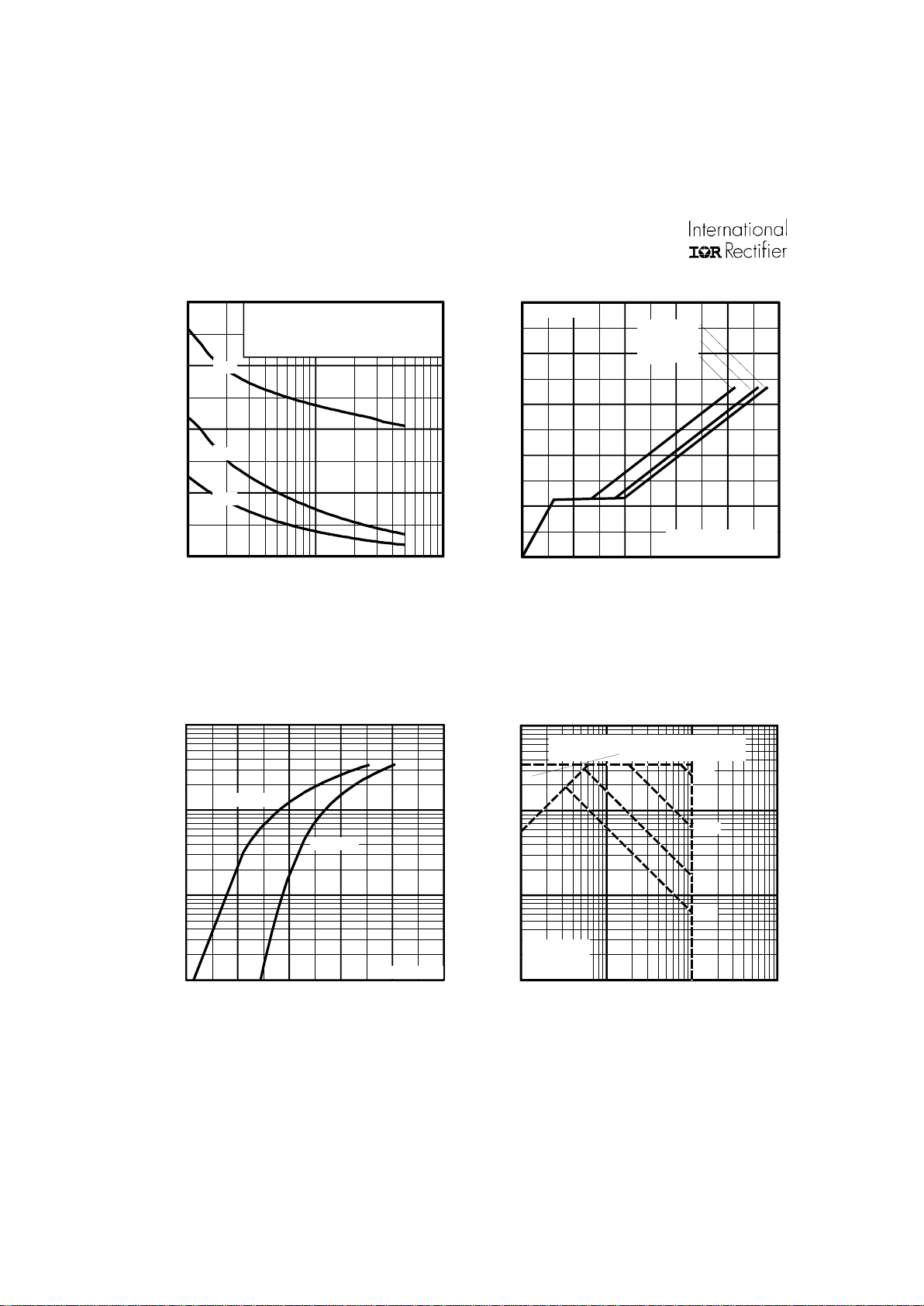
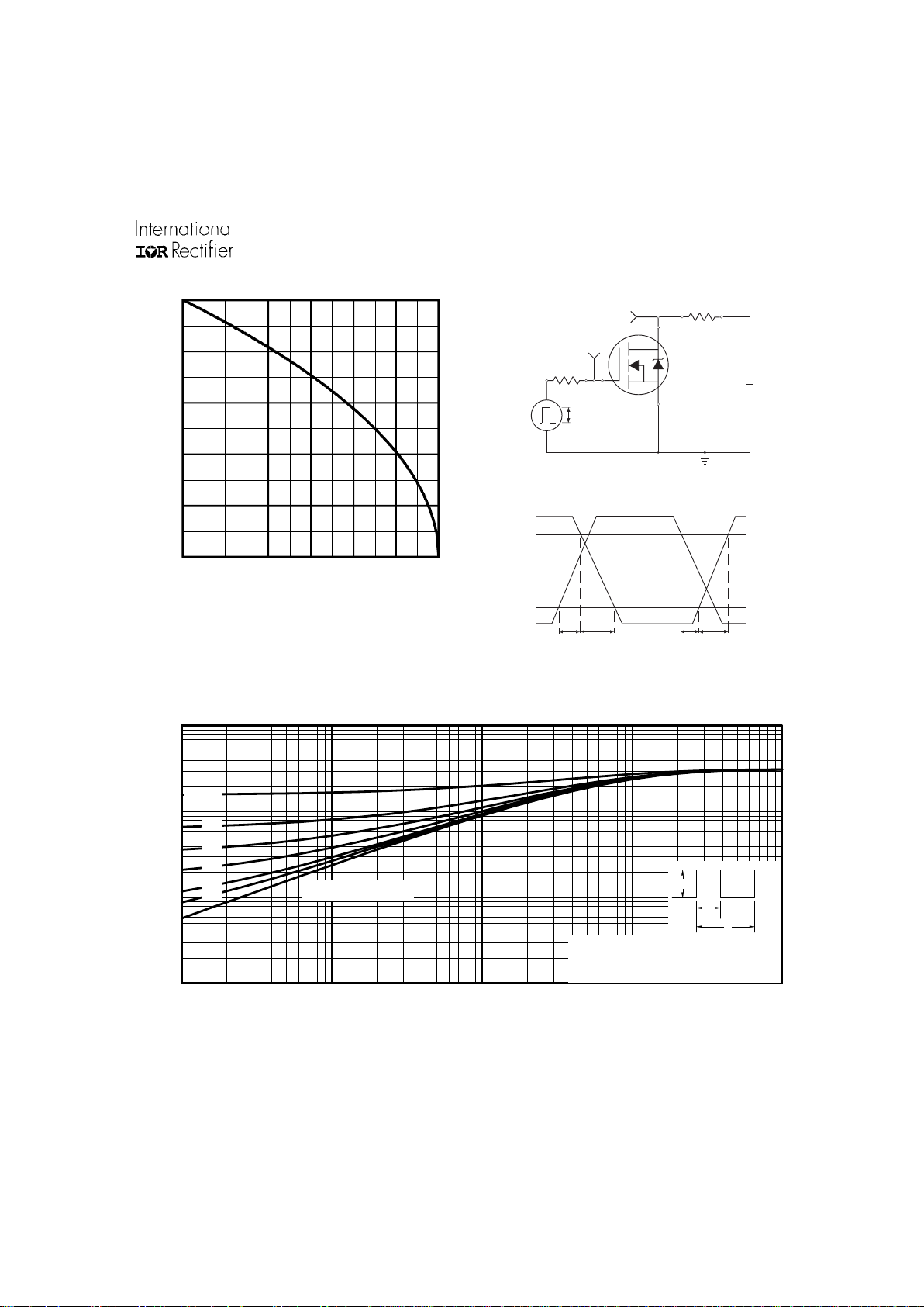
Fig 8. Maximum Safe Operating Area
Fig 6. Typical Gate Charge Vs.
Gate-to-Source Voltage
Fig 5. Typical Capacitance Vs.
Drain-to-Source Voltage
Fig 7. Typical Source-Drain Diode
Forward Voltage
0
200
400
600
800
1 10 100
C, Capacitance (pF)
DS
V , D rain-to-Source V oltage (V)
A
V = 0V, f = 1 MHz
C = C + C , C S HORTE D
C = C
C = C + C
GS
iss g s gd d s
rss g d
oss d s g d
C
iss
C
oss
C
rss
0
3
6
9
12
15
0 5 10 15 20 25
Q , T o ta l Gate Cha rg e (n C )
G
V , Ga te-to -Sou rc e V olta g e ( V )
GS
V = 80 V
V = 50 V
V = 20 V
A
FOR TEST CIRCUIT
SEE FIGURE 13
I = 6.0A
D
DS
DS
DS
0.1
1
10
100
0.4 0.6 0.8 1.0 1.2 1.4
T = 25°C
J
V = 0V
GS
V , So urce-to-Drain Voltage (V)
I , Reverse Drain Current (A)
SD
SD
A
T = 175°C
J
0.1
1
10
100
1 10 100 1000
V , D rain-to-Source V oltage (V)
DS
I , Drain Current (A)
O P E R A T IO N IN T H IS A R E A LIM IT E D
BY R
D
DS(on)
10µs
100µs
1ms
10ms
A
T = 25°C
T = 175°C
Single Pulse
C
J
IRLR/U120N
www.irf.com 5
Fig 9. Maximum Drain Current Vs.
Case Temperature
Fig 10a. Switching Time Test Circuit
V
DS
90%
10%
V
GS
t
d(on)tr
t
d(off)tf
Fig 10b. Switching Time Waveforms
V
DS
Pulse Width ≤ 1 µs
Duty Factor ≤ 0.1 %
R
D
V
GS
R
G
D.U.T.
5.0V
+
-
V
DD
Fig 11. Maximum Effective Transient Thermal Impedance, Junction-to-Case
0
2
4
6
8
10
25 50 75 100 125 150 175
C
I , Drain Current (Am ps)
D
T , Cas e Temperature (°C)
A
0.01
0.1
1
10
0.00001 0.0001 0.001 0.01 0.1
Notes:
1. Duty factor D = t / t
2. Peak T =P x Z + T
1 2
J DM thJC C
P
t
t
DM
1
2
t , Rectangular Pulse Duration (sec
)
Thermal Response (Z )
1
thJC
0.01
0.02
0.05
0.10
0.20
D = 0.50
SINGLE PULSE
(THERMAL RESPONSE)

IRLR/U120N
6 www.irf.com
Q
G
Q
GS
Q
GD
V
G
Charge
5.0 V
Fig 13b. Gate Charge Test Circuit
Fig 13a. Basic Gate Charge Waveform
Fig 12c. Maximum Avalanche Energy
Vs. Drain Current
D.U.T .
V
DS
I
D
I
G
3mA
V
GS
.3µF
50KΩ
.2µF
12V
Current Regulator
Same Type as D.U.T .
Current Sampling Resistors
+
-
Fig 12b. Unclamped Inductive Waveforms
Fig 12a. Unclamped Inductive Test Circuit
t
p
V
(BR)DSS
I
AS
R
G
I
AS
0.01
Ω
t
p
D.U.T
L
V
DS
+
-
V
DD
DRIVER
A
15V
10V
0
40
80
120
160
200
25 50 75 100 125 150 175
J
E , Single Pulse Avalanche Energy (mJ)
AS
A
Starting T , Junction Tem perature (°C)
I
TO P 2.4A
4.2A
BOTTOM 6.0A
D

IRLR/U120N
www.irf.com 7
P.W.
Period
di/dt
Diode Recovery
dv/dt
Ripple ≤ 5%
Body Diode Forward Drop
Re-Applied
Voltage
Reverse
Recovery
Current
Body Diode Forward
Current
VGS=10V
V
DD
I
SD
Driver Gate Drive
D.U.T. ISDWaveform
D.U.T. VDSWaveform
Inductor Curent
D =
P.W.
Period
+
-
+
+
+
-
-
-
Fig 14. For N-Channel HEXFETS
* V
GS
= 5V for Logic Level Devices
Peak Diode Recovery dv/dt Test Circuit
R
G
V
DD
• dv/dt controlled by R
G
• Driver same type as D.U.T.
• ISD controlled by Duty Factor "D"
• D.U.T. - Device Under Test
D.U.T
Circuit Layout Considerations
• Low Stray Inductance
• Ground Plane
• Low Leakage Inductance
Current Transformer
*

IRLR/U120N
8 www.irf.com
Package Outline
TO-252AA Outline
Dimensions are shown in millimeters (inches)
TO-252AA (D-PARK)
Part Marking Information
6.73 (.265)
6.35 (.250)
- A -
4
1 2 3
6.22 (.245)
5.97 (.235)
- B -
3X
0.89 (.035)
0.64 (.025)
0.25 (.010) M A M B
4.57 (.180)
2.28 (.090)
2X
1.14 (.045)
0.76 (.030)
1.52 (.060)
1.15 (.045)
1.02 (.040)
1.64 (.025)
5.46 (.215)
5.21 (.205)
1.27 (.050)
0.88 (.035)
2.38 (.094)
2.19 (.086)
1.14 (.045)
0.89 (.035)
0.58 (.023)
0.46 (.018)
6.45 (.245)
5.68 (.224)
0.51 (.020)
MIN .
0.58 (.023)
0.46 (.018)
LEAD ASSIGNMENTS
1 - G ATE
2 - D RAIN
3 - S OURCE
4 - D RAIN
10.42 (.410)
9.40 (.370)
NOTES:
1 DIMENSIONING & TOLERANC ING PE R AN SI Y14.5M, 1982.
2 CONTROLLING DIMENSION : INCH.
3 C ONFORMS TO J EDE C OUT LINE T O-25 2 AA.
4 DIMENSIONS SHOW N ARE BEFORE SOLDER DIP,
SOLDER D IP MAX. +0.16 (.006).
INTERNATIONAL
R EC T IF IER
L OG O
ASSEMBLY
L O T C OD E
E XAM PL E : T HIS IS A N IR F R1 2 0
W ITH A SSEM BLY
LO T CO D E 9 U 1P
FIRST PORTION
OF PART NUMBER
SECOND PORTION
OF PART NUMBER
120
IRFR
9 U 1 P
A

IRLR/U120N
www.irf.com 9
Package Outline
TO-251AA Outline
Dimensions are shown in millimeters (inches)
TO-251AA (I-PARK)
Par t Marking Information
6.73 (.265)
6.35 (.250)
- A -
6.22 (.245)
5.97 (.235)
- B -
3X
0.89 (.035)
0.64 (.025)
0.25 (.010) M A M B
2.28 (.090)
1.14 (.045)
0.76 (.030)
5.46 (.215)
5.21 (.205)
1.27 (.050)
0.88 (.035)
2.38 (.094)
2.19 (.086)
1.14 (.045)
0.89 (.035)
0.58 (.023)
0.46 (.018)
LEAD ASSIGNMENTS
1 - G ATE
2 - D RAIN
3 - S OURCE
4 - D RAIN
NOTES:
1 DIMEN S IONING & TOLERA N C ING PER AN S I Y14.5M, 1982.
2 CONTROLLING DIMENSION : INCH.
3 C ONFORMS TO J EDEC OUTLINE TO -252AA.
4 DIMENSIONS SHOW N ARE BEFORE SOLDER DIP,
SO LDE R DIP MAX. +0 .1 6 ( .0 06).
9.65 (.380)
8.89 (.350)
2X
3X
2.28 (.090)
1.91 (.075)
1.52 (.060)
1.15 (.045)
4
1 2 3
6.45 (.245)
5.68 (.224)
0.58 (.023)
0.46 (.018)
INTERNATIONAL
R E CTI F IE R
L O GO
ASSEMBLY
L O T C OD E
FIRST POR TION
OF PART NUMBE
R
SECOND PORTION
OF PART NUMBER
120
9U 1P
EXAMPLE : THIS IS AN IRFU120
WITH ASSEMBLY
L OT C O DE 9 U1 P
IR F U

IRLR/U120N
10 www.irf.com
Tape & Reel Information
TO-252AA
TR
16 . 3 ( .641 )
15 . 7 ( .619 )
8.1 ( .318 )
7.9 ( .312 )
12 .1 ( .47 6 )
11 .9 ( .46 9 )
FEED DIRECTION
FEED DIRECTION
16 .3 ( .64 1 )
15 .7 ( .61 9 )
TRR
TRL
NOTES :
1. CONTROLLING DIMENSION : MILLIMETER.
2. ALL DIMENSIONS ARE SHOWN IN MILLIM ETERS ( INCHES ).
3. OU TLINE CONFORM S TO EIA-481 & EIA-541.
NOTES :
1. OUTLINE CONFO RMS T O EIA-481.
16 mm
13 INC H
WORLD HEADQUARTERS: 233 Kansas St., El Segundo, California 90245, Tel: (310) 322 3331
EUROPEAN HEADQUARTERS: Hurst Green, Oxted, Surrey RH8 9BB, UK Tel: ++ 44 1883 732020
IR CANADA: 15 Lincoln Court, Brampton, Ontario L6T 3Z2, Tel: (905) 453 2200
IR GERMANY: Saalburgstrasse 157, 61350 Bad Homburg Tel: ++ 49 6172 96590
IR ITALY: Via Liguria 49, 10071 Borgaro, Torino Tel: ++ 39 11 451 0111
IR FAR EAST: 171 (K&H Bldg.) 30-4 Nishi-ikebukuro 3-chome, Toshima-ku, Tokyo Japan Tel: 81 33 983 0086
IR SOUTHEAST ASIA: 315 Outram Road, #10-02 Tan Boon Liat Building, Singapore 16907 Tel: 65 221 8371
Data and specifications subject to change without notice. 5/98
 Loading...