

Page 1
查询IRHNA9260供应商查询IRHNA9260供应商
RADIATION HARDENED
POWER MOSFET
SURFACE MOUNT (SMD-2)
Product Summary
Part Number Radiation Level RDS(on) ID QPL Part Number
IRHNA9260 100K Rads (Si) 0.154Ω -29A JANSR2N7426U
IRHNA93260 300K Rads (Si) 0.154Ω -29A JANSF2N7426U
JANSR2N7426U
200V , P-CHANNEL
REF: MIL-PRF-19500/655
RAD-Hard™ HEXFET
PD - 93969
IRHNA9260
®
TECHNOLOGY
International Rectifier’s RAD-HardTM HEXFET
MOSFET technology provides high performance
power MOSFETs for space applications. This technology has over a decade of proven performance
and reliability in satellite applications. These devices have been characterized for both Total Dose
and Single Event Effects (SEE). The combination
of low R
power losses in switching applications such as DC
to DC converters and motor control. These devices retain all of the well established advantages
of MOSFETs such as voltage control, fast switching, ease of paralleling and temperature stability
of electrical parameters.
DS(on) and low gate charge reduces the
Absolute Maximum Ratings
Parameter Units
ID @ VGS = -12V , TC = 25°C Continuous Drain Current -29
ID @ VGS = -12V , TC = 100°C Continuous Drain Current -18
I
DM
PD @ TC = 25°C Max. Power Dissipation 300 W
V
GS
E
AS
I
AR
E
AR
dv/dt Peak Diode Recovery dv/dt ➂ -20
T
J
T
STG
Pulsed Drain Current ➀ -116
Linear Derating Factor 2.4 W/°C
Gate-to-Source Voltage ±20 V
Single Pulse Avalanche Energy ➁ 500 mJ
Avalanche Current ➀ -29 A
Repetitive Avalanche Energy ➀ 30 mJ
Operating Junction -55 to 150
Storage Temperature Range
Pckg. Mounting Surface Temp. 300 (for 5s)
Weight 3.3 (Typical) g
®
Features:
n Single Event Effect (SEE) Hardened
n Ultra Low RDS(on)
n Lo w Total Gate Charge
n Proton Tolerant
n Simple Drive Requirements
n Ease of P aralleling
n Hermetically Sealed
n Surface Mount
n Cer amic Package
n Light W eight
Pre-Irradiation
SMD-2
A
V/ns
o
C
For footnotes refer to the last page
www.irf.com 1
11/21/00
Page 2
IRHNA9260, JANSR2N7426U Pre-Irradiation
Electrical Characteristics @ Tj = 25°C (Unless Otherwise Specified)
Parameter Min Typ Max Units T est Conditions
BV
DSS
∆BV
R
DS(on)
V
GS(th)
g
fs
I
DSS
I
GSS
I
GSS
Q
g
Q
gs
Q
gd
t
d(on)
t
r
t
d(off)
t
f
LS + L
DSS
D
Drain-to-Source Breakdown V oltage -200 — — V VGS = 0V, ID = -1.0mA
/∆TJT emperature Coefficient of Breakdown — -0.27 — V/°C Reference to 25°C, ID = -1.0mA
Voltage
Static Drain-to-Source On-State — — 0.154 Ω VGS = -12V, ID = -18A
Resistance — — 0.159 VGS = -12V, ID = -29A
Gate Threshold V oltage -2.0 — -4.0 V VDS = VGS, ID = -1.0mA
Forward T ransconductance 14 — — S ( )VDS > -15V, IDS = -18A ➃
Zero Gate V oltage Drain Current — — -25 VDS= -160V ,VGS=0V
— — -250 VDS = -160V ,
Gate-to-Source Leakage Forward — — -100 VGS = -20V
Gate-to-Source Leakage Reverse — — 100 VGS = 20V
T otal Gate Charge — — 300 VGS = -12V, ID = -29A
Gate-to-Source Charge — — 65 n C VDS = -100V
Gate-to-Drain (‘Miller’) Charge — — 58
T urn-On Delay Time — — 37 VDD = -100V, ID = -29A
Rise Time — — 141 RG = 2.35Ω
T urn-Off Delay Time — — 148
Fall Time — — 22 0
T otal Inductance — 4.0 —
Ω
µA
VGS = 0V, TJ = 125°C
nA
ns
nH
Measured from the center of
drain pad to center of source pad
➃
C
iss
C
oss
C
rss
Input Capacitance — 6143 — VGS = 0V, VDS = -25V
Output Capacitance — 915 — pF f = 1.0MHz
Reverse T ransf er Capacitance — 159 —
Source-Drain Diode Ratings and Characteristics
Parameter Min Typ Max Units Test Conditions
I
Continuous Source Current (Body Diode) — — - 29
S
I
Pulse Source Current (Body Diode) ➀ — — -116
SM
V
Diode Forward V oltage — — -3.0 V Tj = 25°C, IS = -29A, VGS = 0V ➃
SD
t
Reverse Recov ery Time — — 73 8 ns Tj = 25°C, IF = -29A, di/dt ≤ -100A/µs
rr
Q
Reverse Recovery Charge — — 12 µCV
RR
t
Forward T urn-On Time Intrinsic turn-on time is negligible. Turn-on speed is substantially controlled by L
on
A
≤ -50V ➃
DD
Thermal Resistance
Parameter Min Typ Max Units Test Conditions
R
thJC
R
thJ-PCB
Note: Corresponding Spice and Saber models are available on the G&S Website.
For footnotes refer to the last page
2 www.irf.com
Junction-to-Case — — 0.42
Junction-to-PC board — 1.6 — soldered to a 2” square copper-clad board
°C/W
+ LD.
S
Page 3
Radiation Characteristics
IRHNA9260, JANSR2N7426U
International Rectifier Radiation Hardened MOSFETs are tested to verify their radiation hardness capability .
The hardness assurance program at International Rectifier is comprised of two radiation environments.
Every manufacturing lot is tested for total ionizing dose (per notes 5 and 6) using the TO-3 package. Both
pre- and post-irradiation performance are tested and specified using the same drive circuitry and test
conditions in order to provide a direct comparison.
Table 1. Electrical Characteristics @ Tj = 25°C, Post Total Dose Irradiation ➄➅
BV
V
I
GSS
I
GSS
I
DSS
R
Parameter 100K Rads(Si)
Drain-to-Source Breakdown Voltage -200 — -200
DSS
GS(th)
DS(on)
Gate Threshold Voltage ➃ -2.0 -4.0 -2.0 -5.0 VGS = VDS, ID = -1.0mA
Gate-to-Source Leakage Forward — -100 — -100
Gate-to-Source Leakage Reverse — 100 — 10 0 VGS = 20 V
Zero Gate Voltage Drain Current — - 25 — -25 µA VDS= -160V, V
Static Drain-to-Source ➃ — 0.155 — 0.161 Ω VGS = -12V, ID =-18A
Min Max Min Max
1
300K Rads (Si)
2
Units
Test Conditions
—
VGS = 0V, ID = -1.0mA
V
nA
VGS = -20V
GS
=0V
On-State Resistance (TO-3)
R
DS(on)
Static Drain-to-Source ➃ — 0.154 — 0.160 Ω VGS = -12V, ID = -18A
On-State Resistance (SMD-2)
V
SD
1. Part number IRHNA9260
2. Part number IRHNA93260
Diode Forward Voltage ➃ — -3.0 — -3.0 V VGS = 0V, IS = -29A
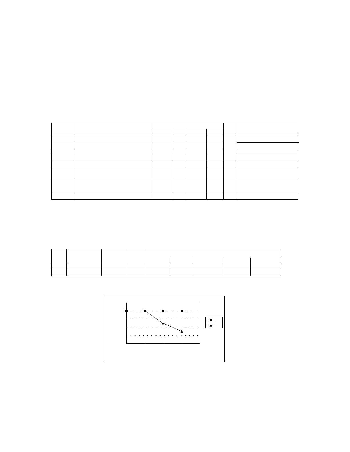
International Rectifier radiation hardened MOSFETs have been characterized in heavy ion environment for
Single Event Effects (SEE). Single Event Effects characterization is illustrated in Fig. a and Table 2.
Table 2. Single Event Effect Safe Operating Area
Io n LET Energy Range
MeV/(mg/cm2)) (MeV) (µm) @VGS=0V @VGS=5V @VGS=10V @VGS=15V @VGS=20V
Cu 28.0 285 43.0 -200 -200 -200 -200 —
Br 36.8 305 39.0 -200 -200 -125 -75 —
-250
-200
-150
VDS
-100
-50
0
0 5 10 15 20
VGS
VDS (V)
Cu
Br
Fig a. Single Event Effect, Safe Operating Area
For footnotes refer to the last page
www.irf.com 3
Page 4

IRHNA9260, JANSR2N7426U Pre-Irradiation
1000
100
D
-I , Drain-to-Source Current (A)
10
1000
VGS
TOP
-15V
-12V
-10V
-9.0V
-8.0V
-7.0V
-6.0V
BOTTOM
-5.0V
-5.0V
20µs PULSE WIDTH
1 10 100
-V , Drain-to-Source Voltage (V)
DS
°
T = 25 C
J
1000
100
D
-I , Drain-to-Source Current (A)
10
1 10 100
VGS
TOP
-15V
-12V
-10V
-9.0V
-8.0V
-7.0V
-6.0V
BOTTOM
-5.0V
-5.0V
20µs PULSE WIDTH
T = 150 C
J
-V , Drain-to-Source Voltage (V)
DS
°
Fig 2. Typical Output CharacteristicsFig 1. Typical Output Characteristics
2.5
-29A
I =
D
2.0
1.5
100
1.0
(Normalized)
D
-I , Drain-to-Source Current (A)
V = -50V
DS
10
5.0 6.0 7.0 8.0 9.0 10.0
-V , Gate-to-Source Voltage (V)
GS
20µs PULSE WIDTH
Fig 3. Typical Transfer Characteristics
0.5
DS(on)
R , Drain-to-Source On Resistance
0.0
-60 -40 -20 0 20 40 60 80 100 120 140 160
T , Junction Temperature( C)
J
Fig 4. Normalized On-Resistance
V =
-12V
GS
°
Vs. Temperature
4 www.irf.com
Page 5

Pre-Irradiation
IRHNA9260, JANSR2N7426U
10000
8000
6000
4000
C, Capacitance (pF)
2000
0
1 10 100
V
=
0V,
C
C
C
C
C
oss
C
iss
rss
f = 1MHz
+ C
+ C
C SHORTED
GS
C
=
iss gs gd , ds
C
=
rss gd
C
=
oss ds gd
-V , Drain-to-Source Voltage (V)
DS
Fig 5. Typical Capacitance Vs.
Drain-to-Source Voltage
1000
20
I =
-29A
D
16
12
8
4
GS
-V , Gate-to-Source Voltage (V)
0
0 50 100 150 200 250 300 350
Q , Total Gate Charge (nC)
G
V = 160V
DS
V = 100V
DS
V = 40V
DS
FOR TEST CIRCUIT
SEE FIGURE
Fig 6. Typical Gate Charge Vs.
Gate-to-Source Voltage
1000
13
OPERATION IN THIS AREA
LIMITED BY RDS(on)
100
10
1
SD
-I , Reverse Drain Current (A)
0.1
0.0 0.5 1.0 1.5 2.0 2.5 3.0 3.5
-V ,Source-to-Drain Voltage (V)
SD
T = 150 C
Fig 7. Typical Source-Drain Diode
°
J
100
°
T = 25 C
J
V = 0 V
GS
10
, Drain-to-Source Current (A)
D
Tc = 25°C
-I
Tj = 150°C
Single Pulse
1
1 10 100 1000
-V
, Drain-toSource Voltage (V)
DS
100µs
1ms
1
0ms
Fig 8. Maximum Safe Operating Area
Forward Voltage
www.irf.com 5
Page 6

IRHNA9260, JANSR2N7426U Pre-Irradiation
R
D.U.T.
D
-
+
V
DD
30
25
R
20
V
DS
V
GS
G
-12V
15
Pulse Width ≤ 1 µs
Duty Factor ≤ 0.1 %
10
D
-I , Drain Current (A)
5
0
25 50 75 100 125 150
T , Case Temperature ( C)
C
°
Fig 9. Maximum Drain Current Vs.
Case Temperature
1
D = 0.50
thJC
0.1
0.20
0.10
0.05
0.02
0.01
0.01
Thermal Response (Z )
0.001
0.00001 0.0001 0.001 0.01 0.1 1
SINGLE PULSE
(THERMAL RESPONSE)
t , Rectangular Pulse Duration (sec)
1
Fig 10a. Switching Time Test Circuit
V
DS
90%
10%
V
GS
t
d(on)tr
t
d(off)tf
Fig 10b. Switching Time Waveforms
P
DM
t
1
Notes:
1. Duty factor D = t / t
2. Peak T = P x Z + T
1 2
J DM thJC C
t
2
Fig 11. Maximum Effective Transient Thermal Impedance, Junction-to-Case
6 www.irf.com
Page 7

Pre-Irradiation
(BR)
IRHNA9260, JANSR2N7426U
L
D.U.T
.
I
AS
0.01
p
DRIVER
Ω
V
15V
R
-20 V
-12V
V
DS
G
t
Fig 12a. Unclamped Inductive Test Circuit
I
AS
t
p
V
DSS
DD
1200
TOP
A
900
600
300
AS
E , Single Pulse Avalanche Energy (mJ)
0
25 50 75 100 125 150
Starting T , Junction Temperature ( C)
J
BOTTOM
I
D
-13A
-18.3A
-29A
°
Fig 12c. Maximum Avalanche Energy
Vs. Drain Current
Fig 12b. Unclamped Inductive Waveforms
Current Regulator
Same Type as D.U.T.
Q
G
-12 V
Q
GS
V
G
Q
GD
Charge
Fig 13a. Basic Gate Charge Waveform
-12V
12V
V
GS
Fig 13b. Gate Charge Test Circuit
50KΩ
.2µF
.3µF
-3mA
Current Sampling Resistors
V
DS
+
D.U.T.
I
G
I
D
www.irf.com 7
Page 8

IRHNA9260, JANSR2N7426U Pre-Irradiation
Footnotes:
➀ Repetitive Rating; Pulse width limited by
maximum junction temperature.
➁ V
=-50V , starting TJ = 25°C, L = 1.2mH,
DD
Peak IL= -29A, VGS = -12V
➂ I
≤ - 29A, di/dt ≤ -377A/µs,
SD
VDD ≤ - 200V, TJ ≤ 150°C
➃ Pulse width ≤ 300 µs; Duty Cycle ≤ 2%
➄ Total Dose Irradiation with V
-12 volt VGS applied and VDS = 0 during
irradiation per MIL-STD-750, method 1019, condition A
➅ Total Dose Irradiation with V
-160 volt VDS applied and VGS = 0 during
irradiation per MlL-STD-750, method 1019, condition A
GS
DS
Bias.
Bias.
Case Outline and Dimensions — SMD-2
IR EUROPEAN REGIONAL CENTRE: 439/445 Godstone Rd, Whyteleafe, Surrey CR3 OBL, UK Tel: ++ 44 (0)20 8645 8000
IR SOUTHEAST ASIA: 1 Kim Seng Promenade, Great World City West Tower, 13-11, Singapore 237994 Tel: ++ 65 (0)838 4630
IR WORLD HEADQUARTERS: 233 Kansas St., El Segundo, California 90245, USA Tel: (310) 252-7105
IR CANADA: 15 Lincoln Court, Brampton, Ontario L6T3Z2, Tel: (905) 453 2200
IR GERMANY: Saalburgstrasse 157, 61350 Bad Homburg Tel: ++ 49 (0) 6172 96590
IR ITALY: Via Liguria 49, 10071 Borgaro, Torino Tel: ++ 39 011 451 0111
IR JAPAN: K&H Bldg., 2F, 30-4 Nishi-Ikebukuro 3-Chome, Toshima-Ku, Tokyo 171 Tel: 81 (0)3 3983 0086
IR TAIWAN:16 Fl. Suite D. 207, Sec. 2, Tun Haw South Road, Taipei, 10673 Tel: 886-(0)2 2377 9936
Data and specifications subject to change without notice. 11/00
8 www.irf.com
 Loading...