

Page 1

PD - 9.1561A
PRELIMINARY
l Generation V Technology
l Ultra Low On-Resistance
l Dual N and P Channel MOSFET
l Surface Mount
l Very Low Gate Charge and
Switching Losses
l Fully Avalanche Rated
Description
Fifth Generation HEXFETs from International Rectifier
utilize advanced processing techniques to achieve
extremely low on-resistance per silicon area. This
benefit, combined with the fast switching speed and
ruggedized device design that HEXFET Power
MOSFETs are well known for, provides the designer
with an extremely efficient and reliable device for use
in a wide variety of applications.
The SO-8 has been modified through a customized
leadframe for enhanced thermal characteristics and
multiple-die capability making it ideal in a variety of
power applications. With these improvements, multiple
devices can be used in an application with dramatically
reduced board space. The package is designed for
vapor phase, infra red, or wave soldering techniques.
IRF9952
HEXFET® Power MOSFET
N-CHANNEL MOSFET
1
S1
2
G1
3
S2
4
G2
P-CHANNEL MOSFET
T op V iew
Recommended upgrade: IRF7309 or IRF7319
Lower profile/smaller equivalent: IRF7509
8
D1
7
D1
D2
D2
V
6
5
R
N-Ch P-Ch
30V -30V
DSS
0.10Ω 0.25Ω
DS(on)
SO-8
Symbol Maximum Units
N-Channel P-Channel
Drain-Source Voltage V
Gate-Source Voltage V
Continuous Drain Current
TA = 25°C 3.5 -2.3
TA = 70°C 2.8 -1.8
Pulsed Drain Current I
Continuous Source Current (Diode Conduction) I
Maximum Power Dissipation
TA = 25°C 2.0
TA = 70°C 1.3
Single Pulse Avalanche Energy E
Avalanche Current I
Repetitive Avalanche Energy E
DS
GS
I
D
DM
S
P
D
AS
AR
AR
30
± 20
16 -10
1.7 -1.3
44 57 mJ
2.0 -1.3 A
0.25 mJ
Peak Diode Recovery dv/dt dv/dt 5.0 -5.0 V/ ns
Junction and Storage Temperature Range T
J, TSTG
-55 to + 150 °C
Thermal Resistance Ratings
Parameter Symbol Limit Units
Maximum Junction-to-Ambient R
θJA
62.5
V
A
W
°C/W
8/25/97
Page 2
IRF9952
Electrical Characteristics @ TJ = 25°C (unless otherwise specified)
V
(BR)DSS
∆V
(BR)DSS
R
DS(ON)
V
GS(th)
g
fs
I
DSS
I
GSS
Q
g
Q
gs
Q
gd
t
d(on)
t
r
t
d(off)
t
f
C
iss
C
oss
C
rss
Drain-to-Source Breakdown Voltage
/∆TJBreakdown Voltage Temp. Coefficient
Static Drain-to-Source On-Resistance
Gate Threshold Voltage
Forward Transconductance
Drain-to-Source Leakage Current
Gate-to-Source Forward Leakage N-P –– — ±100 VGS = ±20V
Total Gate Charge
Gate-to-Source Charge
Gate-to-Drain ("Miller") Charge
Turn-On Delay Time
Rise Time
Turn-Off Delay Time
Fall Time
Input Capacitance
Output Capacitance
Reverse Transfer Capacitance
Parameter Min. Typ. Max. Units Conditions
N-Ch 30 — — V
P-Ch -30 — — V
N-Ch — 0.015 — Reference to 25°C, I
P-Ch — 0.015 — Reference to 25°C, I
— 0.08 0.10 V
N-Ch
— 0.12 0.15 V
— 0.1650.250 V
P-Ch
— 0.2900.400 V
V/°C
N-Ch 1.0 — — V
P-Ch -1.0 — — V
N-Ch — 12 — V
P-Ch — 2.4 — V
N-Ch — — 2.0 V
P-Ch — — -2.0 V
N-Ch — — 25 V
µA
P-Ch — — -25 V
N-Ch — 6.9 14
P-Ch — 6.1 12
N-Ch — 1.0 2.0
P-Ch — 1.7 3.4
nC
N-Ch — 1.8 3.5
P-Ch — 1.1 2.2
N-Ch — 6.2 12
P-Ch — 9.7 19
N-Ch — 8.8 18
P-Ch — 14 28
N-Ch — 13 26
ns
P-Ch — 20 40
N-Ch — 3.0 6.0
P-Ch — 6.9 14
N-Ch — 190 —
P-Ch — 190 —
N-Ch — 120 — pF
P-Ch — 110 —
N-Ch — 61 —
P-Ch — 54 —
= 0V, ID = 250µA
GS
V
= 0V, ID = -250µA
GS
= 10V, ID = 2.2A
GS
= 4.5V, ID = 1.0A
GS
Ω
= -10V, ID = -1.0A
GS
= -4.5V, ID = -0.50A
GS
= VGS, ID = 250µA
DS
V
= VGS, ID = -250µA
DS
= 15V, ID = 3.5A
DS
S
= -15V, ID = -2.3A
DS
= 24V, VGS = 0V
DS
= -24V, VGS = 0V
DS
= 24V, VGS = 0V, TJ = 125°C
DS
= -24V, VGS = 0V, TJ = 125°C
DS
nA
N-Channel
= 1.8A, VDS = 10V, VGS = 10V
I
D
P-Channel
I
= -2.3A, VDS = -10V, VGS = -10V
D
N-Channel
V
= 10V, ID = 1.0A, RG = 6.0Ω,
DD
R
= 10Ω
D
P-Channel
V
= -10V, ID = -1.0A, RG = 6.0Ω,
DD
R
= 10Ω
D
N-Channel
VGS = 0V, VDS = 15V, ƒ = 1.0MHz
P-Channel
= 0V, VDS = -15V, ƒ = 1.0MHz
V
GS
= 1mA
D
= -1mA
D
Source-Drain Ratings and Characteristics
Parameter Min. Typ. Max. Units Conditions
I
S
I
SM
V
SD
t
rr
Q
rr
Continuous Source Current (Body Diode)
Pulsed Source Current (Body Diode)
Diode Forward Voltage
Reverse Recovery Time
Reverse Recovery Charge
Notes:
Repetitive rating; pulse width limited by
max. junction temperature. ( See fig. 23 )
N-Channel I
P-Channel I
N-Channel Starting T
P-Channel Starting TJ = 25°C, L = 67mH RG = 25Ω, I
≤ 2.0A, di/dt ≤ 100A/µs, V
SD
≤ -1.3A, di/dt ≤ 84A/µs, V
SD
= 25°C, L = 22mH RG = 25Ω, I
J
DD
DD
≤ V
≤ V
N-Ch — — 1.7
P-Ch — — -1.3
N-Ch — — 16
P-Ch — — 16
N-Ch — 0.82 1.2 T
P-Ch — -0.82 -1.2 T
N-Ch — 27 53
P-Ch — 27 54
N-Ch — 28 57
P-Ch — 31 62
, TJ ≤ 150°C
(BR)DSS
, TJ ≤ 150°C
(BR)DSS
= 2.0A. (See Figure 12)
AS
= -1.3A.
AS
A
= 25°C, IS = 1.25A, VGS = 0V
J
V
= 25°C, IS = -1.25A, VGS = 0V
J
N-Channel
ns
= 25°C, IF =1.25A, di/dt = 100A/µs
T
J
P-Channel
nC
= 25°C, IF = -1.25A, di/dt = 100A/µs
T
J
Pulse width ≤ 300µs; duty cycle ≤ 2%.
Surface mounted on FR-4 board, t ≤ 10sec.
Page 3
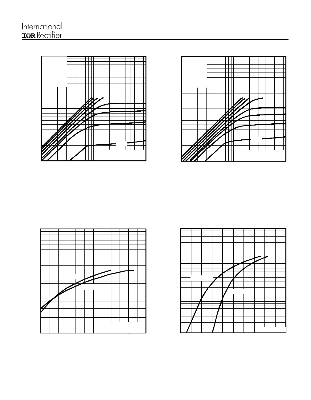
N-Channel
IRF9952
100
VGS
TOP 15V
10V
7.0V
5.5V
4.5V
4.0V
3.5V
BOTT OM 3.0V
10
D
I , Drain-to-Source Cu rrent (A)
3.0V
20µs PU LSE W IDTH
T = 25 °C
1
0.1 1 10
V , D rain-to-Source Voltage (V)
DS
J
Fig 1. Typical Output Characteristics
100
100
VGS
TOP 15V
10V
7.0V
5.5V
4.5V
4.0V
3.5V
BOTT OM 3.0V
10
D
I , Drain-to-Source Current (A)
3.0V
20µs PU LSE W IDTH
T = 150°C
A
1
0.1 1 10
V , Drain-to -Sou rce Vo ltage ( V)
DS
J
A
Fig 2. Typical Output Characteristics
100
T = 25°C
10
D
I , Dra in -to -Sou rce Curren t (A )
1
3.0 3.5 4.0 4.5 5.0 5.5 6.0
J
T = 150°C
J
V = 10V
DS
20µs PULSE W IDTH
V , Ga te-to-So urce Voltage (V)
GS
Fig 3. Typical Transfer Characteristics
10
T = 150°C
J
T = 25°C
1
SD
I , Rev ers e Dr ain C u rren t (A)
A
0.1
0.4 0.6 0.8 1.0 1.2 1.4
V , Sour c e-to-D rain Volt a ge (V)
SD
J
V = 0V
GS
A
Fig 4. Typical Source-Drain Diode
Forward Voltage
Page 4

IRF9952
N-Channel
2.0
1.5
1.0
I =
D
2.2A
(Normalized)
0.5
DS(on)
R , Drain-to-Source On Resistance
0.0
-60 -40 -20 0 20 40 60 80 100 120 140 160
T , Junction Temperature ( C)
J
Fig 5. Normalized On-Resistance
Vs. Temperature
0.16
0.14
0.12
V =
GS
°
10V
0.12
0.10
0.08
0.06
V = 4 .5V
GS
V = 10V
GS
(on) , Drain-to-Source On Resistance (Ω)
DS
R
0.04
024681012
I , Dra in C urrent (A)
D
Fig 6. Typical On-Resistance Vs. Drain
Current
100
80
I
TOP 0.89A
1.6A
BOTTOM 2.0A
D
A
0.10
0.08
0.06
0.04
0.02
(on) , Drain-to-Source On Resistance (Ω)
DS
R
0.00
0 3 6 9 12 15
V , Gate -to-Source Voltage (V)
GS
I = 3 .5 A
D
Fig 7. Typical On-Resistance Vs. Gate
Voltage
60
40
20
AS
E , Single Pulse Avalanche Energy (mJ)
A
0
25 50 75 100 125 150
Starting T , Junction Temperature (°C)
J
Fig 8. Maximum Avalanche Energy
Vs. Drain Current
A
Page 5

N-Channel
IRF9952
350
300
250
200
150
C, C apac itance (pF)
100
50
0
1 10 100
V = 0V , f = 1MHz
GS
C = C + C , C SHORTED
iss gs gd ds
C = C
rss gd
C = C + C
oss ds gd
C
iss
C
oss
C
rss
V , Drai n-to -Sourc e Volt ag e (V )
DS
Fig 9. Typical Capacitance Vs.
Drain-to-Source Voltage
100
20
I =D1.8A
16
12
8
4
GS
V , Gate-to-Source Voltage (V)
A
0
0 2 4 6 8 10
Q , Total Gate Charge (nC)
G
Fig 10. Typical Gate Charge Vs.
Gate-to-Source Voltage
V = 10V
DS
0.50
thJA
0.20
10
0.10
0.05
0.02
1
0.01
Thermal Response (Z )
0.1
0.00001 0.0001 0.001 0.01 0.1 1 10 100
SINGLE PULSE
(THERMAL RESPONSE)
Notes:
1. Duty factor D = t / t
2. Peak T = P x Z + T
t , Rectangular Pulse Duration (sec)
1
J DM thJA A
1 2
P
DM
t
1
t
2
Fig 11. Maximum Effective Transient Thermal Impedance, Junction-to-Ambient
Page 6

IRF9952
P-Channel
100
VGS
TOP - 15V
- 10V
- 7.0V
- 5.5V
- 4.5V
- 4.0V
- 3.5V
BOTT OM - 3.0V
10
1
-3.0V
D
-I , D r ain -to-S o u r c e C urre n t ( A )
20µs PU LSE W IDTH
T = 25 °C
0.1
0.1 1 10
-V , Drain-to-Source Voltage (V)
DS
J
Fig 12. Typical Output Characteristics
100
100
VGS
TOP - 15V
- 10V
- 7.0V
- 5.5V
- 4.5V
- 4.0V
- 3.5V
BOTT OM - 3.0V
10
1
-3.0V
D
-I , D r ain -to-S o u r c e C urre n t ( A )
20µs PU LSE W IDTH
T = 150°C
A
0.1
0.1 1 10
-V , Drain-to-Source Voltage (V)
DS
J
A
Fig 13. Typical Output Characteristics
100
10
T = 25°C
J
T = 150°C
J
1
D
-I , Drain -t o -S ou rce Curren t (A)
0.1
3.0 4.0 5.0 6.0 7.0 8.0
-V , G ate - to -S ource Vo l ta g e (V)
GS
V = - 1 0V
DS
20µs PULSE WIDTH
Fig 14. Typical Transfer Characteristics
10
T = 150°C
J
T = 25°C
J
1
SD
-I , Re verse D rain Current (A)
V = 0V
A
0.1
0.4 0.6 0.8 1.0 1.2 1.4
-V , Source-to-Drain Voltage (V)
SD
GS
A
Fig 15. Typical Source-Drain Diode
Forward Voltage
Page 7

P-Channel
IRF9952
2.0
1.5
1.0
I =
D
-1.0A
(Normalized)
0.5
DS(on)
R , Drain-to-Source On Resistance
0.0
-60 -40 -20 0 20 40 60 80 100 120 140 160
T , Junction Temperature ( C)
J
Fig 16. Normalized On-Resistance
Vs. Temperature
0.80
0.60
V =
GS
°
-10V
2.5
2.0
1.5
1.0
, Drain-to-Source On Resistance ( Ω )
0.5
DS(on)
R
0.0
0.0 1.0 2.0 3.0 4.0 5.0
-I , D rain Current (A)
D
V = - 4 .5 V
GS
V = - 1 0 V
GS
Fig 17. Typical On-Resistance Vs. Drain
Current
150
TOP
120
BOTTOM
I
D
-0.58A
-1.0A
-1.3A
A
0.40
0.20
I = -2 .3A
D
, Drain-to-Source On Resistance ( Ω )
DS(on)
R
0.00
03691215
-V , Gate-to-Source Voltage (V)
GS
Fig 18. Typical On-Resistance Vs. Gate
Voltage
90
60
30
AS
E , Single Pulse Avalanche Energy (mJ)
A
0
25 50 75 100 125 150
Starting T , Junction Temperature ( C)
J
°
Fig 19. Maximum Avalanche Energy
Vs. Drain Current
Page 8

IRF9952
P-Channel
400
300
200
C , Capac itance (pF)
100
0
1 10 100
V = 0 V , f = 1M Hz
GS
C = C + C , C S HO RT ED
iss gs gd ds
C = C
rss gd
C = C + C
oss ds gd
C
iss
C
oss
C
rs s
-V , Drain -to-So urc e V oltag e (V)
DS
Fig 20. Typical Capacitance
Vs.
Drain-to-Source Voltage
100
20
I =D-2.3A
16
12
8
4
GS
-V , Gate-to-Source Voltage (V)
A
0
0 2 4 6 8 10
Q , Total Gate Charge (nC)
G
Fig 21. Typical Gate Charge Vs.
Gate-to-Source Voltage
V =-10V
DS
0.50
thJA
0.20
10
0.10
0.05
0.02
1
0.01
Thermal Response (Z )
0.1
0.00001 0.0001 0.001 0.01 0.1 1 10 100
SINGLE PULSE
(THERMAL RESPONSE)
1. Duty factor D = t / t
2. Peak T = P x Z + T
t , Rectangular Pulse Duration (sec)
1
Notes:
J DM thJA A
1 2
P
DM
t
1
t
2
Fig 22. Maximum Effective Transient Thermal Impedance, Junction-to-Ambient
Page 9

Package Outline
SO8 Outline
D
5
- B -
8 7 6 5
5
E
- A -
1 2 3 4
e
6X
- C -
0.2 5 (.010) M C A S B S
NOTES:
1. DIMENSIONING AND TOLERANCING PER ANSI Y14.5M-1982.
2. CONTROLLING DIMENSION : INCH.
3. DIM ENS IONS ARE SH OW N IN MILLIMETE RS (INCHES).
4. OUTLINE CON FO RMS TO JEDE C OUTLINE MS-012A A.
5
DIMENSION DOES NOT INCLUDE MOLD PROTRUSIONS
MOLD PROTRUSIONS NOT TO EXCEED 0.25 (.006).
DIM ENSION S IS THE LE NG T H OF LEAD FOR SO L DERING T O A SUBSTRATE..
6
B 8X
e1
A1
H
0.25 (.010) M A M
A
0.10 (.004)
K x 45°
θ
θ
6
L
8X
C
8X
IRF9952
IN CH ES M IL L IM ET ERS
DIM
M IN M AX M IN M AX
A .0532 .0688 1.35 1.75
A1 .0040 .0098 0.10 0.25
B .014 .018 0.36 0.46
C .0075 .0098 0.19 0.25
D .189 .196 4.80 4.98
E .150 .157 3.81 3.99
e .050 BASIC 1.27 BAS IC
e1 .025 BASIC 0.635 BAS IC
H .2284 .2440 5.80 6.20
K .011 .019 0.28 0.48
L 0.16 .050 0.41 1.27
θ
0° 8 ° 0 ° 8 °
RECOM ME NDED FO OTPRINT
0.72 (.028 )
8X
6.46 ( .255 )
1.27 ( .050 )
3X
1.78 (.070)
8X
Part Marking Information
SO8
EXAMPLE : THIS IS AN IRF7101
312
INTERNATIONAL
R E CTIF IER
L OGO
F7 101
TOP
DATE CODE (YWW)
Y = LAST DIGIT OF THE YEAR
WW = WEEK
W A FER
PART NUMBER
LOT CODE
(LAST 4 DIGITS)
XXXX
BOTTOM
Page 10

IRF9952
Tape & Reel Information
SO8
Dimensions are shown in millimeters (inches)
TERMINAL NUMBER 1
12.3 ( .48 4 )
11.7 ( .46 1 )
8.1 ( .3 18 )
7.9 ( .3 12 )
NOTES:
1. CONTROLLING DIMENSION : MILLIMETER.
2. ALL DIMENSIO NS ARE SHOWN IN MILLIM ETERS(INCHES).
3. OUTLINE CONFORMS TO EIA-481 & EIA-541.
330. 00
(12.99 2)
M A X.
NOT ES :
1. CO NTRO LLING DIME NS ION : MILLIME TER .
2. OUTLINE CONFORMS TO EIA-481 & EIA-541.
FEED D IRECT ION
14.40 ( .566 )
12.40 ( .488 )
WORLD HEADQUARTERS: 233 Kansas St., El Segundo, California 90245, Tel: (310) 322 3331
EUROPEAN HEADQUARTERS: Hurst Green, Oxted, Surrey RH8 9BB, UK Tel: ++ 44 1883 732020
IR CANADA: 7321 Victoria Park Ave., Suite 201, Markham, Ontario L3R 2Z8, Tel: (905) 475 1897
IR GERMANY: Saalburgstrasse 157, 61350 Bad Homburg Tel: ++ 49 6172 96590
IR ITALY: Via Liguria 49, 10071 Borgaro, Torino Tel: ++ 39 11 451 0111
IR FAR EAST: K&H Bldg., 2F, 30-4 Nishi-Ikebukuro 3-Chome, Toshima-Ku, Tokyo Japan 171 Tel: 81 3 3983 0086
IR SOUTHEAST ASIA: 315 Outram Road, #10-02 Tan Boon Liat Building, Singapore 0316 Tel: 65 221 8371
http://www.irf.com/ Data and specifications subject to change without notice. 8/97
 Loading...