

Page 1
l Ultra Low On-Resistance
l Dual N-Channel MOSFET
l Very Small SOIC Package
l Low Profile (< 1.1mm)
l Available in Tape & Reel
Description
HEXFET® power MOSFETs from International Rectifier
utilize advanced processing techniques to achieve extremely low on-resistance per silicon area. This benefit,
combined with the ruggedized device design , that International Rectifier is well known for,
with an extremely efficient and reliable device for use
in battery and load management.
The TSSOP-8 package, has 45% less footprint area of the
standard SO-8. This makes the TSSOP-8 an ideal device
for applications where printed circuit board space is at a
premium.
The low profile (<1.1mm) of the TSSOP-8 will allow it to fit
easily into extremely thin application environments such
as portable electronics and PCMCIA cards.
provides thedesigner
PD -94030A
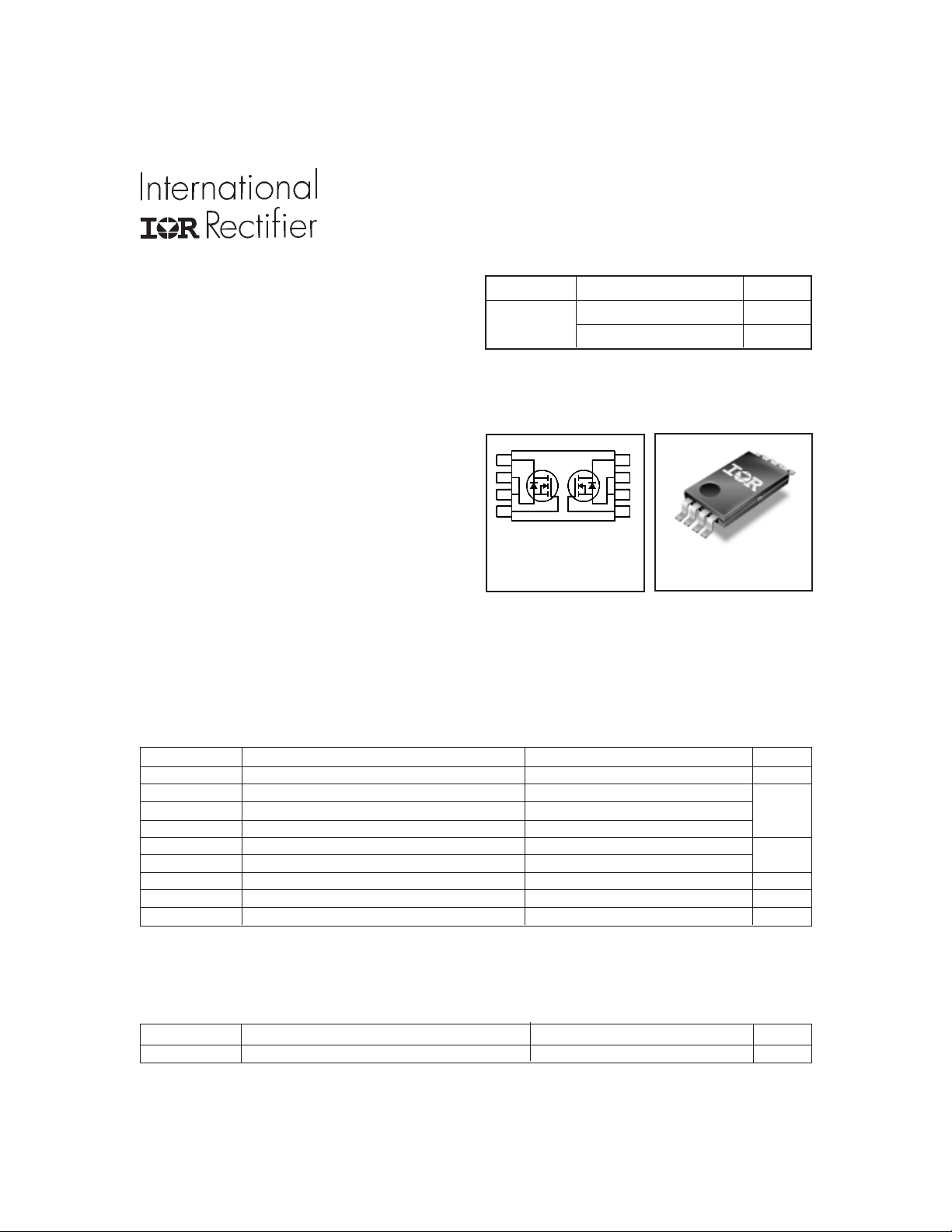
IRF7752
HEXFET® Power MOSFET
V
DSS
30V 0.030@VGS = 10V 4.6A
1
2
3
4
1 = D1
2 = S1
3 = S1
4 = G1
R
max I
DS(on)
0.036@VGS = 4.5V 3.9A
8
7
6
5
8 = D2
7 = S2
6 = S2
5 = G2
TSSOP-8
D
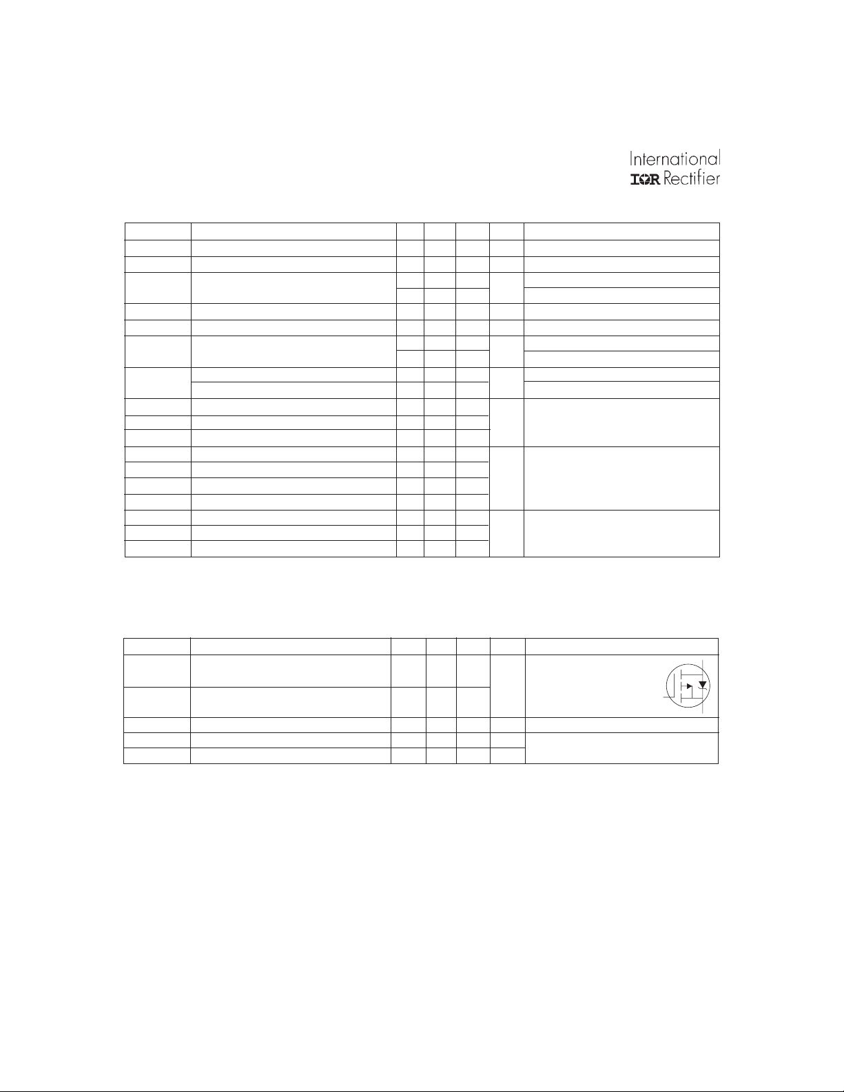
Absolute Maximum Ratings
Parameter Max. Units
V
DS
ID @ TC = 25°C Continuous Drain Current, VGS @ 10V ±4.6
ID @ TC = 70°C Continuous Drain Current, VGS @ 10V ±3.7 A
I
DM
PD @TA = 25°C Power Dissipation 1.0
PD @TA = 70°C Power Dissipation 0.64
V
GS
T
J, TSTG
Drain- Source Voltage 30 V
Pulsed Drain Current ±37
W
Linear Derating Factor 8.0 mW/°C
Gate-to-Source Voltage ± 12 V
Junction and Storage Temperature Range -55 to + 150 °C
Thermal Resistance
Parameter Max. Units
R
θJA
Maximum Junction-to-Ambient 125 °C/W
www.irf.com 1
3/25/01
Page 2
IRF7752
Electrical Characteristics @ TJ = 25°C (unless otherwise specified)
Parameter Min. Typ. Max. Units Conditions
V
(BR)DSS
∆V
(BR)DSS
R
DS(on)
V
GS(th)
g
fs
I
DSS
I
GSS
Q
g
Q
gs
Q
gd
t
d(on)
t
r
t
d(off)
t
f
C
iss
C
oss
C
rss
Drain-to-Source Breakdown Voltage 30 ––– ––– V VGS = 0V, ID = -250µA
/∆T
Breakdown Voltage Temp. Coefficient ––– 0.030 ––– V/°C Reference to 25°C, ID = 1mA
J
Static Drain-to-Source On-Resistance
––– ––– 0.030 VGS = 10V, ID = 4.6A
––– ––– 0.036 VGS = 4.5V, ID = 3.9A
Ω
Gate Threshold Voltage 0.60 ––– 2.0 V VDS = VGS, ID = 250µA
Forward Transconductance 12 ––– ––– S VDS = 10V, ID = 4.6A
Drain-to-Source Leakage Current
Gate-to-Source Forward Leakage ––– ––– -200 VGS = -12V
Gate-to-Source Reverse Leakage ––– ––– 200 VGS = 12V
––– ––– 20 VDS = 24V, VGS = 0V
––– ––– 100 VDS = 24V, VGS = 0V, TJ = 125°C
µA
nA
Total Gate Charge – – – 9 .0 ––– ID = 4.6A
Gate-to-Source Charge ––– 2.5 ––– nC VDS = 24V
Gate-to-Drain ("Miller") Charge ––– 2.6 ––– VGS = 4.5V
Turn-On Delay Time ––– 7. 2 ––– VDD = 15V
Rise Time ––– 9.1 ––– ID = 1.0A
Turn-Off Delay Time ––– 25 ––– RG = 6.0Ω
ns
Fall Time ––– 11 ––– VGS = 10V
Input Capacitance ––– 861 ––– VGS = 0V
Output Capacitance ––– 210 ––– pF VDS = 25V
Reverse Transfer Capacitance ––– 25 ––– ƒ = 1.0MHz
Source-Drain Ratings and Characteristics
Parameter Min. Typ. Max. Units Conditions
I
S
I
SM
V
SD
t
rr
Q
rr
Continuous Source Current MOSFET symbol
(Body Diode) showing the
Pulsed Source Current integral reverse
(Body Diode) p-n junction diode.
––– –––
––– ––– 37
0.91
A
G
Diode Forward Voltage ––– ––– 1.3 V TJ = 25°C, IS = 0.91A, VGS = 0V
Reverse Recovery Time ––– 25 ––– ns TJ = 25°C, IF = 0.91A
Reverse RecoveryCharge ––– 23 ––– nC di/dt = 100A/µs
Notes:
Repetitive rating; pulse width limited by
When mounted on 1 inch square copper board, t<10 sec
max. junction temperature.
Pulse width ≤ 300µs; duty cycle ≤ 2%.
2 www.irf.com
D
S
Page 3
IRF7752
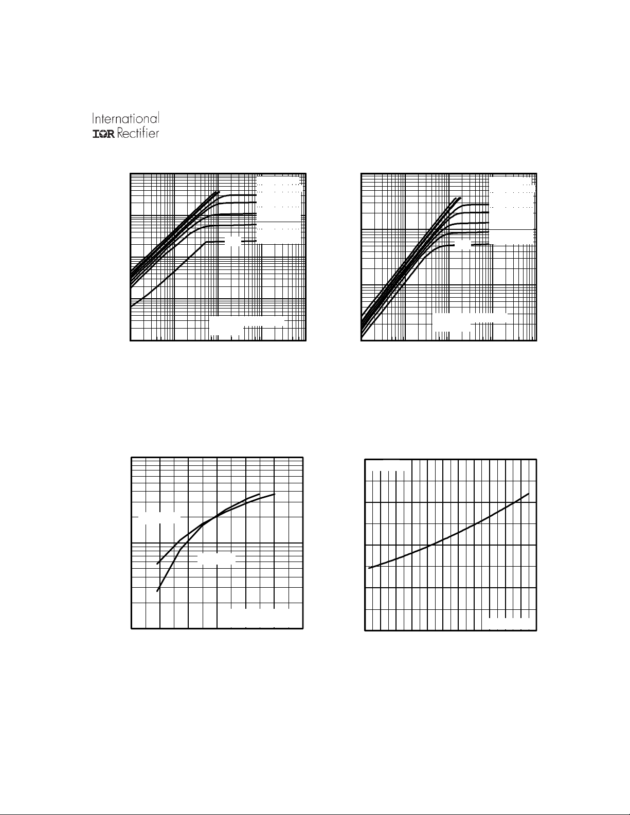
100
10
2.3V
1
0.1
, Drain-to-Source Current (A)
D
I
20µs PULSE WIDTH
Tj = 25°C
0.01
0.01 0.1 1 10 100
VDS, Drain-to-Source Voltage (V)
Fig 1. Typical Output Characteristics
100
VGS
TOP 10.0V
5.0V
4.5V
3.3V
3.0V
2.7V
2.5V
BOTTOM 2.3V
100
10
2.3V
1
, Drain-to-Source Current (A)
D
I
20µs PULSE WIDTH
Tj = 150°C
0.1
0.01 0.1 1 10 100
VDS, Drain-to-Source Voltage (V)
Fig 2. Typical Output Characteristics
2.0
4.6A
I =
D
VGS
TOP 10.0V
5.0V
4.5V
3.3V
3.0V
2.7V
2.5V
BOTTOM 2.3V
1.5
°
T = 150 C
J
10
°
T = 25 C
J
D
I , Drain-to-Source Current (A)
V = 15V
DS
1
2.0 2.3 2.7 3.0 3.3 3.7 4.0
V , Gate-to-Source Voltage (V)
GS
20µs PULSE WIDTH
Fig 3. Typical Transfer Characteristics
1.0
(Normalized)
0.5
DS(on)
R , Drain-to-Source On Resistance
0.0
-60 -40 -20 0 20 40 60 80 100 120 140 160
T , Junction Temperature( C)
J
Fig 4. Normalized On-Resistance
V =
GS
°
10V
Vs. Temperature
www.irf.com 3
Page 4

IRF7752
gsg
1400
1200
1000
800
600
C, Capacitance (pF)
400
200
0
1 10 100
V
=
0V,
GS
C
=
iss
C
=
rssgd
C
=
oss dsgd
C
iss
C
oss
C
rss
V , Drain-to-Source Voltage (V)
DS
f = 1MHz
C
+ C
C SHORTED
C
C
d , ds
+ C
Fig 5. Typical Capacitance Vs.
Drain-to-Source Voltage
100
10
I =
4.6A
D
8
6
4
2
GS
V , Gate-to-Source Voltage (V)
0
0 4 8 12 16 20
Q , Total Gate Charge (nC)
G
V = 24V
DS
V = 15V
DS
Fig 6. Typical Gate Charge Vs.
Gate-to-Source Voltage
1000
OPERATION IN THIS AREA LIMITED
BY R
DS(on)
°
T = 150 C
10
1
SD
I , Reverse Drain Current (A)
0.1
0.2 0.4 0.6 0.8 1.0 1.2 1.4
J
°
T = 25 C
J
V = 0 V
GS
V ,Source-to-Drain Voltage (V)
SD
Fig 7. Typical Source-Drain Diode
100
10
D
I , Drain Current (A)I , Drain Current (A)
1
°
= 25 C
C
T T= 150 C
Single Pulse
0.1
0.1 1 10 100
°
J
V , Drain-to-Source Voltage (V)
DS
Fig 8. Maximum Safe Operating Area
10us
100us
1ms
10ms
Forward Voltage
4 www.irf.com
Page 5

IRF7752
5.0
4.0
3.0
2.0
D
I , Drain Current (A)
1.0
0.0
25 50 75 100 125 150
T , Case Temperature( C)
C
°
Fig 9. Maximum Drain Current Vs.
Case Temperature
1000
R
D.U.T.
D
+
V
-
V
DS
V
GS
R
G
10V
Pulse Width ≤ 1 µs
Duty Factor ≤ 0.1 %
Fig 10a. Switching Time Test Circuit
V
DS
90%
10%
V
GS
t
d(on)tr
t
d(off)tf
Fig 10b. Switching Time Waveforms
DD
100
thJA
D = 0.50
0.20
0.10
10
0.05
P
0.02
0.01
1
Thermal Response (Z )
0.1
0.00001 0.0001 0.001 0.01 0.1 1 10 100
SINGLE PULSE
(THERMAL RESPONSE)
Notes:
1. Duty factor D =t / t
2. Peak T =P x Z + T
t , Rectangular Pulse Duration (sec)
1
J DM thJA A
DM
t
1 2
1
t
2
Fig 10. Maximum Effective Transient Thermal Impedance, Junction-to-Ambient
www.irf.com 5
Page 6

IRF7752
0.080
)
0.060
0.040
ID = 4.6A
0.020
, Drain-to -Source On Resistance (Ω
DS(on)
R
0.000
2.0 3.0 4.0 5.0 6.0 7.0 8.0 9.0 10.0
V
Gate -to -Source Voltage (V)
GS,
Fig 11. Typical On-Resistance Vs.
Gate Voltage
0.030
)
Ω
VGS = 4.5V
0.025
, Drain-to-Source On Resistance (
VGS = 10V
DS ( on )
R
0.020
0 5 10 15 20 25 30 35 40
ID , Drain Current ( A )
Fig 12. Typical On-Resistance Vs.
Drain Current
Current Regulator
Same Type as D.U.T.
Q
G
10 V
Q
GS
V
G
Q
GD
Charge
Fig 13a. Basic Gate Charge Waveform
12V
V
GS
Fig 13b. Gate Charge Test Circuit
50KΩ
.2µF
.3µF
3mA
Current Sampling Resistors
+
V
D.U.T.
I
G
DS
-
I
D
6 www.irf.com
Page 7

TSSOP-8 Package Outline
IRF7752
Data and specifications subject to change without notice.
This product has been designed and qualified for the Industrial market.
Qualification Standards can be found on IR’s Web site.
IR WORLD HEADQUARTERS: 233 Kansas St., El Segundo, California 90245, USA Tel: (310) 252-7105
TAC Fax: (310) 252-7903
Visit us at www.irf.com for sales contact information. 3/01
www.irf.com 7
 Loading...