

Page 1
l Ultra Low On-Resistance
l P-Channel MOSFET
l Very Small SOIC Package
l Low Profile (< 1.2mm)
l Available in Tape & Reel
Description
HEXFET
fier utilize advanced processing techniques to achieve
extremely low on-resistance per silicon area. This
benefit, combined with the ruggedized device design,
that International Rectifier is well known for, provides
the designer with an extremely efficient and reliable
device for battery and load management.
®
Power MOSFETs from International Recti-
PD -94064
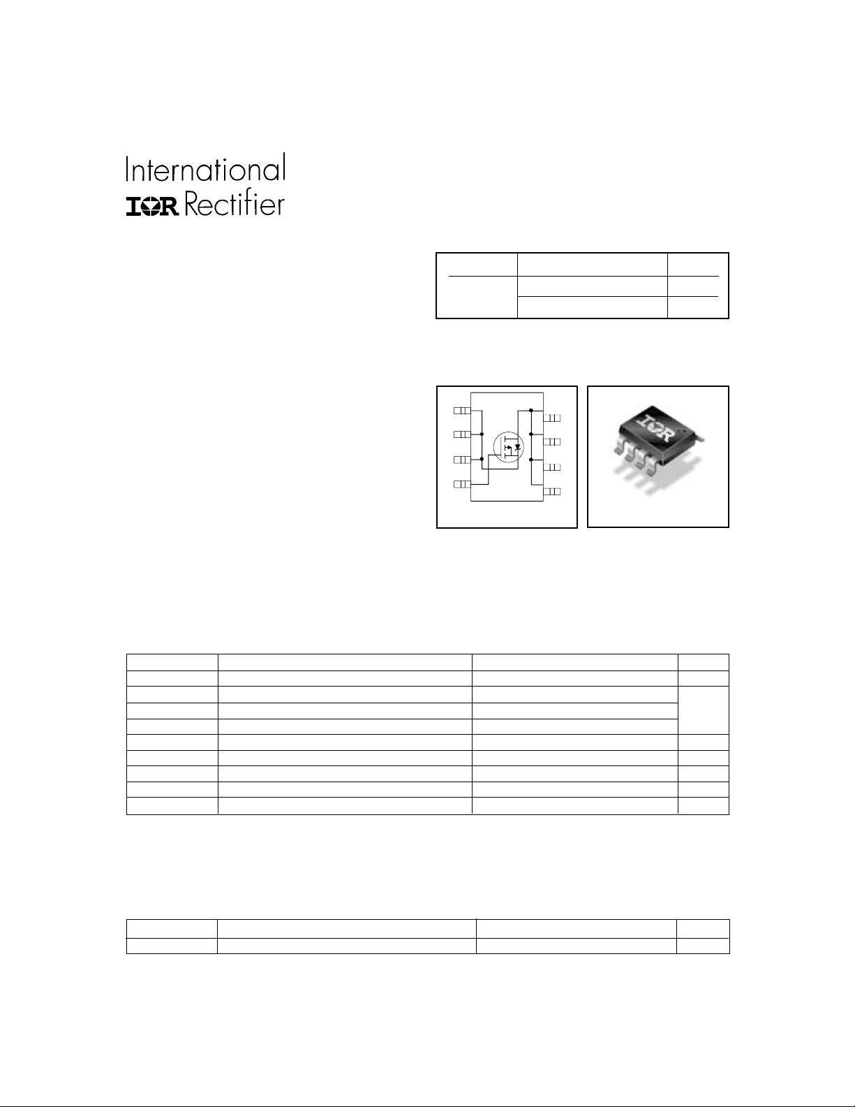
IRF7726
HEXFET® Power MOSFET
V
DSS
-30V 0.026@VGS = -10V -7.0A
1
S
2
S
3
S
4
R
max I
DS(on)
0.040@VGS = -4.5V -6.0A
A
8
D
7
D
6
D
5
DG
D
The new Micro8 package, with half the footprint area
Top V iew
MICRO-8
of the standard SO-8, provides the smallest footprint
available in an SOIC outline. This makes the Micro8
an ideal device for applications where printed circuit
board space is at a premium. The low profile (<1.2mm)
of the Micro8 will allow it to fit easily into extremely thin
application environments such as portable electronics
and PCMCIA cards.
Absolute Maximum Ratings
Parameter Max. Units
V
DS
ID @ TA = 25°C Continuous Drain Current, VGS @ -10V -7.0
ID @ TA = 70°C Continuous Drain Current, VGS @ -10V -5.7 A
I
DM
PD @TA = 25°C Maximum Power Dissipation 1.79 W
PD @TA = 70°C Maximum Power Dissipation 1.14 W
Linear Derating Factor 0.01 W/°C
V
GS
TJ , T
STG
Drain-Source Voltage -30 V
Pulsed Drain Current -28
Gate-to-Source Voltage ±20 V
Junction and Storage Temperature Range -55 to +150 °C
Thermal Resistance
Parameter Max. Units
R
θJA
Maximum Junction-to-Ambient 70 °C/W
www.irf.com 1
12/21/00
Page 2
IRF7726
Electrical Characteristics @ TJ = 25°C (unless otherwise specified)
Parameter Min. Typ. Max. Units Conditions
V
(BR)DSS
∆V
(BR)DSS
R
DS(on)
V
GS(th)
g
fs
I
DSS
I
GSS
Q
g
Q
gs
Q
gd
t
d(on)
t
r
t
d(off)
t
f
C
iss
C
oss
C
rss
Drain-to-Source Breakdown Voltage -30 ––– ––– VVGS = 0V, ID = -250µA
/∆T
Breakdown Voltage Temp. Coefficient ––– 0.016 ––– V/°C Reference to 25°C, ID = -1mA
J
Static Drain-to-Source On-Resistance
––– ––– 0.026 VGS = -10V, ID = -7.0A
––– ––– 0.040 VGS = -4.5V, ID = -6.0A
Ω
Gate Threshold Voltage -1.0 ––– -2.5 V VDS = VGS, ID = -250µA
Forward Transconductance 10 ––– ––– SVDS = -10V, ID = -7.0A
Drain-to-Source Leakage Current
Gate-to-Source Forward Leakage ––– ––– -100 VGS = -20V
Gate-to-Source Reverse Leakage ––– ––– 100 VGS = 20V
––– ––– -15 VDS = -24V, VGS = 0V
––– ––– -25 VDS = -24V, VGS = 0V, TJ = 70°C
µA
nA
Total Gate Charge ––– 46 69 ID = -7.0A
Gate-to-Source Charge ––– 8.0 ––– nC VDS = -15V
Gate-to-Drain ("Miller") Charge ––– 8.1 ––– VGS = -10V
Turn-On Delay Time ––– 15 23 VDD = -15V, VGS = -10V
Rise Time ––– 25 38 ID = -1.0A
Turn-Off Delay Time ––– 227 341 RG = 6.0Ω
ns
Fall Time ––– 107 161 RD = 15Ω
Input Capacitance ––– 2204 ––– VGS = 0V
Output Capacitance ––– 341 ––– pF VDS = -25V
Reverse Transfer Capacitance ––– 220 ––– ƒ = 1.0MHz
Source-Drain Ratings and Characteristics
Parameter Min. Typ. Max. Units Conditions
I
S
I
SM
V
SD
t
rr
Q
rr
Continuous Source Current MOSFET symbol
(Body Diode) showing the
Pulsed Source Current integral reverse
(Body Diode) p-n junction diode.
––– –––
–––
–––
-1.8
-28
A
G
Diode Forward Voltage ––– ––– -1.2 V TJ = 25°C, IS = -1.8A, VGS = 0V
Reverse Recovery Time ––– 35 53 ns TJ = 25°C, IF = -1.8A
Reverse Recovery Charge ––– 32 48 µC di/dt = -100A/µs
Notes:
Repetitive rating; pulse width limited by
When mounted on 1 inch square copper board, t < 10 sec.
max. junction temperature.
Pulse width ≤ 400µs; duty cycle ≤ 2%.
2 www.irf.com
D
S
Page 3

IRF7726
100
10
1
-2.5V
0.1
, Drain-to-Source Current (A)
D
-I
20µs PULSE WIDTH
Tj = 25°C
0.01
0.1 1 10 100
-VDS, Drain-to-Source Voltage (V)
Fig 1. Typical Output Characteristics
100
VGS
TOP -10.0V
-4.5V
-3.7V
-3.5V
-3.3V
-3.0V
-2.7V
BOTTOM -2.5V
100
10
-2.5V
1
, Drain-to-Source Current (A)
D
-I
20µs PULSE WIDTH
Tj = 150°C
0.1
0.1 1 10 100
-VDS, Drain-to-Source Voltage (V)
Fig 2. Typical Output Characteristics
2.0
-7.0A
I =
D
VGS
TOP -10.0V
-4.5V
-3.7V
-3.5V
-3.3V
-3.0V
-2.7V
BOTTOM -2.5V
°
T = 150 C
J
10
°
T = 25 C
1
D
-I , Drain-to-Source Current (A)
0.1
2.0 3.0 4.0 5.0 6.0
J
V = -15V
DS
20µs PULSE WIDTH
-V , Gate-to-Source Voltage (V)
GS
Fig 3. Typical Transfer Characteristics
1.5
1.0
(Normalized)
0.5
DS(on)
R , Drain-to-Source On Resistance
0.0
-60 -40 -20 0 20 40 60 80 100 120 140 160
T , Junction Temperature ( C)
J
Fig 4. Normalized On-Resistance
V =
GS
°
-10V
Vs. Temperature
www.irf.com 3
Page 4

IRF7726
)
3200
2800
2400
2000
1600
1200
C, Capacitance (pF)
800
400
0
1 10 100
V
=
0V,
GS
C
=
iss gs gd , ds
C
=
rss gd
C
=
oss ds gd
C
iss
C
oss
C
rss
-V , Drain-to-Source Voltage (V)
DS
f = 1MHz
C
+ C
C
C
C SHORTED
+ C
Fig 5. Typical Capacitance Vs.
Drain-to-Source Voltage
100
°
T = 25 C
J
16
I =
-7.0A
D
14
12
10
8
6
4
GS
-V , Gate-to-Source Voltage (V)
2
0
0 10 20 30 40 50 60
Q , Total Gate Charge (nC)
G
V =-24V
DS
V =-15V
DS
Fig 6. Typical Gate Charge Vs.
Gate-to-Source Voltage
100
OPERATION IN THIS AREA LIMITED
BY R
DS(on
°
T = 150 C
J
10
1
SD
-I , Reverse Drain Current (A)
V = 0 V
0.1
0.0 1.5 3.0 4.5 6.0
-V ,Source-to-Drain Voltage (V)
SD
GS
Fig 7. Typical Source-Drain Diode
10
D
-I , Drain Current (A)I , Drain Current (A)
°
= 25 C
C
T T= 150 C
Single Pulse
1
0.1 1 10 100
°
J
-V , Drain-to-Source Voltage (V)
DS
Fig 8. Maximum Safe Operating Area
100us
1ms
10ms
Forward Voltage
4 www.irf.com
Page 5

IRF7726
8.0
6.0
4.0
D
-I , Drain Current (A)
2.0
0.0
25 50 75 100 125 150
T , Case Temperature( C)
C
°
Fig 9. Maximum Drain Current Vs.
Case Temperature
100
R
D.U.T.
D
-
+
V
DS
V
GS
R
G
V
GS
Pulse Width ≤ 1 µs
Duty Factor ≤ 0.1 %
Fig 10a. Switching Time Test Circuit
V
GS
10%
90%
V
DS
t
d(on)tr
t
d(off)tf
Fig 10b. Switching Time Waveforms
V
DD
D = 0.50
thJA
Thermal Response (Z )
0.20
10
0.10
0.05
0.02
0.01
1
SINGLE PULSE
(THERMAL RESPONSE)
Notes:
1. Duty factor D = t / t
2. Peak T =P x Z + T
0.1
0.0001 0.001 0.01 0.1 1 10 100 1000
t , Rectangular Pulse Duration (sec)
1
J DM thJA A
P
DM
t
1 2
1
t
2
Fig 11. Maximum Effective Transient Thermal Impedance, Junction-to-Ambient
www.irf.com 5
Page 6

IRF7726
0.070
)
Ω
0.060
0.050
0.040
ID = -7.0A
0.030
, Drain-to -Source On Resistance (
0.020
DS(on)
R
0.010
2.0 3.0 4.0 5.0 6.0 7.0 8.0 9.0 10.0
-V
Gate -to -Source Voltage (V)
GS,
Fig 12. Typical On-Resistance Vs.
Gate Voltage
0.120
)
Ω
0.080
VGS = -4.5V
0.040
, Drain-to-Source On Resistance (
DS ( on )
R
0.000
0 102030405060
-ID , Drain Current ( A )
Fig 13. Typical On-Resistance Vs.
Drain Current
VGS = -10V
Current Regulator
Same Type as D.U.T.
50KΩ
.2µF
10 V
Q
G
Q
GS
V
G
Q
GD
12V
V
GS
.3µF
D.U.T.
-3mA
I
G
Current Sampling Resistors
I
V
DS
+
D
Charge
Fig 14a. Basic Gate Charge Waveform
Fig 14b. Gate Charge Test Circuit
6 www.irf.com
Page 7

IRF7726
2.4
2.1
( V )
1.8
GS(th)
-V
1.5
1.2
-75 -50 -25 0 25 50 75 100 125 150
TJ , Temperature ( °C )
ID = -250µA
Fig 15. Typical Vgs(th) Vs.
Junction Temperature
150
120
90
Power (W)
60
30
0
0.001 0.010 0.100 1.000 10.000 100.000
Time (sec)
Fig 16. Typical Power Vs. Time
www.irf.com 7
Page 8

IRF7726
Package Outline
Micro-8 Outline
Dimensions are shown in millimeters (inches)
D
3
- B -
3
- A -
- C B 8 X
NOTES:
1 DIMENSIONING AND TOLERANCING PER ANSI Y14.5M-1982.
2 CONTROLLING DIMENSION : INCH.
3 DIMENSIONS DO NOT INCLUDE MOLD FLASH.
8 7 6 5
E
0.2 5 (.01 0 ) M A M
1 2 3 4
e
6X
e 1
A
A 1
0.0 8 (.0 0 3 ) M C A S B S
H
0.10 (.004)
Part Mar king Information
LEAD ASSIGNMEN TS
D D D D D1 D1 D2 D2
8 7 6 5
SINGLE
1 2 3 4
S S S G
θ
8 7 6 5
DUAL
1 2 3 4
S1 G1 S2 G2
L
8X
8X
IN CHES M ILL IM E TERS
DIM
M IN M A X M IN MAX
A .0 3 6 .0 4 4 0.9 1 1 .1 1
A1 .0 0 4 .0 0 8 0.1 0 0 .2 0
B .0 1 0 .0 1 4 0.2 5 0 .3 6
C .005 .007 0.13 0.18
D .116 .120 2.95 3.05
e .0256 BASIC 0.65 BASIC
e1 .0128 BASIC 0.33 BASIC
E .1 1 6 .1 2 0 2.9 5 3 .0 5
H .188 .198 4.78 5 .03
L .0 1 6 .0 26 0 .4 1 0 .66
0 ° 6° 0 ° 6°
θ
RECOMMENDED FOOTPRINT
1.04
( .041 )
C
8X
3.20
( .126 )
0.38
( .015 )
4.24
( .167 )
0.65
( .0256 )
8X
6X
5.28
( .208 )
Micro-8
EXA M P L E : TH IS IS A N IR F 7 5 0 1
DATE CO DE (YW W)
Y = LAST D IGIT OF YEAR
W W = WEEK
451
7501
PART NUMBER
TOP
8 www.irf.com
A
Page 9

Tape & Reel Information
(
)
)
)
)
)
)
)
Micro-8
Dimensions are shown in millimeters (inches)
TERMINAL NUMBER 1
12.3 ( .484
11.7 ( .461
IRF7726
8.1 ( .318
7.9 ( .312
NOTES:
1. OUTLINE CON FOR M S TO EIA-481 & EIA-541.
2. CONTROLLING DIMENSION : M ILLIMETER.
330.00
12.992
MAX.
NOTES :
1. CONTR OLLING DIMENSIO N : MILLIMETER.
2. O U TLINE CONFO R MS TO EIA-481 & EIA-541.
Data and specifications subject to change without notice.
This product has been designed and qualified for the commercial market.
FEED DIRECTION
14.40 ( .566
12.40 ( .488
Qualification Standards can be found on IR’s Web site.
IR WORLD HEADQUARTERS: 233 Kansas St., El Segundo, California 90245, USA Tel: (310) 252-7105
TAC Fax: (310) 252-7903
Visit us at www.irf.com for sales contact information.12/00
www.irf.com 9
 Loading...