

Page 1

● Trench Technology
● Ultra Low On-Resistance
● P-Channel MOSFET
● Very Small SOIC Package
● Low Profile (<1.1mm)
● Available in Tape & Reel
Description
New trench HEXFET power MOSFETs from International
Rectifier utilize advanced processing techniques to achieve
extremely low on-resistance per silicon area. This benefit,
combined with the ruggedized device design that HEXFET
Power MOSFETs are well known for, provides the designer
with an extremely efficient and reliable device for use in a wide
variety of applications.
The new Micro8 package has half the footprint area of the
standard SO-8. This makes the Micro8 an ideal package for
applications where printed circuit board space is at a premium.
The low profile (<1.1mm) of the Micro8 will allow it to fit easily
into extremely thin application environments such as portable
electronics and PCMCIA cards.
S
S
S
1
2
3
4
Top V iew
PD-91866B
IRF7663
HEXFET® Power MOSFET
A
8
D
V
7
6
5
D
D
DG
R
MICRO8
DS(on)
= -20V
DSS
= 0.020Ω
Absolute Maximum Ratings
Parameter Max. Units
V
DS
ID @ TA = 25°C Continuous Drain Current, VGS @ -4.5V -8.2
ID @ TA= 70°C Continuous Drain Current, VGS @ -4.5V -6.6 A
I
DM
PD @TA = 25°C Power Dissipation 1.8
PD @TA = 70°C Power Dissipation 1.15
E
AS
V
GS
T
J, TSTG
Drain- Source Voltage -20 V
Pulsed Drain Current -66
W
Linear Derating Factor 10 mW/°C
Single Pulse Avalanche Energy 115 mJ
Gate-to-Source Voltage ± 12 V
Junction and Storage Temperature Range -55 to + 150 °C
Thermal Resistance
Parameter Max. Units
R
θJA
Maximum Junction-to-Ambient 70 °C/W
www.irf.com 1
5 /25/00
Page 2

IRF7663
Electrical Characteristics @ TJ = 25°C (unless otherwise specified)
Parameter Min. Typ. Max. Units Conditions
V
(BR)DSS
∆V
(BR)DSS
R
DS(on)
V
GS(th)
g
fs
I
DSS
I
GSS
Q
g
Q
gs
Q
gd
t
d(on)
t
r
t
d(off)
t
f
C
iss
C
oss
C
rss
Drain-to-Source Breakdown Voltage -20 ––– ––– V VGS = 0V, ID = -250uA
/∆T
Breakdown Voltage Temp. Coefficient ––– -0.01 ––– V/°C Reference to 25°C, ID = -1mA
J
Static Drain-to-Source On-Resistance
––– ––– 0.020 VGS = -4.5V, ID = -7.0A
––– ––– 0.040 VGS = -2.5V, ID = -5.1A
Ω
Gate Threshold Voltage -0.60 ––– -1.2 V VDS = VGS, ID = -250µA
Forward Transconductance 14.5 ––– ––– S VDS = -10V, ID = -7.0A
Drain-to-Source Leakage Current
Gate-to-Source Forward Leakage ––– ––– -100 VGS = -12V
Gate-to-Source Reverse Leakage ––– ––– 100 VGS = 12V
––– ––– -1.0 VDS = -16V, VGS = 0V
––– ––– -25 VDS = -16V, VGS = 0V, TJ = 70°C
µA
nA
Total Gate Charge ––– 30 4 5 ID = -6.0A
Gate-to-Source Charge ––– 5.0 7.5 nC VDS = -10V
Gate-to-Drain ("Miller") Charge ––– 7.0 10.5 VGS = -5.0V
Turn-On Delay Time ––– 11 ––– VDD = -10V
Rise Time ––– 100 ––– ID = -6.0A
Turn-Off Delay Time ––– 125 ––– RG = 6.2Ω
ns
Fall Time ––– 172 ––– RD = 1.64Ω
Input Capacitance ––– 2520 ––– VGS = 0V
Output Capacitance ––– 615 ––– pF VDS = -10V
Reverse Transfer Capacitance ––– 375 ––– ƒ = 1.0MHz
Source-Drain Ratings and Characteristics
Parameter Min. Typ. Max. Units Conditions
I
S
I
SM
V
SD
t
rr
Q
rr
Continuous Source Current MOSFET symbol
(Body Diode) showing the
Pulsed Source Current integral reverse
(Body Diode) p-n junction diode.
––– –––
-1.8
––– ––– -66
A
G
Diode Forward Voltage ––– ––– -1.2 V TJ = 25°C, IS = -7.0A, VGS = 0V
Reverse Recovery Time ––– 70 105 ns TJ = 25°C, IF = -2.5A
Reverse RecoveryCharge ––– 50 75 nC di/dt = 100A/µs
Notes:
Repetitive rating; pulse width limited by
When mounted on 1 inch square copper board, t<10 sec
max. junction temperature.
Pulse width ≤ 300µs; duty cycle ≤ 2%.
Starting T
RG = 25Ω, I
= 25°C, L = 17.8mH
J
= -3.6A. (See Figure 10)
AS
2 www.irf.com
D
S
Page 3
IRF7663
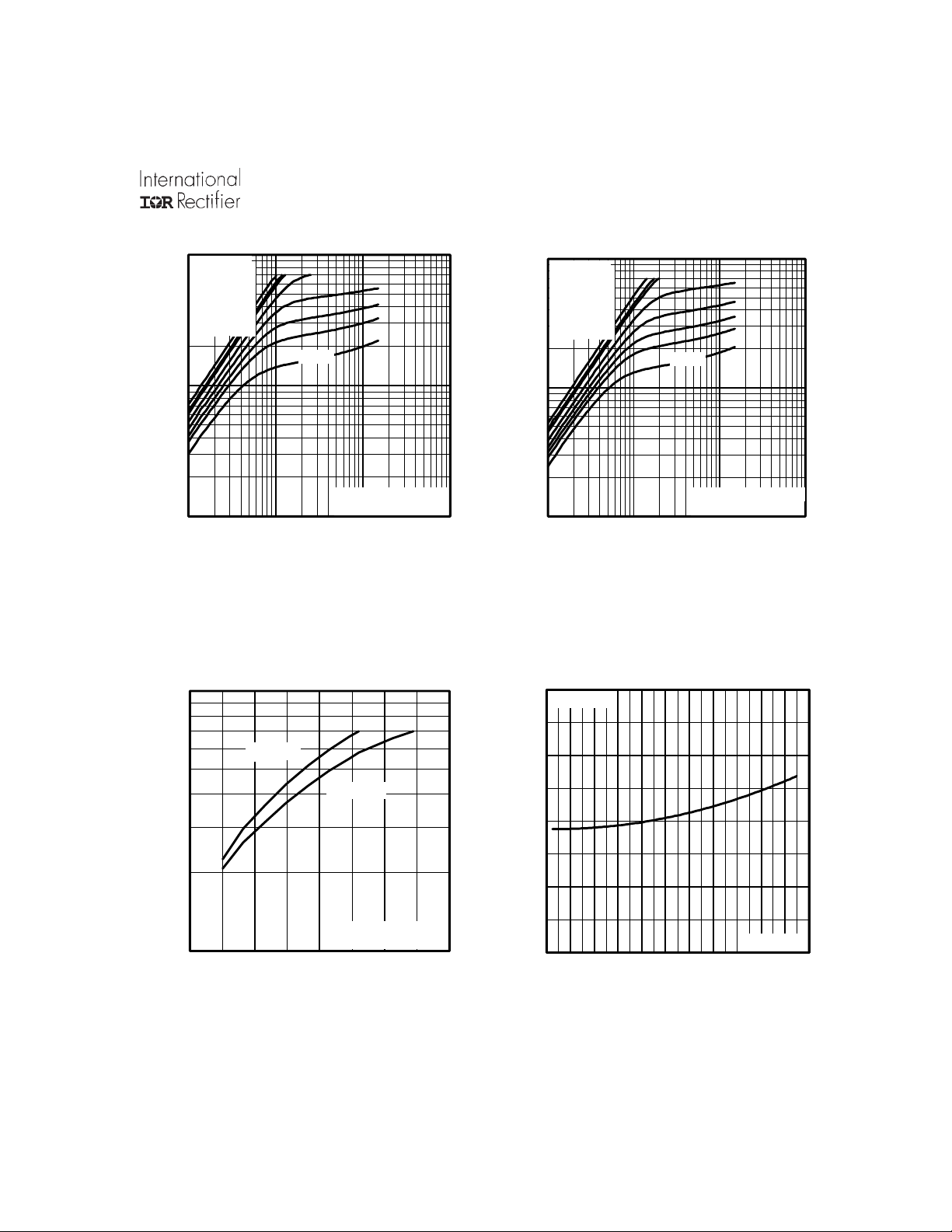
100
TOP
BOTTOM
VGS
-7.00V
-5.00V
-4.50V
-3.50V
-3.00V
-2.70V
-2.50V
-2.25V
-2.25V
10
D
-I , Drain-to-Source Current (A)
20µs PULSE WIDTH
°
T = 25 C
1
0.1 1 10 100
-V , Drain-to-Source Voltage (V)
DS
J
Fig 1. Typical Output Characteristics
100
100
TOP
BOTTOM
VGS
-7.00V
-5.00V
-4.50V
-3.50V
-3.00V
-2.70V
-2.50V
-2.25V
-2.25V
10
D
-I , Drain-to-Source Current (A)
20µs PULSE WIDTH
°
T = 150 C
1
0.1 1 10 100
-V , Drain-to-Source Voltage (V)
DS
J
Fig 2. Typical Output Characteristics
2.0
I =
D
-8.2A
°
T = 25 C
J
°
T = 150 C
J
1.5
1.0
(Normalized)
D
-I , Drain-to-Source Current (A)
V = -15V
DS
10
2.0 2.5 3.0 3.5 4.0
-V , Gate-to-Source Voltage (V)
GS
20µs PULSE WIDTH
Fig 3. Typical Transfer Characteristics
0.5
DS(on)
R , Drain-to-Source On Resistance
0.0
-60 -40 -20 0 20 40 60 80 100 120 140 160
T , Junction Temperature( C)
J
Fig 4. Normalized On-Resistance
V =
GS
°
-4.5V
Vs. Temperature
www.irf.com 3
Page 4

IRF7663
4000
3000
V
= 0V, f = 1 MHZ
GS
C
= C
iss
gs
C
= C
rss
gd
C
= C
ds
+ C
oss
+ Cgd, C
gd
Ciss
2000
C, Capacitance(pF)
1000
Coss
Crss
0
1 10 100
-VDS, Drain-to-Source Voltage (V)
Fig 5. Typical Capacitance Vs.
Drain-to-Source Voltage
100
SHORTED
ds
10
I =
-6.0A
GS
D
8
6
4
2
V =-10V
DS
-V , Gate-to-Source Voltage (V)
FOR TEST CIRCUIT
0
0 10 20 30 40 50
Q , Total Gate Charge (nC)
G
SEE FIGURE
Fig 6. Typical Gate Charge Vs.
Gate-to-Source Voltage
1000
OPERATION IN THIS AREA LIMITED
BY R
DS(on)
13
°
T = 25 C
J
100
T = 150 C
10
SD
-I , Reverse Drain Current (A)
1
0.5 1.0 1.5 2.0 2.5
-V ,Source-to-Drain Voltage (V)
SD
J
V = 0 V
GS
Fig 7. Typical Source-Drain Diode
°
10
D
-I , Drain Current (A)I , Drain Current (A)
°
= 25 C
C
T T= 150 C
Single Pulse
1
0.1 1 10 100
°
J
-V , Drain-to-Source Voltage (V)
DS
Fig 8. Maximum Safe Operating Area
10us
100us
1ms
10ms
Forward Voltage
4 www.irf.com
Page 5

IRF7663
(
)
9.0
7.5
6.0
4.5
3.0
D
-I , Drain Current (A)
1.5
0.0
25 50 75 100 125 150
T , Case Temperature ( C)
C
°
Fig 9. Maximum Drain Current Vs.
Case Temperature
100
300
TOP
240
180
120
60
AS
E , Single Pulse Avalanche Energy (mJ)
0
25 50 75 100 125 150
Starting T , Junction Temperature ( C)
J
BOTTOM
Fig 10. Maximum Avalanche Energy
Vs. Drain Current
I
D
-1.6A
-2.9A
-3.6A
°
D = 0.50
thJC
0.20
10
0.10
0.05
0.02
1
0.01
Thermal Response (Z )
0.1
0.00001 0.0001 0.001 0.01 0.1 1 10 100
SINGLE PULSE
THERMAL RESPONSE
Notes:
1. Duty factor D = t / t
2. Peak T = P x Z + T
t , Rectangular Pulse Duration (sec)
1
J DM thJC C
1 2
P
DM
t
1
t
2
Fig 11. Maximum Effective Transient Thermal Impedance, Junction-to-Ambient
www.irf.com 5
Page 6

IRF7663
Pac kage Outline
Micro8
Dimensions are shown in millimeters (inches)
D
3
- B -
3
- A -
- C B 8 X
NOTES:
1 DIMENSIONING AND TOLERANCING PER AN SI Y14.5M -1982.
2 CONTROLLING DIMEN SION : INCH.
3 DIMENSIONS DO NOT INCLUDE MOLD FLASH.
8 7 6 5
E
0.2 5 (.01 0 ) M A M
1 2 3 4
e
6X
e 1
A
A 1
0.0 8 (.0 0 3 ) M C A S B S
H
P art Marking Information
0.10 (.004)
LEAD ASSIGN MEN TS
D D D D D1 D1 D2 D2
8 7 6 5
SING LE
1 2 3 4
S S S G
θ
8 7 6 5
DUAL
1 2 3 4
S1 G1 S2 G2
L
8X
C
8X
IN CHE S M ILL IM ET E R S
DIM
M IN M AX M IN M A X
A .0 3 6 .0 4 4 0 .9 1 1 .1 1
A1 .0 0 4 .0 0 8 0 .1 0 0 .2 0
B .0 1 0 .0 1 4 0 .2 5 0 .3 6
C .005 .007 0.13 0.18
D .116 .120 2.95 3.05
e .0256 BASIC 0.65 BASIC
e1 .0128 BASIC 0.33 BASIC
E .1 1 6 .1 2 0 2 .9 5 3 .0 5
H .188 .198 4.78 5 .03
L .0 1 6 .0 2 6 0 .4 1 0 .6 6
0 ° 6° 0 ° 6 °
θ
RECOMMENDED FOOTPRINT
1.04
( .041 )
8X
3.20
( .126 )
0.38
( .015 )
4.24
( .167 )
0.65
( .0256 )
8X
6X
5.28
( .208 )
Micro8
EXAMPLE : THIS IS AN IRF750 1
DATE CO DE (YW W)
Y = LAST D IGIT OF YEAR
W W = WEEK
451
7501
PART NUMBER
TOP
6 www.irf.com
A
Page 7

Tape & Reel Inf ormation
Micro8
Dimensions are shown in millimeters (inches)
T ERM IN A L NUM BER 1
12.3 ( .484 )
11.7 ( .461 )
IRF7663
8.1 ( .318 )
7.9 ( .312 )
NOT ES:
1. OUTLINE CONFOR M S TO EIA-481 & EIA-541.
2. CONTROLLING DIMENSION : M ILLIMETER.
330.00
(12.992)
MAX.
NOTES :
1. CONTROLLING DIMENSION : MILLIMETER.
2. O U TLINE C O NFO R M S TO EIA-481 & EIA-541.
FEED DIRECTION
14.40 ( .566 )
12.40 ( .488 )
WORLD HEADQUARTERS: 233 Kansas St., El Segundo, California 90245, Tel: (310) 322 3331
IR GREAT BRITAIN: Hurst Green, Oxted, Surrey RH8 9BB, UK Tel: ++ 44 1883 732020
IR CANADA: 15 Lincoln Court, Brampton, Ontario L6T3Z2, Tel: (905) 453 2200
IR GERMANY: Saalburgstrasse 157, 61350 Bad Homburg Tel: ++ 49 6172 96590
IR ITALY: Via Liguria 49, 10071 Borgaro, Torino Tel: ++ 39 11 451 0111
IR FAR EAST: K&H Bldg., 2F, 30-4 Nishi-Ikebukuro 3-Chome, Toshima-Ku, Tokyo Japan 171 Tel: 81 3 3983 0086
IR SOUTHEAST ASIA: 1 Kim Seng Promenade, Great World City West Tower, 13-11, Singapore 237994 Tel: ++ 65 838 4630
IR TAIWAN:16 Fl. Suite D. 207, Sec. 2, Tun Haw South Road, Taipei, 10673, Taiwan Tel: 886-2-2377-9936
http://www.irf.com/ Data and specifications subject to change without notice. 5/00
www.irf.com 7
 Loading...