

Page 1

PD - 91269I
IRF7507
HEXFET® Power MOSFET
l Generation V Technology
l Ultra Low On-Resistance
l Dual N and P Channel MOSFET
l Very Small SOIC Package
l Low Profile (<1.1mm)
l Available in Tape & Reel
l Fast Switching
S1
G1
S2
G2
N-CHANNEL MOSFET
1
2
3
4
P-CHANNEL MOSFET
Top View
8
D1
7
D1
6
D2
5
D2
V
R
DS(on)
DSS
N-Ch P-Ch
20V -20V
0.135Ω 0.27Ω
Description
Fifth Generation HEXFETs from International Rectifier utilize advanced
processing techniques to achieve extremely low on-resistance per silicon
area. This benefit, combined with the fast switching speed and ruggedized
device design that HEXFET Power MOSFETs are well known for, provides the
designer with an extremely efficient and reliable device for use in a wide variety
of applications.
The new Micro8 package, with half the footprint area of the standard SO-8,
provides the smallest footprint available in an SOIC outline. This makes the
Micro8
Micro8 an ideal device for applications where printed circuit board space is at
a premium. The low profile (<1.1mm) of the Micro8 will allow it to fit easily into
extremely thin application environments such as portable electronics and
PCMCIA cards.
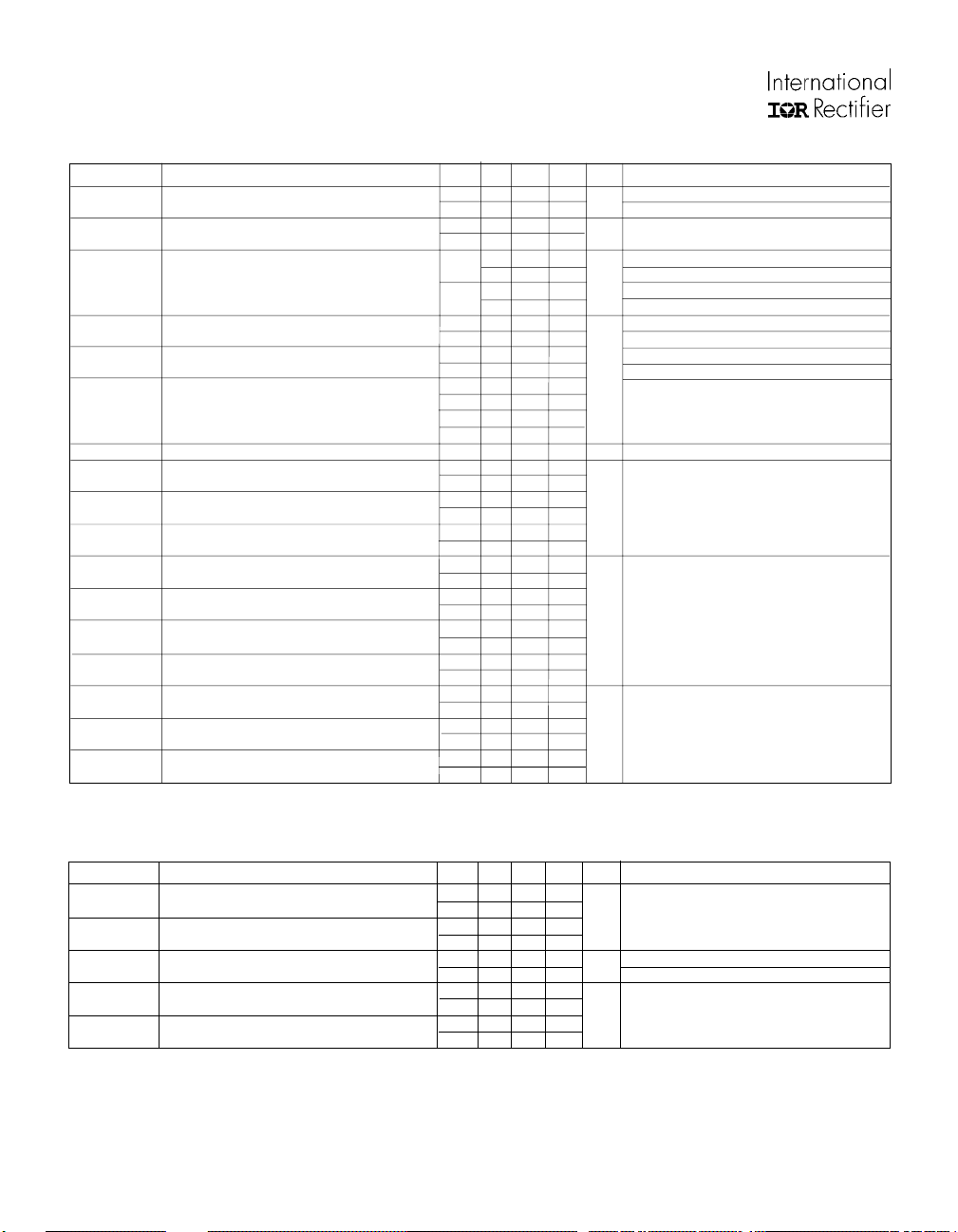
Absolute Maximum Ratings
Parameter Max. Units
N-Channel P-Channel
V
DS
ID @ TA = 25°C Continuous Drain Current, VGS 2.4 -1.7
ID @ TA = 70°C Continuous Drain Current, VGS 1.9 -1.4 A
I
DM
PD @TA = 25°C Maximum Power Dissipation 1.25 W
PD @TA = 70°C Maximum Power Dissipation 0.8 W
Linear Derating Factor 10 mW/°C
V
GS
V
GSM
dv/d t Peak Diode Recovery dv/dt 5.0 -5.0 V/ns
TJ , T
STG
Soldering Temperature, for 10 seconds 240 (1.6mm from case)
Drain-Source Voltage 20 -20 V
Pulsed Drain Current 19 -14
Gate-to-Source Voltage ± 12 V
Gate-to-Source Voltage Single Pulse tp<10µS 16 V
Junction and Storage Temperature Range -55 to + 150 °C
Thermal Resistance
Parameter Max. Units
R
θJA
Maximum Junction-to-Ambient 100 °C/W
www.irf.com 1
12/1/98
Page 2
IRF7507
Electrical Characteristics @ TJ = 25°C (unless otherwise specified)
t
V
∆V
R
V
g
I
I
Q
Q
Q
t
t
t
C
C
C
DSS
GSS
d(on)
r
d(off)
f
Parameter Min. Typ. Max. Units Conditions
(BR)DSS
(BR)DSS
DS(ON)
GS(th)
fs
Drain-to-Source Breakdown Voltage
/∆TJBreakdown Voltage Temp. Coefficient
Static Drain-to-Source On-Resistance
Gate Threshold Voltage
Forward Transconductance
Drain-to-Source Leakage Current
Gate-to-Source Forward Leakage N- P –– — ±100 VGS = ± 12V
g
gs
gd
Total Gate Charge
Gate-to-Source Charge
Gate-to-Drain ("Miller") Charge
Turn-On Delay Time
Rise Time
Turn-Off Delay Time
Fall Time
iss
oss
rss
Input Capacitance
Output Capacitance
Reverse Transfer Capacitance
N-Ch 20 — — V
P-Ch -20 — — V
N-Ch — 0.041 — Reference to 25°C, ID = 1mA
P-Ch — -0.012 — Reference to 25°C, I
— 0.085 0.14 V
N-Ch
— 0.120 0.20 VGS = 2.7V, ID = 0.85A
— 0.17 0.27 VGS = -4.5V, ID =-1.2A
P-Ch
— 0.28 0.40 VGS = -2.7V, ID =-0.6A
V/°C
N-Ch 0.7 — — VDS = VGS, ID = 250µA
P-Ch -0.7 — — V
N-Ch 2.6 — — V
P-Ch 1.3 — — VDS = -10V, ID = -0.6A
N-Ch — — 1.0 VDS = 16V, VGS = 0V
P-Ch — — -1.0 V
N-Ch — — 25 VDS = 16V, VGS = 0V, TJ = 125°C
µA
P-Ch — — -25 V
N-Ch –– 5.3 8.0
P-Ch — 5.4 8.2
N-Ch –– 0.84 1.3
P-Ch — 0.96 1.4
nC
N-Ch –– 2.2 3.3
P-Ch — 2.4 3.6
N-Ch — 5.7 —
P-Ch — 9.1 —
N-Ch — 24 —
P-Ch — 35 —
N-Ch — 15 —
ns
P-Ch — 38 —
N-Ch — 16 —
P-Ch — 43 —
N-Ch — 260 —
P-Ch — 240 —
N-Ch — 130 — pF
P-Ch — 130 —
N-Ch — 61 —
P-Ch — 64 —
= 0V, ID = 250µA
GS
V
= 0V, ID = -250µA
GS
= 4.5V, ID = 1.7A
GS
Ω
V
= VGS, ID = -250µA
DS
= 10V, ID = 0.85A
DS
S
= -16V, VGS = 0V
DS
= -16V, VGS = 0V, TJ = 125°C
DS
N-Channel
I
= 1.7A, VDS = 16V, VGS = 4.5V
D
P-Channel
I
= -1.2A, VDS = -16V, VGS = -4.5V
D
N-Channel
= 10V, ID = 1.7A, RG = 6.0Ω,
V
DD
RD = 5.7Ω
P-Channel
V
= -10V, ID = -1.2A, RG = 6.0Ω,
DD
RD = 8.3Ω
N-Channel
VGS = 0V, VDS = 15V, ƒ = 1.0MHz
P-Channel
V
= 0V, VDS = -15V, ƒ = 1.0MHz
GS
= -1mA
D
Source-Drain Ratings and Characteristics
Parameter Min. Typ. Max. Units Conditions
I
S
I
SM
V
SD
t
rr
Q
rr
Continuous Source Current (Body Diode)
Pulsed Source Current (Body Diode)
Diode Forward Voltage
Reverse Recovery Time
Reverse Recovery Charge
Notes:
Repetitive rating; pulse width limited by
max. junction temperature. ( See fig. 21 )
N-Channel I
P-Channel I
≤ 1.7A, di/dt ≤ 66A/µs, V
SD
≤ -1.2A, di/dt ≤ 100A/µs, V
SD
DD
DD
≤ V
≤ V
N-Ch — — 1.25
P-Ch — — -1.25
N-Ch — — 19
A
P-Ch — — -14
N-Ch — — 1.2 T
P-Ch — — -1.2 TJ = 25°C, IS = -1.2A, VGS = 0V
N-Ch — 39 59
P-Ch — 52 78
N-Ch — 37 56
P-Ch — 63 95
= 25°C, IS = 1.7A, VGS = 0V
J
V
N-Channel
ns
T
= 25°C, IF = 1.7A, di/dt = 100A/µs
J
P-Channel
nC
TJ = 25°C, IF = -1.2A, di/dt = -100A/µs
Pulse width ≤ 300µs; duty cycle ≤ 2%.
(BR)DSS
(BR)DSS
, TJ ≤ 150°C
, TJ ≤ 150°C
Surface mounted on FR-4 board, t ≤ 10sec.
2 www.irf.com
Page 3

100
A
A
A
A
A
A
10
VGS
TOP 7.5V
5.0V
4.0V
3.5V
3.0V
2.5V
2.0V
BOTTOM 1.5V
N - Channel
100
10
VGS
TOP 7.5V
5.0V
4.0V
3.5V
3.0V
2.5V
2.0V
BOTTOM 1.5V
IRF7507
1
0.1
D
I , Dra in-to -S ou rc e C ur re nt (A )
0.01
0.1 1 1 0
V , Drain-to-Source Voltage (V)
DS
1.5V
20µs PULS E W IDTH
T = 2 5 °C
J
Fig 1. Typical Output Characteristics
100
10
T = 150°C
J
T = 25°C
1
D
I , Drain-to-Source Current (A)
0.1
1.5 2.0 2.5 3.0 3.5 4.0
J
V = 10 V
DS
20µs PULSE WIDTH
V , Gate-to-Source Voltage (V)
GS
Fig 3. Typical Transfer Characteristics
1
1.5V
0.1
D
I , Dra in-to -S ou rc e Cu rren t (A )
0.01
0.1 1 1 0
V , Drain-to-Source Voltage (V)
DS
20µs PULS E WIDTH
T = 15 0 ° C
J
Fig 2. Typical Output Characteristics
100
10
T = 150°C
J
1
SD
I , Reverse D rain Current (A)
0.1
0.4 0.6 0.8 1.0 1.2 1.4 1.6 1.8
T = 25°C
J
V = 0V
GS
V , S o urc e-to-Drain V o ltage (V )
SD
Fig 4. Typical Source-Drain Diode
Forward Voltage
DS(on)
R , D ra in-to -S o u rc e O n R e si sta n ce
www.irf.com 3
2.0
I = 1.7A
D
1.5
1.0
(Normalized)
0.5
V = 4 .5V
0.0
-60 -40 -20 0 20 40 60 80 100 120 140 160
T , Junction Tem perature (°C)
J
GS
Fig 5. Normalized On-Resistance
Vs. Temperature
0.8
0.6
0.4
V = 2.5V
0.2
, Drain-to-Source On Resistance
DS(on)
R
V = 5 .0V
GS
0.0
0246
GS
I , Drain Current (A)
D
Fig 6. Typical On-Resistance Vs. Drain
Current
Page 4

IRF7507
A
A
g
g
g
A
(Ω
0.13
0.11
0.09
0.07
0.05
DS(on)
2345678
R , D rain- to -S o u rc e O n R e s is ta nc e
V , Gate -to -So urc e V o lta g e (V )
GS
I = 2 .4A
D
N - Channel
100
OPERATION IN THIS AREA LIMITED
10
1
D
I , Drain Current (A)I , Drain Current (A)
= 25 C
C
T T= 150 C
J
Single Pulse
0.1
1 10 100
V , Drain-to-Source Voltage (V)
DS
BY R
DS(on)
10us
100us
1ms
10ms
°
°
Fig 7. Typical On-Resistance Vs. Gate
Voltage
500
400
300
200
C, Capacitance (pF)
100
0
V = 0 V, f = 1 MH z
GS
C = C + C , C S HO R TE D
s gd d s
iss
C = C
d
rss
C = C + C
oss d s
C
iss
C
oss
C
rss
1 10 100
V , D ra in-to -S o ur ce V o ltage (V)
DS
d
Fig 9. Typical Capacitance Vs.
Drain-to-Source Voltage
Fig 8. Maximum Safe Operating Area
10
I = 1 .7 A
D
V = 16 V
DS
8
6
4
2
GS
-V , Gate-to-Source Voltage (V)
0
0246810
Q , T o tal G a te C h a rg e (n C)
G
FOR T E S T C IRCUIT
SEE F IGU R E 9
Fig 10. Typical Gate Charge Vs.
Gate-to-Source Voltage
4 www.irf.com
Page 5

100
A
A
A
A
A
VGS
TOP - 7.5V
- 5.0V
- 4.0V
- 3.5V
- 3.0V
- 2.5V
- 2.0V
10
BOTTOM - 1.5V
P - Channel
100
10
VGS
TOP - 7.5V
- 5.0V
- 4.0V
- 3.5V
- 3.0V
- 2.5V
- 2.0V
BOTTOM - 1.5V
IRF7507
1
0.1
D
-I , Drain-to-Source Current (A)
0.01
0.1 1 10
-1.5V
20µs PULSE W IDTH
T = 25°C
J
-V , Drain-to-Source Voltage (V)
DS
Fig 11. Typical Output Characteristics
10
T = 25°C
J
T = 15 0°C
J
1
0.1
D
-I , Drain-to-Source Current (A)
0.01
1.5 2.0 2.5 3.0 3.5 4.0 4.5 5.0
-V , Gate-to-Source Voltage (V)
GS
V = -10 V
DS
20µs PULSE W IDTH
Fig 13. Typical Transfer Characteristics
2.0
I = -1.2 A
D
1
0.1
D
-I , Drain-to-S ourc e C u rrent (A )
0.01
0.1 1 1 0
-V , Drain -to -S o ur ce V o lta ge (V )
DS
-1.5V
20µs PULS E W IDTH
T = 150°C
J
Fig 12. Typical Output Characteristics
10
T = 150°C
J
1
T = 25°C
J
0.1
SD
-I , Reverse D rain Current (A)
V = 0V
0.01
0.4 0.6 0.8 1.0 1.2
-V , Source-to-Drain Voltage (V)
SD
GS
Fig 14. Typical Source-Drain Diode
Forward Voltage
1.0
1.5
1.0
(Normalized)
0.5
DS(on)
R , Drain -to-S o ur ce O n R es ista nc e
0.0
-60 -40 -20 0 20 40 60 80 100 120 140 160
T , Junction Temperature (°C)
J
V = -4 .5 V
GS
Fig 15. Normalized On-Resistance
Vs. Temperature
Fig 16. Typical On-Resistance Vs. Drain
0.8
0.6
VGS = -2.5V
0.4
VGS = -5.0V
0.2
DS (on)
0.0
R , Drain-to-Source On Resistance
0.0 0.5 1.0 1.5 2.0
-I , Drain Current (A)
D
Current
www.irf.com 5
Page 6

IRF7507
A
g
g
g
A
0.300
0.250
0.200
0.150
DS (on)
0.100
R , Drain-to-Source On Resistance
2 3 4 5 6 7 8
-V , Gate-to-Source Voltage (V)
GS
ID = -1.7A
Fig 17. Typical On-Resistance Vs. Gate
Voltage
500
400
300
200
C, Capacitance (pF)
100
0
V = 0V , f = 1M Hz
GS
C = C + C , C S HOR T E D
s gd d s
iss
C = C
d
rss
C = C + C
oss d s
C
iss
C
oss
C
rss
1 10 100
-V , Dra in- to -S o u rc e Voltage (V)
DS
d
Fig 19. Typical Capacitance Vs.
Drain-to-Source Voltage
1000
P - Channel
N-P - Channel
100
OPERATION IN THIS AREA LIMITED
10
1
D
-I , Drain Current (A)I , Drain Current (A)
= 25 C
C
T T= 150 C
J
Single Pulse
0.1
1 10 100
-V , Drain-to-Source Voltage (V)
BY R
DS(on)
100us
1ms
10ms
°
°
DS
Fig 18. Maximum Safe Operating Area
10
I = -1.2A
D
V = -16V
DS
8
6
4
2
GS
-V , G a te- to-Sou rce Voltag e (V )
0
0246810
Q , T o ta l G a te C h a r g e (n C )
G
FOR TEST CIRCUIT
SEE FIGURE 19
Fig 20. Typical Gate Charge Vs.
Gate-to-Source Voltage
100
thJA
D = 0.50
0.20
0.10
10
0.05
0.02
0.01
1
Thermal Response (Z )
0.1
0.00001 0.0001 0.001 0.01 0.1 1 10 100
SINGLE PULSE
(THERMAL RESPONSE)
1. Duty factor D = t / t
2. Peak T =P x Z + T
t , Rectangular Pulse Duration (sec)
1
Notes:
P
DM
1 2
J DM thJA A
t
1
t
2
Fig 21. Maximum Effective Transient Thermal Impedance, Junction-to-Ambient
6 www.irf.com
Page 7

Package Outline
Micro8 Outline
Dimensions are shown in millimeters (inches)
IRF7507
D
3
- B -
3
- A -
- C B 8X
NOTES:
1 DIMENSIONING AND TOLERANCING PER ANSI Y14.5M-1982.
2 C O N T R O LLIN G D IM E N S ION : IN C H .
3 DIMENSIONS DO NOT INCLUDE MOLD FLASH.
8 7 6 5
E
0.25 (.0 1 0 ) M A M
1 2 3 4
e
6X
e 1
A
A 1
0.0 8 (.0 03) M C A S B S
H
Part Marking Information
Micro8
0.10 (.004)
LEAD ASSIGNMENTS
D D D D D1 D1 D2 D2
8 7 6 5
SINGLE
1 2 3 4
S S S G
θ
8 7 6 5
DUAL
1 2 3 4
S1 G1 S2 G 2
L
8X
8X
INCH E S MILL IMETERS
DIM
M IN MA X MIN MA X
A .036 .0 4 4 0 .9 1 1 .1 1
A1 .004 .0 0 8 0 .1 0 0 .2 0
B .010 .0 1 4 0 .2 5 0 .3 6
C .0 0 5 .0 0 7 0 .1 3 0 .1 8
D .1 1 6 .1 2 0 2 .9 5 3 .0 5
e .025 6 BAS IC 0 .6 5 B A SIC
e1 .012 8 BAS IC 0 .3 3 B A SIC
E .116 .1 2 0 2 .9 5 3.05
H .1 8 8 .1 9 8 4 .7 8 5 .0 3
L .016 .0 26 0 .4 1 0 .6 6
0° 6 ° 0 ° 6°
θ
RECOMMENDED FOOTPRINT
1.04
( .041 )
C
8X
3.20
( .12 6 )
0.38
( .015 )
4.24
( .167 )
0.65
( .0256 )
6X
8X
5.28
( .208 )
EXAMPLE : THIS IS AN IRF7501
DATE CODE (YW W)
Y = LAS T D IGIT OF Y E A R
WW = WEEK
451
7501
PART NUMBER
TOP
www.irf.com 7
A
Page 8

IRF7507
Tape & Reel Information
Micro8
Dimensions are shown in millimeters (inches)
TERMINAL NUMBER 1
12.3 ( .484 )
11.7 ( .461 )
8.1 ( .318 )
7.9 ( .312 )
NOTES:
1. OUTLINE CONFORMS TO EIA-481 & EIA-541.
2. CONTROLLING DIMENSION : MILLIMETER.
330.00
(12.992)
MAX.
NOTES :
1. CO NTRO LLING DIMENSION : MILLIMETER.
2. OUTLINE CONFORMS TO EIA-481 & EIA-541.
FEED DIRECTION
14.40 ( .566 )
12.40 ( .488 )
WORLD HEADQUARTERS: 233 Kansas St., El Segundo, California 90245, Tel: (310) 322 3331
IR GREAT BRITAIN: Hurst Green, Oxted, Surrey RH8 9BB, UK Tel: ++ 44 1883 732020
IR CANADA: 15 Lincoln Court, Brampton, Ontario L6T3Z2, Tel: (905) 453 2200
IR GERMANY: Saalburgstrasse 157, 61350 Bad Homburg Tel: ++ 49 6172 96590
IR ITALY: Via Liguria 49, 10071 Borgaro, Torino Tel: ++ 39 11 451 0111
IR FAR EAST: K&H Bldg., 2F, 30-4 Nishi-Ikebukuro 3-Chome, Toshima-Ku, Tokyo Japan 171 Tel: 81 3 3983 0086
IR SOUTHEAST ASIA: 1 Kim Seng Promenade, Great World City West Tower, 13-11, Singapore 237994 Tel: ++ 65 838 4630
IR TAIWAN:16 Fl. Suite D. 207, Sec. 2, Tun Haw South Road, Taipei, 10673, Taiwan Tel: 886-2-2377-9936
http://www.irf.com/ Data and specifications subject to change without notice. 12/98
8 www.irf.com
 Loading...