

Page 1
l Generation V Technology
l Ultra Low On-Resistance
l Dual N-Channel MOSFET
l Very Small SOIC Package
l Low Profile (<1.1mm)
l Available in Tape & Reel
l Fast Switching
Description
Fifth Generation HEXFETs from International Rectifier
utilize advanced processing techniques to achieve
extremely low on-resistance per silicon area. This benefit,
combined with the fast switching speed and ruggedized
device design that HEXFET Power MOSFETs are well
known for, provides the designer with an extremely efficient
and reliable device for use in a wide variety of applications.
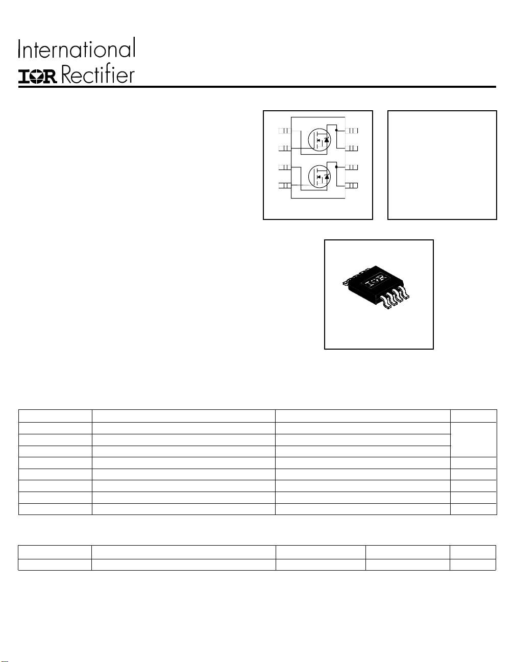
S1
G1
S2
G2
1
2
3
4
To p V iew
PD - 9.1266G
IRF7503
HEXFET® Power MOSFET
8
D1
V
7
D1
6
D2
5
D2
R
DS(on)
= 30V
DSS
= 0.135Ω
The new Micro8 package, with half the footprint area of the
standard SO-8, provides the smallest footprint available in
Micro8
an SOIC outline. This makes the Micro8 an ideal device for
applications where printed circuit board space is at a
premium. The low profile (<1.1mm) of the Micro8 will allow
it to fit easily into extremely thin application environments
such as portable electronics and PCMCIA cards.
Absolute Maximum Ratings
Parameter Max. Units
ID @ TA = 25°C Continuous Drain Current, VGS @ 10V 2.4
ID @ TA = 70°C Continuous Drain Current, VGS @ 10V 1.9 A
I
DM
PD @TA = 25°C Power Dissipation 1.25 W
V
GS
dv/dt Peak Diode Recovery dv/dt 5.0 V/ns
T
J, TSTG
Pulsed Drain Current 14
Linear Derating Factor 10 mW/°C
Gate-to-Source Voltage ± 20 V
Junction and Storage Temperature Range -55 to + 150 °C
Thermal Resistance
Parameter Typ. Max. Units
R
θJA
All Micro8 Data Sheets reflect improved Thermal Resistance, Power and Current -Handling Ratings- effective
only for product marked with Date Code 505 or later .
Maximum Junction-to-Ambient ––– 100
°C/W
8/25/97
Page 2
IRF7503
Electrical Characteristics @ TJ = 25°C (unless otherwise specified)
Parameter Min. Typ. Max. Units Conditions
V
(BR)DSS
∆V
(BR)DSS
R
DS(on)
V
GS(th)
g
fs
I
DSS
I
GSS
Gate-to-Source Reverse Leakage ––– ––– 100 VGS = 20V
Q
g
Q
gs
Q
gd
t
d(on)
t
r
t
d(off)
t
f
C
iss
C
oss
C
rss
Drain-to-Source Breakdown Voltage 30 ––– ––– V VGS = 0V, ID = 250µA
/∆T
Breakdown Voltage Temp. Coefficient ––– 0.059 ––– V/°C Reference to 25°C, ID = 1mA
J
Static Drain-to-Source On-Resistance
––– ––– 0.135 VGS = 10V, ID = 1.7A
––– ––– 0.222 VGS = 4.5V, ID = 0.85A
Ω
Gate Threshold Voltage 1.0 ––– ––– V VDS = VGS, ID = 250µA
Forward Transconductance 1.9 ––– ––– S VDS = 10V, ID = 0.85A
Drain-to-Source Leakage Current
Gate-to-Source Forward Leakage ––– ––– -100 VGS = -20V
––– ––– 1.0 VDS = 24V, VGS = 0V
––– ––– 25 VDS = 24V, VGS = 0V, TJ = 125°C
µA
nA
Total Gate Charge ––– 7.8 12 ID = 1.7A
Gate-to-Source Charge ––– 1.2 1.8 nC VDS = 24V
Gate-to-Drain ("Miller") Charge ––– 2.5 3.8 VGS = 10V, See Fig. 6 and 9
Turn-On Delay Time ––– 4.7 –– – VDD = 15V
Rise Time ––– 10 ––– ID = 1.7A
Turn-Off Delay Time ––– 12 ––– RG = 6.1Ω
ns
Fall Time ––– 5.3 ––– RD = 8.7Ω, See Fig. 10
Input Capacitance ––– 210 ––– VGS = 0V
Output Capacitance ––– 80 ––– pF VDS = 25V
Reverse Transfer Capacitance ––– 32 ––– ƒ = 1.0MHz, See Fig. 5
Source-Drain Ratings and Characteristics
Parameter Min. Typ. Max. Units Conditions
I
S
I
SM
V
SD
t
rr
Q
rr
Notes:
Repetitive rating; pulse width limited by
max. junction temperature. ( See fig. 11 )
I
SD
TJ ≤ 150°C
Continuous Source Current MOSFET symbol
(Body Diode) showing the
Pulsed Source Current integral reverse
(Body Diode) p-n junction diode.
––– ––– 1.25
––– ––– 14
Diode Forward Voltage ––– ––– 1.2 V TJ = 25°C, IS = 1.7A, VGS = 0V
Reverse Recovery Time ––– 40 60 ns TJ = 25°C, IF = 1.7A
Reverse RecoveryCharge ––– 48 7 2 nC di/dt = 100A/µs
Pulse width ≤ 300µs; duty cycle ≤ 2%.
≤ 1.7A, di/dt ≤ 120A/µs, V
DD
≤ V
(BR)DSS
,
Surface mounted on FR-4 board, t
D
A
≤ 10sec.
G
S
Page 3
IRF7503
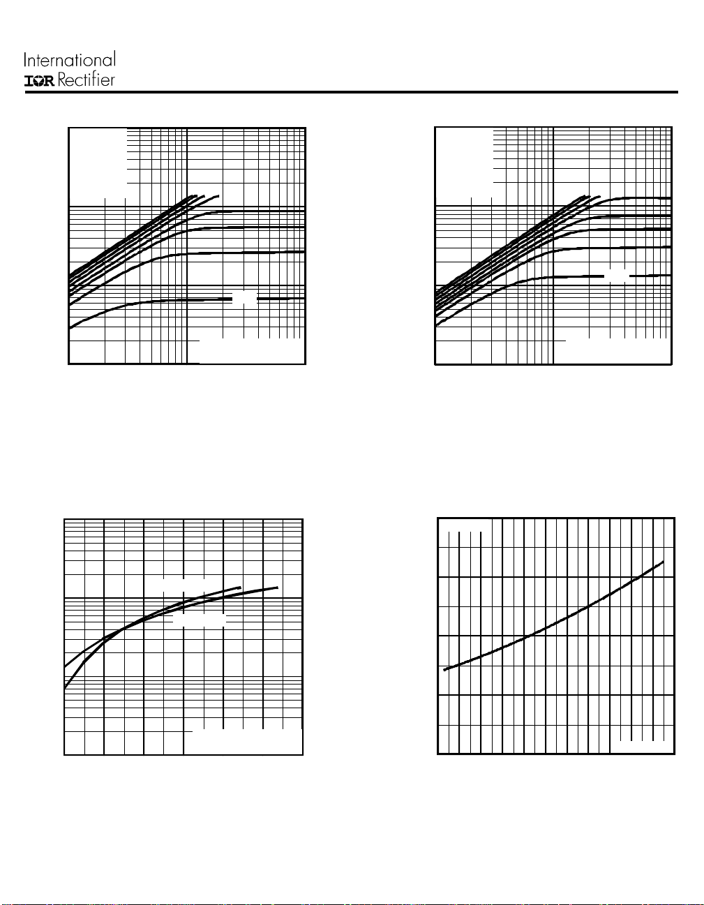
100
VGS
TOP 15V
10V
7.0V
5.5V
4.5V
4.0V
3.5V
BOTT OM 3.0V
10
1
3.0V
D
I , Drain-to-Source C urrent (A)
20µs PULSE WIDT H
T = 25 °C
0.1
0.1 1 10
V , Drain-to-Source Voltage (V)
DS
J
Fig 1. Typical Output Characteristics
100
100
VGS
TOP 15V
10V
7.0V
5.5V
4.5V
4.0V
3.5V
BOTT OM 3.0V
10
1
D
I , Drain-to-S ource C urrent (A)
3.0V
20µs PULSE WIDT H
T = 150°C
A
0.1
0.1 1 10
V , Drain-to -Sou rce Vo ltage ( V)
DS
J
A
Fig 2. Typical Output Characteristics
2.0
I = 1.7 A
D
T = 25°C
10
1
D
I , Dr a in-to - Sou r ce C u rr en t ( A)
0.1
3.0 3.5 4.0 4.5 5.0 5.5 6.0
V , Ga te-to-So urce Voltage (V)
GS
J
T = 150°C
J
V = 10V
DS
20µs PULSE W IDTH
Fig 3. Typical Transfer Characteristics
1.5
1.0
(No rm alized)
0.5
DS(on)
R , Dra in-to -S ourc e O n R e sista n ce
A
0.0
-60 -40 -20 0 20 40 60 80 100 120 140 160
T , Ju nc tio n T em perat u re ( °C )
J
V = 1 0V
GS
A
Fig 4. Normalized On-Resistance
Vs. Temperature
Page 4

IRF7503
400
300
200
C, C apac itance (pF)
100
0
1 10 100
V = 0V , f = 1 MH z
GS
C = C + C , C S HORTE D
iss gs gd ds
C = C
rss gd
C = C + C
oss ds gd
C
iss
C
oss
C
rs s
V , Drai n-to -Sourc e Voltage ( V)
DS
Fig 5. Typical Capacitance Vs.
Drain-to-Source Voltage
100
20
I = 1.7A
V , Gate- to -S ou rce V oltag e (V)
16
12
8
4
GS
D
V = 2 4V
DS
V = 1 5V
DS
FOR TEST CIRCUIT
A
0
024681012
Q , Total Ga te Ch arg e (nC)
G
SEE FIGURE 9
A
Fig 6. Typical Gate Charge Vs.
Gate-to-Source Voltage
100
O PER AT ION IN T HIS AREA LIMI TED
BY R
DS(on)
10
T = 150°C
J
T = 25°C
1
SD
I , Rev ers e Dr ain C u rren t (A)
0.1
0.4 0.8 1.2 1.6 2.0
V , Source-to-Drain Voltage (V)
SD
J
V = 0V
GS
Fig 7. Typical Source-Drain Diode
Forward Voltage
10
1
D
I , Drain Cu rrent (A )
T = 25°C
A
T = 150°C
J
A
Single Pulse
0.1
1 10 100
V , Drain-to-So urc e Vo ltag e (V)
DS
10µs
100µs
1ms
10ms
A
Fig 8. Maximum Safe Operating Area
Page 5

+
-
10V
V
IRF7503
R
D.U.T.
D
V
DD
V
Q
G
Q
GS
Q
GD
R
DS
V
GS
G
G
10V
Pulse Width ≤ 1 µs
Charge
Duty Factor ≤ 0.1 %
Fig 9a. Basic Gate Charge Waveform
Current Regulator
Same Type as D.U.T.
50KΩ
.2µF
12V
.3µF
D.U.T .
+
V
DS
-
Fig 10a. Switching Time Test Circuit
V
DS
90%
10%
V
GS
3mA
I
G
Current Sampling Resistors
I
D
Fig 9b. Gate Charge Test Circuit
1000
100
thJA
D = 0.50
0.20
0.10
10
0.05
0.02
0.01
1
Thermal Response (Z )
0.1
0.00001 0.0001 0.001 0.01 0.1 1 10 100
SINGLE PULSE
(THERMAL RESPONSE)
t , Rectangular Pulse Duration (sec)
1
V
GS
t
d(on)tr
t
d(off)tf
Fig 10b. Switching Time Waveforms
P
DM
t
1
t
2
Notes:
1. Duty factor D = t / t
2. Peak T = P x Z + T
1 2
J DM thJA A
Fig 11. Maximum Effective Transient Thermal Impedance, Junction-to-Ambient
Page 6

IRF7503
+
-
Peak Diode Recovery dv/dt Test Circuit
+
D.U.T
-
R
G
Driver Gate Drive
P.W.
+
Circuit Layout Considerations
• Low Stray Inductance
• Ground Plane
• Low Leakage Inductance
Current Transformer
-
• dv/dt controlled by R
• Driver same type as D.U.T.
controlled by Duty Factor "D"
• I
SD
• D.U.T. - Device Under Test
Period
-
D =
G
Period
P.W.
+
V
DD
VGS=10V
*
Reverse
Recovery
Current
Re-Applied
Voltage
D.U.T. ISDWaveform
Body Diode Forward
D.U.T. VDSWaveform
Body Diode Forward Drop
Inductor Curent
Ripple ≤ 5%
* V
= 5V for Logic Level Devices
GS
Fig 12. For N-Channel HEXFETS
Current
di/dt
Diode Recovery
dv/dt
V
DD
I
SD
Page 7

Package Outline
Micro8 Outline
Dimensions are shown in millimeters (inches)
IRF7503
D
3
- B -
3
- A -
- C B 8X
NOTES:
1 DIM E N SIONING AND TO LER AN C ING PER AN SI Y14.5M-1982.
2 CONTROLLING DIMENSION : INCH.
3 DIME N S IO NS DO NO T INCL UDE MO LD F L A S H.
8 7 6 5
E
0.25 (.010) M A M
1 2 3 4
e
6X
e 1
A
A 1
0.08 ( .0 0 3) M C A S B S
Part Marking Information
Micro8
H
0. 10 (.00 4)
LEAD ASSIGNM ENTS
D D D D D1 D1 D2 D2
8 7 6 5 8 7 6 5
SINGLE
1 2 3 4
S S S G
θ
L
8X
DUAL
1 2 3 4
S1 G1 S2 G2
8X
IN C H E S M IL L IM E T E R S
DIM
M IN M AX M IN M AX
A .036 .044 0.91 1.11
A1 .004 .008 0.10 0.20
B .010 .014 0.25 0.36
C .005 .007 0.13 0.18
D .116 .120 2.95 3.05
e .0256 BASIC 0.65 BASIC
e1 .0128 BASIC 0.33 BA SIC
E .116 .120 2.95 3.05
H .188 .198 4.78 5.03
L .016 .026 0.41 0.66
θ
0 ° 6 ° 0° 6 °
RECOMMENDED FOOTPRINT
1.04
( .041 )
C
8 X
3.20
( .126 )
0.38
( .015 )
4. 2 4
( .167 )
0 . 6 5
( .0256 )
6X
8X
5.28
( .208 )
EX AMP LE : T HIS IS A N IRF7501
PART NUM BER
451
7501
TOP
DATE CODE (YW W)
A
Y = LA ST D IG IT O F YE A R
W W = WEEK
Page 8

IRF7503
Tape & Reel Information
Micro8
Dimensions are shown in millimeters (inches)
TERMINAL NUMBER 1
12.3 ( .484 )
11.7 ( .461 )
8.1 ( .318 )
7.9 ( .312 )
NOTES:
1. O U TL INE CO N FORM S TO EIA-481 & EIA-541.
2. CONTRO LLING DIMENSION : MILLIME TER.
330.00
(12.992)
MAX.
NOTES :
1. CONTROLLING DIMENSION : MILLIMETER.
2. OUTLINE CONFORMS TO EIA-481 & EIA-541.
FEED DIRECTION
14.40 ( .566 )
12.40 ( .488 )
WORLD HEADQUARTERS: 233 Kansas St., El Segundo, California 90245, Tel: (310) 322 3331
EUROPEAN HEADQUARTERS: Hurst Green, Oxted, Surrey RH8 9BB, UK Tel: ++ 44 1883 732020
IR CANADA: 7321 Victoria Park Ave., Suite 201, Markham, Ontario L3R 2Z8, Tel: (905) 475 1897
IR GERMANY: Saalburgstrasse 157, 61350 Bad Homburg Tel: ++ 49 6172 96590
IR ITALY: Via Liguria 49, 10071 Borgaro, Torino Tel: ++ 39 11 451 0111
IR FAR EAST: K&H Bldg., 2F, 30-4 Nishi-Ikebukuro 3-Chome, Toshima-Ku, Tokyo Japan 171 Tel: 81 3 3983 0086
IR SOUTHEAST ASIA: 315 Outram Road, #10-02 Tan Boon Liat Building, Singapore 0316 Tel: 65 221 8371
http://www.irf.com/ Data and specifications subject to change without notice. 8/97
 Loading...