

Page 1
SMPS MOSFET
A
PD-93896
IRF7465
HEXFET® Power MOSFET
Applications
l High frequency DC-DC converters
V
DSS
150V 0.28
R
DS(on)
ΩΩ
Ω@V
ΩΩ
max I
= 10V 1.9A
GS
D
Benefits
l Low Gate to Drain Charge to Reduce
Switching Losses
l Fully Characterized Capacitance Including
Effective C
to Simplify Design (See
OSS
App. Note AN1001)
l Fully Characterized Avalanche Voltage
and Current
S
S
S
1
2
3
4
Top V iew
A
8
D
7
D
6
D
5
DG
SO-8
Absolute Maximum Ratings
Parameter Max. Units
ID @ TA = 25°C Continuous Drain Current, VGS @ 10V 1.9
ID @ TA = 70°C Continuous Drain Current, VGS @ 10V 1.5 A
I
DM
PD @TA = 25°C Power Dissipation 2.5 W
V
GS
dv/dt Peak Diode Recovery dv/dt 7.8 V/ns
T
J
T
STG
Pulsed Drain Current 15
Linear Derating Factor 0.02 W/°C
Gate-to-Source Voltage ± 30 V
Operating Junction and -55 to + 150
Storage Temperature Range
Soldering Temperature, for 10 seconds 300 (1.6mm from case )
°C
Thermal Resistance
Symbol Parameter Typ. Max. Units
R
θJL
R
θJA
Junction-to-Drain Lead ––– 20
Junction-to-Ambient ––– 50 °C/W
Notes through are on page 8
www.irf.com 1
2/8/01
Page 2
IRF7465
Static @ TJ = 25°C (unless otherwise specified)
Parameter Min. Typ. Max. Units Conditions
V
(BR)DSS
∆V
(BR)DSS
R
DS(on)
V
GS(th)
I
DSS
I
GSS
Dynamic @ TJ = 25°C (unless otherwise specified)
g
fs
Q
g
Q
gs
Q
gd
t
d(on)
t
r
t
d(off)
t
f
C
iss
C
oss
C
rss
C
oss
C
oss
C
eff. Effective Output Capacitance ––– 76 ––– VGS = 0V, VDS = 0V to 120V
oss
Drain-to-Source Breakdown Voltage 150 ––– ––– VVGS = 0V, ID = 250µA
/∆T
Breakdown Voltage Temp. Coefficient
J
––– 0.19 ––– V/°C Reference to 25°C, ID = 1mA
Static Drain-to-Source On-Resistance ––– ––– 0.28 Ω VGS = 10V, ID = 1.14A
Gate Threshold Voltage 3.0 ––– 5.5 V VDS = VGS, ID = 250µA
Drain-to-Source Leakage Current
––– ––– 25
––– ––– 250 VDS = 120V, VGS = 0V, TJ = 125°C
Gate-to-Source Forward Leakage ––– ––– 100 V
Gate-to-Source Reverse Leakage ––– ––– -100
VDS = 150V, VGS = 0V
µA
= 30V
GS
nA
V
= -30V
GS
Parameter Min. Typ. Max. Units Conditions
Forward Transconductance 0.75 ––– ––– SVDS = 50V, ID = 1.14A
Total Gate Charge ––– 10 15 ID = 1.14A
Gate-to-Source Charge ––– 2.7 4.0 nC VDS = 120V
Gate-to-Drain ("Miller") Charge ––– 5.0 7.5 VGS = 10V
Turn-On Delay Time ––– 7.0 ––– VDD = 75V
Rise Time ––– 1.2 ––– ID = 1.14A
Turn-Off Delay Time ––– 10 ––– RG = 6.0Ω
ns
Fall Time ––– 9.0 ––– VGS = 10V
Input Capacitance ––– 330 ––– VGS = 0V
Output Capacitance ––– 80 ––– VDS = 25V
Reverse Transfer Capacitance ––– 16 ––– pF ƒ = 1.0MHz
Output Capacitance ––– 420 ––– VGS = 0V, VDS = 1.0V, ƒ = 1.0MHz
Output Capacitance ––– 41 ––– VGS = 0V, VDS = 120V, ƒ = 1.0MHz
Avalanche Characteristics
Parameter Typ. Max. Units
E
AS
I
AR
Single Pulse Avalanche Energy ––– 40 mJ
Avalanche Current ––– 1.9 A
Diode Characteristics
Parameter Min. Typ. Max. Units Conditions
I
S
I
SM
V
SD
t
rr
Q
rr
Continuous Source Current MOSFET symbol
(Body Diode)
Pulsed Source Current integral reverse
(Body Diode)
––– –––
––– –––
2.3
15
showing the
A
p-n junction diode.
G
Diode Forward Voltage ––– ––– 1.3 V TJ = 25°C, IS = 1.14A, VGS = 0V
Reverse Recovery Time ––– 62 93 ns TJ = 25°C, IF = 1.14A
Reverse RecoveryCharge ––– 160 240 nC di/dt = 100A/µs
2 www.irf.com
D
S
Page 3
IRF7465
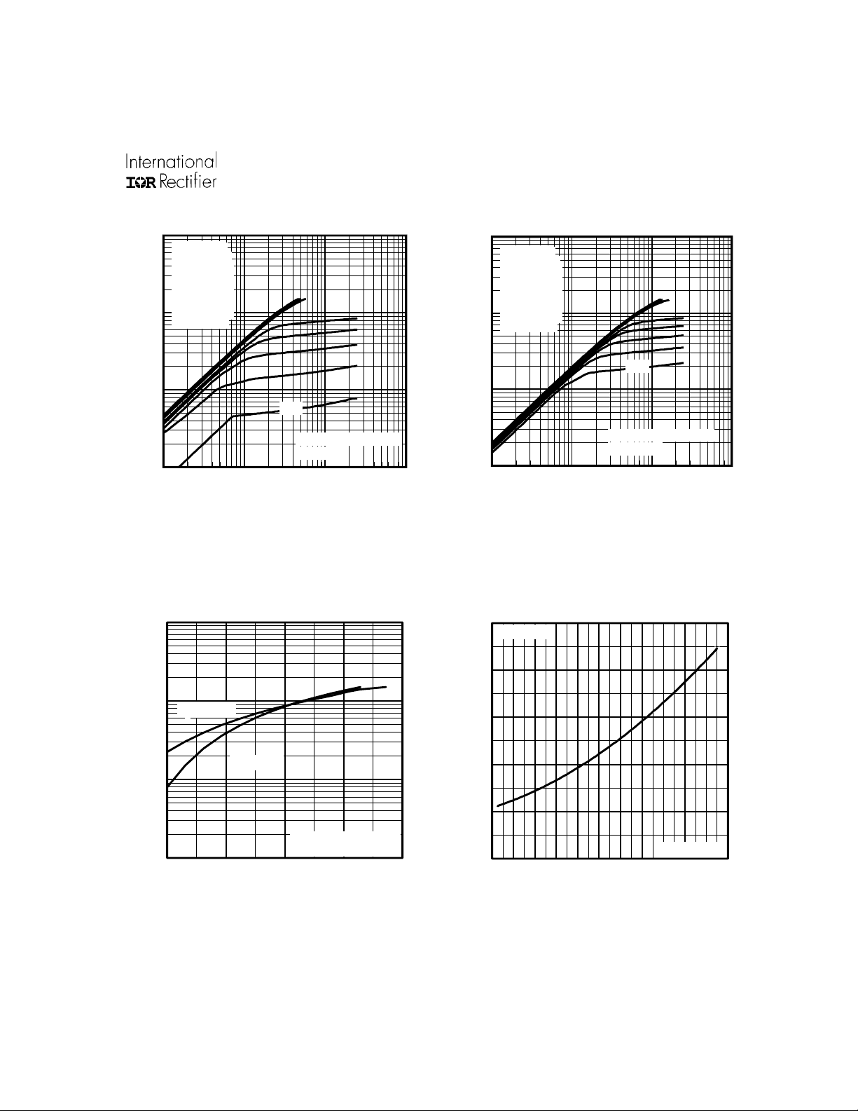
100
10
1
, Drain-to-Source Current (A)
D
I
VGS
TOP 15V
12V
10V
8.0V
7.5V
7.0V
6.5V
BOTTOM 6.0V
6.0V
20µs PULSE WIDTH
Tj = 25°C
0.1
0.1 1 10 100
VDS, Drain-to-Source Voltage (V)
Fig 1. Typical Output Characteristics
100
100
10
VGS
TOP 15V
12V
10V
8.0V
7.5V
7.0V
6.5V
BOTTOM 6.0V
6.0V
1
, Drain-to-Source Current (A)
D
I
20µs PULSE WIDTH
Tj = 150°C
0.1
0.1 1 10 100
VDS, Drain-to-Source Voltage (V)
Fig 2. Typical Output Characteristics
2.5
1.9A
I =
D
2.0
10
1
D
I , Drain-to-Source Current (A)
0.1
6.0 7.0 8.0 9.0 10.0
Fig 3. Typical Transfer Characteristics
°
T = 150 C
J
°
T = 25 C
J
V = 25V
DS
20µs PULSE WIDTH
V , Gate-to-Source Voltage (V)
GS
1.5
1.0
(Normalized)
0.5
DS(on)
R , Drain-to-Source On Resistance
0.0
-60 -40 -20 0 20 40 60 80 100 120 140 160
T , Junction Temperature ( C)
J
Fig 4. Normalized On-Resistance
V =
10V
GS
°
Vs. Temperature
www.irf.com 3
Page 4

IRF7465
10000
1000
V
= 0V, f = 1 MHZ
GS
C
= C
iss
gs
C
= C
rss
gd
C
= C
ds
+ C
oss
+ Cgd, C
gd
ds
Ciss
100
Coss
Crss
C, Capacitance(pF)
10
1
1 10 100 1000
VDS, Drain-to-Source Voltage (V)
Fig 5. Typical Capacitance Vs.
Drain-to-Source Voltage
100
SHORTED
20
I =
1.14A
D
V = 120V
DS
G
V = 75V
DS
V = 30V
DS
16
12
8
4
GS
V , Gate-to-Source Voltage (V)
0
0 4 8 12 16
Q , Total Gate Charge (nC)
Fig 6. Typical Gate Charge Vs.
Gate-to-Source Voltage
100
OPERATION IN THIS AREA
LIMITED BY RDS(on)
10
°
T = 150 C
J
°
T = 25 C
1
J
10
100µsec
1
1msec
SD
I , Reverse Drain Current (A)
V = 0 V
0.1
0.4 0.6 0.8 1.0
V ,Source-to-Drain Voltage (V)
SD
GS
Fig 7. Typical Source-Drain Diode
, Drain-to-Source Current (A)
TA = 25°C
D
I
TJ = 150°C
Single Pulse
0.1
1 10 100 1000
V
, Drain-toSource Voltage (V)
DS
Fig 8. Maximum Safe Operating Area
10msec
Forward Voltage
4 www.irf.com
Page 5

IRF7465
(
)
2.0
1.5
1.0
D
I , Drain Current (A)
0.5
0.0
25 50 75 100 125 150
T , Case Temperature ( C)
C
°
Fig 9. Maximum Drain Current Vs.
Ambient Temperature
100
R
V
DS
V
GS
R
G
10V
Pulse Width ≤ 1 µs
Duty Factor ≤ 0.1 %
D
D.U.T.
Fig 10a. Switching Time Test Circuit
V
DS
90%
10%
V
GS
t
d(on)tr
t
d(off)tf
Fig 10b. Switching Time Waveforms
+
V
DD
-
D = 0.50
thJA
0.20
10
0.10
0.05
P
0.02
1
0.01
Thermal Response (Z )
0.1
0.00001 0.0001 0.001 0.01 0.1 1 10
SINGLE PULSE
THERMAL RESPONSE
Notes:
1. Duty factor D = t / t
2. Peak T = P x Z + T
t , Rectangular Pulse Duration (sec)
1
J DM thJA A
DM
t
1
1 2
t
2
Fig 11. Maximum Effective Transient Thermal Impedance, Junction-to-Ambient
www.irf.com 5
Page 6

IRF7465
(BR)
A
)
0.40
Ω
0.36
0.32
V
= 10V
GS
0.28
0.24
( on) , Drain-to-Source On Resistance (
DS
0.20
R
0 4 8 12 16
ID , Drain Current (A)
Fig 12. On-Resistance Vs. Drain Current
Current Regulator
Same Type as D.U.T.
.2µF
12V
V
GS
50KΩ
.3µF
D.U.T.
3mA
I
G
Current Sampling Resistors
V
GS
+
V
DS
-
I
D
V
G
QGSQ
Q
G
GD
Charge
)
0.50
Ω
0.45
0.40
0.35
0.30
, Drain-to -Source On Resistance (
0.25
DS(on)
R
0.20
ID = 1.14A
6 8 10 12 14 16
V
Gate -to -Source Voltage (V)
GS,
Fig 13. On-Resistance Vs. Gate Voltage
100
TOP
80
BOTTOM
I
D
0.8A
1.5A
1.9A
Fig 14a&b. Basic Gate Charge Test Circuit
60
and Waveform
40
15V
V
t
p
I
AS
DSS
V
R
G
20V
L
DS
D.U.T
I
AS
Ω
0.01
t
p
Fig 15a&b. Unclamped Inductive Test circuit
and Waveforms
DRIVER
+
V
DD
-
20
AS
E , Single Pulse Avalanche Energy (mJ)
0
25 50 75 100 125 150
Starting T , Junction Temperature ( C)
J
Fig 15c. Maximum Avalanche Energy
Vs. Drain Current
°
6 www.irf.com
Page 7

SO-8 Package Details
D
5
- B -
8 7 6 5
5
E
- A 1 2 3 4
e
6X
- C -
0.25 ( .0 1 0 ) M C A S B S
NOTES:
1. DIMENSIONING AND TOLERANCING PER ANSI Y14.5M-1982.
2. C O NT RO L LIN G DIM ENS IO N : IN CH .
3. DIMENSIONS ARE SHOWN IN MILLIMETERS (INCHES).
4. O U T L IN E C ON FO R M S T O JE DEC OU T LIN E M S-01 2A A .
DIMENSION DOES NOT INCLUDE MOLD PROTRUSIONS
5
M O LD P R OT R U SION S N OT T O EXC E E D 0 .2 5 (.0 0 6).
DIM E N S IO NS IS TH E LE N GT H O F LE A D F OR S OLD E R IN G T O A S U B S TR ATE ..
6
B 8X
e1
A1
H
0 .2 5 (.0 1 0) M A M
A
0.10 (.004)
θ
θ
L
8X
K x 45°
6
C
8X
IRF7465
IN CH E S M IL L IME TERS
DIM
M IN MAX M IN MAX
A .0 532 .0 688 1 .35 1 .7 5
A1 .0 040 .0 098 0 .10 0 .2 5
B .0 14 .0 18 0 .36 0 .4 6
C .0 075 .0 0 9 8 0 .1 9 0.2 5
D .1 89 .1 9 6 4 .8 0 4.9 8
E .1 50 .1 57 3 .81 3 .9 9
e .0 5 0 BASIC 1 .2 7 BASIC
e1 .0 2 5 BASIC 0.635 BASIC
H .2 284 .2 4 4 0 5 .80 6 .2 0
K .0 11 .0 19 0 .28 0 .4 8
L 0 .1 6 .0 50 0 .41 1 .2 7
θ
0 ° 8 ° 0 ° 8 °
RECOMMENDED FOOTPRINT
0.72 (.028 )
8X
6.46 ( .255 )
1.27 ( .050 )
3X
1.78 (.070)
8X
SO-8 Part Marking
www.irf.com 7
Page 8

IRF7465
(
)
)
)
)
)
)
)
(
SO-8 Tape and Reel
TERMINAL NUMBER 1
12.3 ( .484
11.7 ( .461
8.1 ( .318
7.9 ( .312
NOTES:
1. CONTROLLING DIMENSION : MILLIMETER .
2. ALL DIMENSIONS ARE SHOW N IN MILLIMETERS
3. OUTLINE CONFORM S TO EIA-481 & EIA-541.
NOT ES :
1. CONTRO LL ING DIMEN SION : MILLIMETER.
2. OUTLINE CO NF O RM S TO EIA-481 & EIA-541.
Notes:
Repetitive rating; pulse width limited by
max. junction temperature.
Starting T
RG = 25Ω, I
= 25°C, L = 22mH
J
= 1.9A.
AS
FEED DIRECTION
INC HE S).
330.00
12.992
MAX.
14.40 ( .566
12.40 ( .488
Pulse width ≤ 400µs; duty cycle ≤ 2%.
When mounted on 1 inch square copper board
Data and specifications subject to change without notice.
This product has been designed and qualified for the industrial market.
Qualification Standards can be found on IR’s Web site.
IR WORLD HEADQUARTERS: 233 Kansas St., El Segundo, California 90245, USA Tel: (310) 252-7105
TAC Fax: (310) 252-7903
Visit us at www.irf.com for sales contact information. 2/01
8 www.irf.com
 Loading...