

Page 1

PD -91703A
1
1
2
2
G
S
G
IRF7341
l Generation V Technology
l Ultra Low On-Resistance
l Dual N-Channel Mosfet
l Surface Mount
l Available in Tape & Reel
l Dynamic dv/dt Rating
l Fast Switching
Description
Fifth Generation HEXFETs from International Rectifier
utilize advanced processing techniques to achieve
extremely low on-resistance per silicon area. This
benefit, combined with the fast switching speed and
ruggedized device design that HEXFET Power
MOSFETs are well known for, provides the designer
with an extremely efficient and reliable device for use
in a wide variety of applications.
The SO-8 has been modified through a customized
leadframe for enhanced thermal characteristics and
multiple-die capability making it ideal in a variety of
power applications. With these improvements, multiple
devices can be used in an application with dramatically
reduced board space. The package is designed for
vapor phase, infra red, or wave soldering techniques.
Power dissipation of greater than 0.8W is possible in
a typical PCB mount application.
S1
1
2
2
1
2
3
4
Top View
HEXFET® Power MOSFET
8
D
V
7
D
6
D
5
D
R
DS(on)
SO-8
= 55V
DSS
= 0.050Ω
Absolute Maximum Ratings
Parameter Max. Units
V
DS
ID @ TC = 25°C Continuous Drain Current, VGS @ 10V 4.7
ID @ TC = 70°C Continuous Drain Current, VGS @ 10V 3.8 A
I
DM
PD @TC = 25°C Power Dissipation 2.0
PD @TC = 70°C Power Dissipation 1.3
V
GS
V
GSM
E
AS
dv/dt Peak Diode Recovery dv/dt 5.0 V/ns
T
J, TSTG
Drain- Source Voltage 55 V
Pulsed Drain Current 38
W
Linear Derating Factor 0.016 W/°C
Gate-to-Source Voltage ± 20 V
Gate-to-Source Voltage Single Pulse tp<10µs 30 V
Single Pulse Avalanche Energy 72
Junction and Storage Temperature Range -55 to + 150 °C
Thermal Resistance
Parameter Typ. Max. Units
R
θJA
Maximum Junction-to-Ambient ––– 62.5 °C/W
www.irf.com 1
4/11/05
Page 2

IRF7341
S
D
G
Electrical Characteristics @ TJ = 25°C (unless otherwise specified)
Parameter Min. Typ. Max. Units Conditions
V
(BR)DSS
∆V
(BR)DSS
R
DS(on)
V
GS(th)
g
fs
I
DSS
I
GSS
Q
g
Q
gs
Q
gd
t
d(on)
t
r
t
d(off)
t
f
C
iss
C
oss
C
rss
Drain-to-Source Breakdown Voltage 55 ––– ––– V VGS = 0V, ID = 250µA
/∆T
Breakdown Voltage Temp. Coefficient ––– 0.059 ––– V/°C Reference to 25°C, ID = 1mA
J
Static Drain-to-Source On-Resistance
––– 0.043 0.050 V
––– 0.056 0.065 VGS = 4.5V, ID = 3.8A
Ω
= 10V, ID = 4.7A
GS
Gate Threshold Voltage 1.0 –– – ––– V VDS = VGS, ID = 250µA
Forward Transconductance 7.9 ––– ––– S VDS = 10V, ID = 4.5A
Drain-to-Source Leakage Current
Gate-to-Source Forward Leakage ––– ––– -100 VGS = -20V
Gate-to-Source Reverse Leakage ––– – –– 100 VGS = 20V
––– ––– 2.0 VDS = 55V, VGS = 0V
––– ––– 25 VDS = 55V, VGS = 0V, TJ = 55°C
µA
nA
Total Gate Charge ––– 24 36 ID = 4.5A
Gate-to-Source Charge ––– 2.3 3.4 nC VDS = 44V
Gate-to-Drain ("Miller") Charge ––– 7.0 10 VGS = 10V, See Fig. 10
Turn-On Delay Time ––– 8.3 12 VDD = 28V
Rise Time ––– 3.2 4.8 ID = 1.0A
Turn-Off Delay Time ––– 32 48 RG = 6.0Ω
ns
Fall Time ––– 13 20 RD = 28Ω,
Input Capacitance ––– 740 ––– VGS = 0V
Output Capacitance ––– 190 ––– pF VDS = 25V
Reverse Transfer Capacitance ––– 71 ––– ƒ = 1.0MHz, See Fig. 9
Source-Drain Ratings and Characteristics
Parameter Min. Typ. Max. Units Conditions
I
S
I
SM
V
SD
t
rr
Q
rr
Continuous Source Current MOSFET symbol
(Body Diode) showing the
Pulsed Source Current integral reverse
(Body Diode) p-n junction diode.
2.0
A
38
Diode Forward Voltage ––– ––– 1.2 V TJ = 25°C, IS = 2.0A, VGS = 0V
Reverse Recovery Time ––– 60 90 n s TJ = 25°C, IF = 2.0A
Reverse RecoveryCharge ––– 120 170 nC di/dt = -100A/µs
Notes:
Repetitive rating; pulse width limited by
max. junction temperature. ( See fig. 11 )
Starting T
RG = 25Ω, I
= 25°C, L = 6.5mH
J
= 4.7A. (See Figure 8)
AS
I
≤ 4.7A, di/dt ≤ 220A/µs, V
SD
DD
≤ V
TJ ≤ 150°C
Pulse width ≤ 300µs; duty cycle ≤ 2%.
(BR)DSS
,
When mounted on 1 inch square copper board, t<10 sec
2 www.irf.com
Page 3
IRF7341
100
10
TOP
BOTTOM
VGS
15V
12V
10V
8.0V
6.0V
4.5V
4.0V
3.5V
3.0V
3.0V
D
I , Drain-to-Source Current (A)
20µs PULSE WIDTH
°
T = 25 C
1
0.1 1 10 100
V , Drain-to-Sou rce Voltage (V)
DS
J
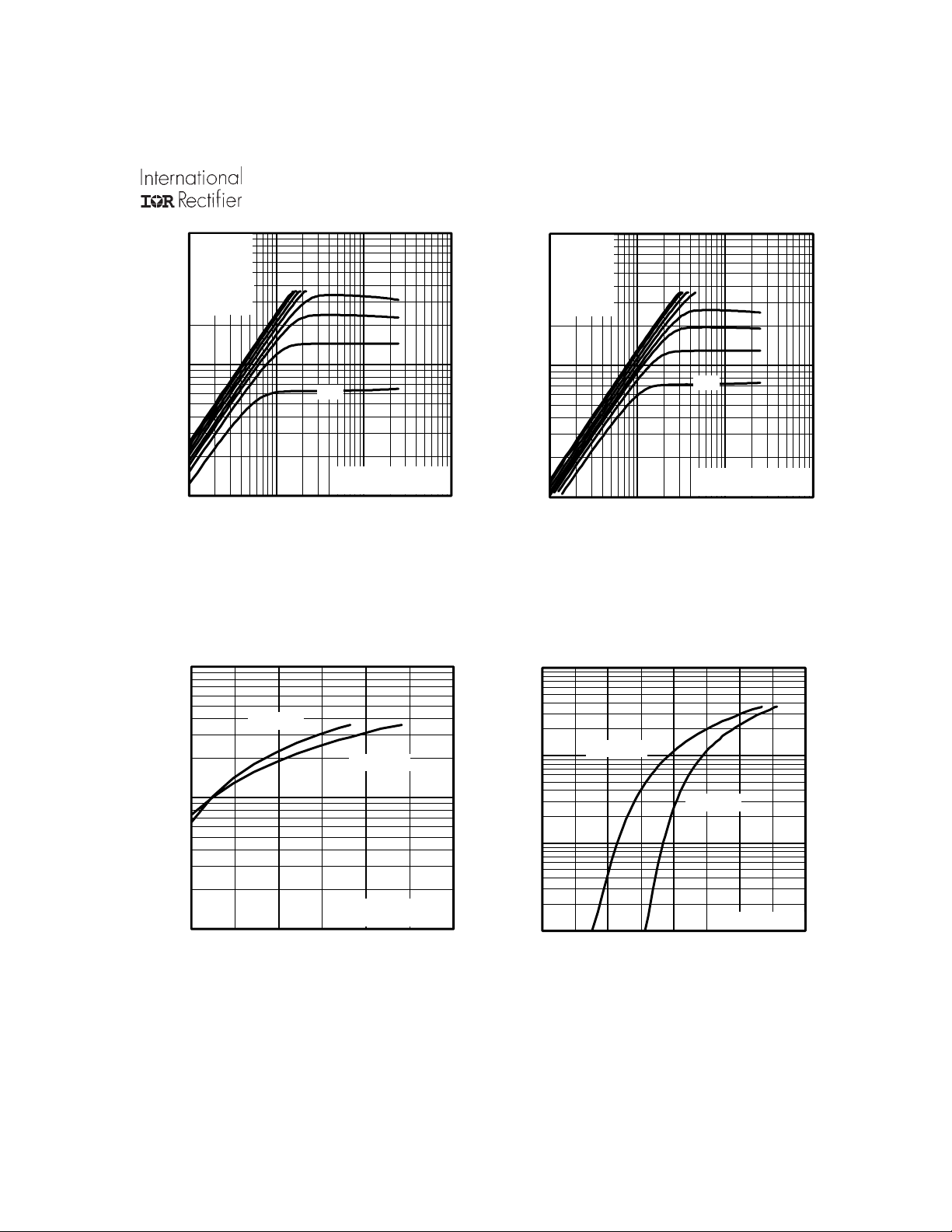
Fig 1. Typical Output Characteristics
100
100
10
TOP
BOTTOM
VGS
15V
12V
10V
8.0V
6.0V
4.5V
4.0V
3.5V
3.0V
3.0V
D
I , Drain-to-Source Current (A)
20µs PULSE WIDTH
1
0.1 1 10 100
V , Drain-to-Source Voltage (V)
DS
T = 150 C
°
J
Fig 2. Typical Output Characteristics
100
°
T = 25 C
J
°
T = 150 C
T = 150 C
J
10
D
I , Drain-to-Source Current (A)
V = 25V
DS
1
3 4 5 6
V , Gate-to-Source Voltage (V)
GS
20µs PULSE WIDTH
Fig 3. Typical Transfer Characteristics
°
10
1
SD
I , Reverse Drain Current (A)
0.1
0.2 0.5 0.8 1.1 1.4
Fig 4. Typical Source-Drain Diode
J
°
T = 25 C
J
V = 0 V
GS
V ,Source-to-Drain Voltage (V)
SD
Forward Voltage
www.irf.com 3
Page 4

IRF7341
0
0
0
0
0
A
2.5
2.0
1.5
1.0
(Normalized)
0.5
DS(on)
R , Drain-to-Source On Resistance
0.0
4.7A
I =
D
V =
10V
GS
-60 -40 -20 0 20 40 60 80 100 120 140 160
T , Junction Temperature ( C)
J
°
Fig 5. Normalized On-Resistance
Vs. Temperature
.12
( Ω )
e
c
n
ta
.10
is
s
e
R
n
O
e
.08
rc
u
o
-S
-to
in
ra
.06
, D
DS(on)
R
.04
0246810
V , Gate-to-Sourc e Vo ltage (V)
GS
I = 4.7A
D
0.120
(Ω)
0.100
0.080
VGS = 4.5V
0.060
VGS = 10V
DS (on)
0.040
R , Drain-to-Source On Resistance
0 10 20 30 40
I , Drain Current (A)
D
Fig 6. Typical On-Resistance Vs. Drain
Current
200
TOP
160
120
80
40
AS
E , Single Pulse Avalanche Energy (mJ)
0
25 50 75 100 125 150
Starting T , Junction Temperature ( C)
J
BOTTOM
I
D
2.1A
3.8A
4.7A
°
Fig 7. Typical On-Resistance Vs. Gate
Voltage
Fig 8. Maximum Avalanche Energy
Vs. Drain Current
4 www.irf.com
Page 5

IRF7341
1200
1000
800
600
400
C, Capacitance (pF)
200
0
1 10 100
V
=
0V,
GS
C
=
iss gs gd , ds
C
=
rss gd
C
=
oss ds gd
V , Drain-to-Source Voltage (V)
DS
f = 1MHz
C
+ C
C SHORTED
C
C
+ C
C
iss
C
oss
C
rss
Fig 9. Typical Capacitance Vs.
Drain-to-Source Voltage
100
20
I =
4.5A
D
V = 48V
DS
V = 30V
G
DS
V = 12V
DS
16
12
8
4
GS
V , Gate-to-Source Voltage (V)
0
0 10 20 30 40
Q , Total Gate Charge (nC)
Fig 10. Typical Gate Charge Vs.
Gate-to-Source Voltage
D = 0.50
thJA
Thermal Response (Z )
0.20
10
0.10
0.05
0.02
0.01
1
SINGLE PULSE
(THERMAL RESPONSE)
Notes:
1. Duty fa c to r D = t / t
2. Peak T = P x Z + T
0.1
0.0001 0.001 0.01 0.1 1 10 100
t , Rectangular Pulse Duration (sec)
1
J DM thJA A
1 2
P
DM
t
1
t
2
Fig 11. Maximum Effective Transient Thermal Impedance, Junction-to-Ambient
www.irf.com 5
Page 6

IRF7341
]
SO-8 Package Outline
Dimensions are shown in millimeters (inches)
D B
A
87
6
E
e
6X
5
65
4312
e1
0.25 [.010]
A
.0688
.0098
.020
.1968
.1574
.2440
.0196
.050
8°
MILLIMETERSINCHES
MIN MAX
1.35
1.75
0.10
0.25
0.33
0.51
4.80
5.00
3.80
4.00
1.27 BASIC
5.80
6.20
0.25
0.50
0.40
1.27
0°
8°
DIM
MIN MAX
.0532
A
.0040
A1
.013
b
H
A
C
y
c .0075 .0098 0.19 0.25
.189
D
.1497
E
.050 BASIC
e
e1
.025 BASIC 0.635 BASIC
.2284
H
.0099
K
.016
L
0°
y
K x 45°
0.25 [.010] C A B
NOTES:
1. DIMENSIONING & TOLERANCING PER ASME Y14.5M-1994.
2. CONTROLLING DIMENSION: MILLIMETER
3. DIMENS IONS ARE S HOWN IN MILL IMETERS [INCHE S].
4. OU TLI NE CONF ORMS TO JE DEC OU TLINE MS -012AA.
5 DIMENS ION DOES NOT INCLUDE MOLD PROTRUSIONS.
MOLD PROTRUS IONS NOT TO EXCEED 0.15 [.006].
6 DIMENS ION DOES NOT INCLUDE MOLD PROTRUSIONS.
MOLD PROTRUS IONS NOT TO EXCEED 0.25 [.010].
7 DIMENSION IS THE LENGTH OF LEAD FOR SOLDERING TO
A SUBST RATE.
SO-8 Part Marking
EXAMPLE: THIS IS AN IRF7101 (MOSFET)
INTERNATIONAL
RECTIFIER
LOGO
8X b
A1
0.10 [.004]
8X L
7
6.46 [.255]
3X 1.27 [.050]
8X c
FOOTPRINT
8X 0.72 [.028]
8X 1.78 [.070
DATE CODE (YWW)
P = DE S IGNAT E S L E AD-FREE
PRODUCT (O PTIONAL)
Y = LAST DI GIT OF THE YEAR
XXXX
F7101
WW = WEEK
A = ASSEMBLY SITE CODE
LOT COD E
PART NUMBER
6 www.irf.com
Page 7

TERMINAL NUMBER 1
N
1
2
3
SO-8 Tape and Reel
Dimensions are shown in millimeters (inches)
12.3 ( .484 )
11.7 ( .461 )
IRF7341
8.1 ( .318 )
7.9 ( .312 )
OTES:
. CONTROLLING DIMENSION : MILLIMETER.
. ALL DIMENSIONS ARE SHOWN IN MILLIMETERS(INCHES).
. OUTLINE CONFORMS TO EIA-481 & EIA-541.
330.00
(12.992)
MAX.
NOTES :
1. CONTROLLING DIMENSION : MILLIMETER.
2. OUTLINE CONFORMS TO EIA-481 & EIA-541.
Data and specifications subject to change without notice.
FEED DIRECTION
14.40 ( .566 )
12.40 ( .488 )
IR WORLD HEADQUARTERS: 233 Kansas St., El Segundo, California 90245, USA Tel: (310) 252-7105
TAC Fax: (310) 252-7903
Visit us at www.irf.com for sales contact information. 04/05
www.irf.com 7
 Loading...