

Page 1

IRF630S
N - CHANNEL 200V - 0.35Ω -9A-D2PAK
MESH OVERLAY MOSFET
TYPE V
DSS
R
DS(on)
I
D
IRF 630S 200 V < 0.40 Ω 9A
■ TYPICALR
■ EXTREMELY HIGH dv/dt CAPABILITY
■ 100%AVALANCHETESTED
■ VERYLOW INTRINSICCAPACITANCES
■ GATECHARGE MINIMIZED
■ FORTHROUGH-HOLE VERSION CONTACT
DS(on)
= 0.35 Ω
SALESOFFICE
DESCRIPTION
This power MOSFET is designed using the
company’sconsolidatedstrip layout-based MESH
OVERLAY process. This technology matches
and improves the performances compared with
standardpartsfrom various sources.
APPLICATIONS
■ HIGHCURRENT SWITCHING
■ UNINTERRUPTIBLE POWERSUPPLY(UPS)
■ DC/DC COVERTERSFOR TELECOM,
INDUSTRIAL,AND LIGHTING EQUIPMENT.
3
1
D2PAK
TO-263
(suffix ”T4”)
INTERNAL SCHEMATIC DIAGRAM
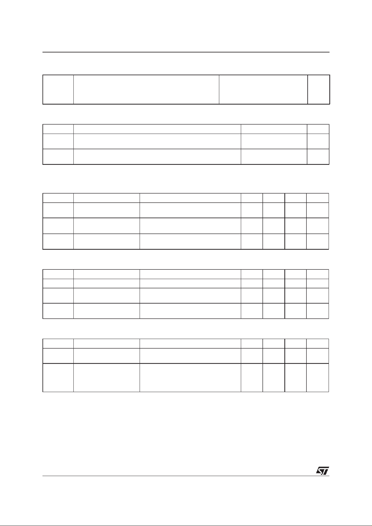
ABSOLUTE MAXIMUM RATINGS
Symbol Parameter Value Unit
V
V
V
I
DM
P
dv/dt(
T
(•) Pulse width limited by safe operating area (1)ISD≤ 9A, di/dt ≤ 300 A/µs,VDD≤ V
December 1998
Dra in- sour c e Vol t age (VGS= 0) 200 V
DS
Dra in- gate Volt age (RGS=20kΩ) 200 V
DGR
Gat e-source Voltage ± 20 V
GS
Dra in Current (c ont inuous) at Tc=25oC9A
I
D
Dra in Current (c ont inuous) at Tc=100oC5.7A
I
D
(•) Dra in Current (p ulsed) 36 A
Tot al Dissipation at Tc=25oC70W
tot
Der ati ng Factor 0.56 W/
1) Peak Di ode Recov ery voltage slope 5 V/ns
St orage Tem pe r ature -65 to 150
stg
Max. Operat ing J unction Temperature 150
T
j
,Tj≤T
(BR)DSS
JMAX
o
C
o
C
o
C
1/8
Page 2
IRF630S
THERMAL DATA
R
thj-case
Rthj-a mb
R
thc-sink
T
AVALANCHE CHARACTERISTICS
Symbol Parameter Max Value Unit
I
AR
E
Ther mal Resistanc e Junct ion-case Max
Ther mal Resistanc e Junct ion-ambient Max
Ther mal Resistanc e Case-sink Ty p
Maximum Lead T e m pe ra t ure For Soldering Purp ose
l
Avalanche Current, Repetitive or Not-Repetitive
(pulse width limited by T
Single Pulse Avalan c he Energy
AS
(starting T
=25oC, ID=IAR,VDD=50V)
j
max)
j
1.47
62.5
0.5
300
9A
100 mJ
o
C/W
oC/W
o
C/W
o
C
ELECTRICAL CHARACTERISTICS
=25oC unless otherwisespecified)
(T
case
OFF
Symbol Paramete r Test Con ditions Min. Typ. Max. Unit
V
(BR)DSS
Drain-source
ID=250µAVGS= 0 200 V
Break dow n Voltage
I
DSS
I
GSS
Zero Gate Voltage
Drain Current ( V
GS
Gat e- bod y Leakage
Current (V
DS
=0)
=0)
V
=MaxRating
DS
=MaxRating Tc=125oC
V
DS
V
=± 30 V
GS
1
50
100 nA
±
ON(∗)
Symbol Paramete r Test Con ditions Min. Typ. Max. Unit
V
GS(th)
R
DS(on)
Gate Threshold Voltage VDS=VGSID= 250 µA 234V
Sta t ic Drain-sour ce On
VGS=10V ID= 5 A 0.35 0.40
Resistance
I
D(on)
On State Drain Current VDS>I
D(on)xRDS(on)max
10 A
VGS=10V
DYNAMIC
Symbol Paramete r Test Con ditions Min. Typ. Max. Unit
g
(∗)Forward
fs
Tr ansc on duc tance
C
C
C
Input C apacitance
iss
Out put Capacitance
oss
Reverse Tr ansfer
rss
Capacit a nc e
VDS>I
D(on)xRDS(on)maxID
=5A 3 4 S
VDS=25V f=1MHz VGS= 0 540
90
35
700
120
50
µ
µA
Ω
pF
pF
pF
A
2/8
Page 3

IRF630S
ELECTRICAL CHARACTERISTICS
(continued)
SWITCHING ON
Symbol Paramete r Test Con ditions Min. Typ. Max. Unit
t
d(on)
t
r
Turn-on Time
Rise Time
VDD=100V ID= 4.5 A
R
=4.7
G
Ω
VGS=10V
10
15
14
20
(see test circuit, figure 3)
Q
Q
Q
Tot al G at e Charge
g
Gat e- Source Char g e
gs
Gate-Drain Charge
gd
VDD= 160 V ID=9A VGS=10V 31
7.5
9
45 nC
SWITCHING OFF
Symbol Paramete r Test Con ditions Min. Typ. Max. Unit
t
r(Voff)
t
t
Off-voltage Rise T im e
Fall Time
f
Cross-over Time
c
VDD=160V ID=9A
=4.7 Ω VGS=10V
R
G
(see test circuit, figure 5)
12
12
25
17
17
35
SOURCEDRAINDIODE
Symbol Paramete r Test Con ditions Min. Typ. Max. Unit
I
SD
I
SDM
V
SD
t
Q
I
RRM
(∗) Pulsed: Pulse duration = 300µs, duty cycle 1.5 %
(•) Pulse width limited by safe operating area
Source-drain Current
(•)
Source-drain Current
9
36
(pulsed)
(∗)ForwardOnVoltage ISD=9A VGS=0 1.5 V
Reverse Recover y
rr
Time
Reverse Recover y
rr
ISD=9A di/dt=100A/µs
=50V Tj= 150oC
V
DD
(see test circuit, figure 5)
170
0.95
Charge
Reverse Recover y
11
Current
ns
ns
nC
nC
ns
ns
ns
A
A
ns
µ
A
C
SafeOperating Area Thermal Impedance
3/8
Page 4

IRF630S
OutputCharacteristics
Transconductance
TransferCharacteristics
Static Drain-sourceOn Resistance
Gate Charge vs Gate-sourceVoltage
4/8
CapacitanceVariations
Page 5

IRF630S
NormalizedGate ThresholdVoltage vs
Temperature
Source-drainDiode Forward Characteristics
NormalizedOn Resistancevs Temperature
5/8
Page 6

IRF630S
Fig. 1:
UnclampedInductive Load Test Circuit
Fig. 3: Switching Times Test Circuits For
ResistiveLoad
Fig. 1:
UnclampedInductive Waveform
Fig. 4: Gate Charge test Circuit
Fig. 5:
Test CircuitFor InductiveLoad Switching
And Diode Recovery Times
6/8
Page 7

TO-263 (D2PAK) MECHANICAL DATA
IRF630S
DIM.
MIN. TYP. MAX. MIN. TYP. MAX.
A 4.3 4.6 0.169 0.181
A1 2.49 2.69 0.098 0.106
B 0.7 0.93 0.027 0.036
B2 1.25 1.4 0.049 0.055
C 0.45 0.6 0.017 0.023
C2 1.21 1.36 0.047 0.053
D 8.95 9.35 0.352 0.368
E 10 10.28 0.393 0.404
G 4.88 5.28 0.192 0.208
L 15 15.85 0.590 0.624
L2 1.27 1.4 0.050 0.055
L3 1.4 1.75 0.055 0.068
mm inch
E
A
C2
L2
D
L
L3
B2
B
A1
C
G
P011P6/C
7/8
Page 8

IRF630S
Information furnished is believed to be accurate and reliable. However, STMicroelectronics assumes no responsibility for the consequences
of use of such information nor for any infringement of patents or other rights of third parties which may result from its use. No license is
granted by implication or otherwise under any patent or patent rights of STMicroelectronics. Specification mentioned in this publication are
subject tochange without notice. This publication supersedes and replaces all information previously supplied. STMicroelectronics products
are not authorized for use as critical components inlife support devices or systems without express written approval ofSTMicroelectronics.
The ST logo is a trademarkof STMicroelectronics
1998 STMicroelectronics – Printed in Italy – All Rights Reserved
STMicroelectronics GROUP OF COMPANIES
Australia - Brazil - Canada -China -France - Germany - Italy - Japan - Korea - Malaysia - Malta - Mexico - Morocco - The Netherlands -
Singapore - Spain - Sweden - Switzerland - Taiwan - Thailand - United Kingdom - U.S.A.
http://www.st.com
.
8/8
 Loading...