

Page 1
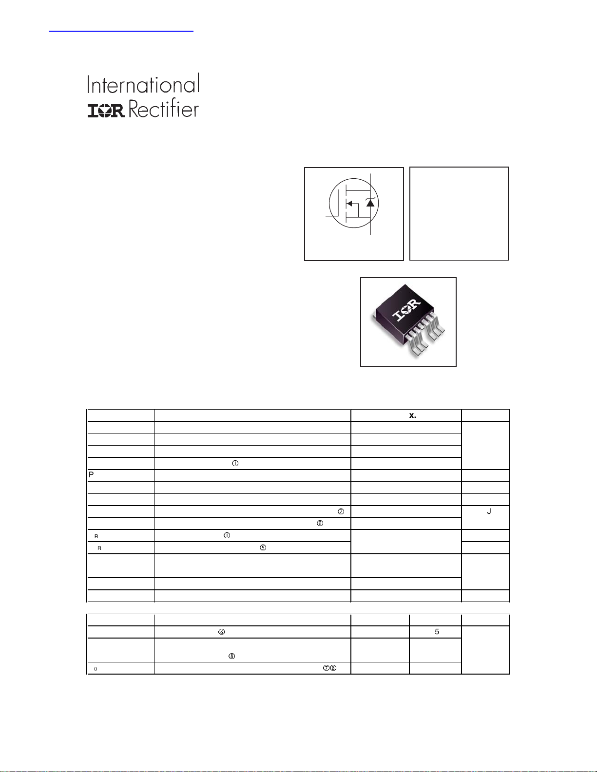
S
D
G
查询IRF2907ZS-7PPBF供应商
Features
l Advanced Process Technology
l Ultra Low On-Resistance
l 175°C Operating Temperature
l Fast Switching
l Repetitive Avalanche Allowed up to Tjmax
PD - 97031
IRF2907ZS-7PPbF
HEXFET® Power MOSFET
V
= 75V
DSS
R
DS(on)
= 3.8mΩ
Description
Specifically designed for high current, high reliability applications, this HEXFET® Power MOSFET
utilizes the latest processing techniques and advanced packaging technology to achieve extremely
low on-resistance and world -class current ratings.
Additional features of this design are a 175°C
junction operating temperature, fast switching speed
and improved repetitive avalanche rating . These
features combine to make this design an extremely
efficient and reliable device for use in Server &
Telecom OR'ing, Automotive and low voltage Motor
Drive Applications.
Absolute Maximum Ratings
Parameter Units
ID @ TC = 25°C
I
@ TC = 100°C
D
I
@ TC = 25°C
D
I
DM
PD @TC = 25°C
V
GS
E
AS
E
(tested)
AS
I
AR
E
AR
T
J
T
STG
Continuous Drain Current, V
Continuous Drain Current, V
Continuous Drain Current, V
Pulsed Drain Current
Maximum Power Dissipation
Linear Derating Factor
Gate-to-Source Voltage
Single Pulse Avalanche Energy (Thermally Limited)
Single Pulse Avalanche Energy Tested Value
Avalanche Current
Repetitive Avalanche Energy
Operating Junction and
Storage Temperature Range
Soldering Temperature, for 10 seconds
Mounting torque, 6-32 or M3 screw
c
c
@ 10V (Silicon Limited)
GS
@ 10V (See Fig. 9)
GS
@ 10V
GS
g
Thermal Resistance
Parameter Typ. Max. Units
R
θJC
R
θCS
R
θJA
R
θJA
Junct ion-to-Case
Case-to-Sink, Flat, Greased Surface
Junct ion-to-Ambient
Junct ion-to-Ambient (PCB Mount, steady state)
j
j
S (Pin 2, 3, 5, 6, 7)
G (Pin 1)
(Package Limited)
d
h
ij
ID = 160A
Max.
180
120
160
700
300
2.0
± 20
160
410
See Fig.12a,12b,15,16
-55 to + 175
300 (1.6mm from case )
10 lbf•in (1.1N•m)
––– 0.50 °C/W
0.50 –––
––– 62
––– 40
A
W
W/°C
V
mJ
A
mJ
°C
HEXFET® is a registered trademark of International Rectifier.
www.irf.com 1
08/03/05
Page 2
IRF2907ZS-7PPbF
/
g
µ
g
µ
Static @ TJ = 25°C (unless otherwise specified)
Parameter Min. Typ. Max. Units
V
(BR)DSS
∆Β
R
DS(on)
V
GS(th)
fs
I
DSS
I
GSS
Q
g
Q
gs
Q
gd
t
d(on)
t
r
t
d(off)
t
f
L
D
L
S
C
iss
C
oss
C
rss
C
oss
C
oss
C
oss
V
DSS
SMD
eff.
Drain-to-Source Breakdown Voltage75––––––V
∆
T
Breakdown Voltage Temp. Coefficient ––– 0.066 ––– V/°C
J
Static Drain-to-Source On-Resistance –––
3.0 3.8
Gate Threshold Voltage 2.0 ––– 4.0 V
Forward Transconductance
94 ––– ––– S
Drain-to-Source Leakage Current ––– ––– 20
––– ––– 250
Gate-to-Source Forward Leakage ––– ––– 200 nA
Gate-to-Source Reverse Leaka
e ––– ––– -200
Total Gate Charge ––– 170 260 nC
Gate-to-Source Charge ––– 55 –––
Gate-to-Drain ("Miller") Charge ––– 66 –––
Turn-On Delay Time ––– 21 ––– ns
Rise Time ––– 90 –––
Turn-Off Delay Time ––– 92 –––
Fall Time ––– 44 –––
Internal Drain Inductance ––– 4.5 ––– nH Between lead,
Internal Source Inductance ––– 7.5 ––– from package
Input Capacitance ––– 7580 ––– pF
Output Capacitance ––– 970 –––
Reverse Transfer Capacitance ––– 540 –––
Output Capacitance ––– 3750 –––
Output Capacitance ––– 650 –––
Effective Output Capacitance ––– 1110 –––
Conditions
VGS = 0V, ID = 250µA
Reference to 25°C, I
V
= 10V, ID = 110A
GS
mΩ
V
= VGS, ID = 250µA
DS
= 25V, ID = 110A
V
DS
V
A
= 75V, VGS = 0V
DS
V
= 75V, VGS = 0V, TJ = 125°C
DS
V
= 20V
GS
V
= -20V
GS
I
= 110A
D
V
= 60V
DS
e
= 10V
V
GS
= 38V
V
DD
= 110A
I
D
R
= 2.6Ω
G
V
GS
6mm (0.25in.)
and center of die contact
V
GS
V
DS
ƒ = 1.0MHz, See Fig. 5
V
GS
V
GS
VGS = 0V, VDS = 0V to 60V
d
= 10V
= 0V
= 25V
= 0V, VDS = 1.0V, ƒ = 1.0MHz
= 0V, VDS = 60V, ƒ = 1.0MHz
= 1mA
D
e
D
G
S
Diode Characteristics
Parameter Min. Typ. Max. Units
I
S
I
SM
V
SD
t
rr
Q
rr
Notes:
Continuous Source Current ––– ––– 160
(Body Diode) A
Pulsed Source Current ––– ––– 700
(Body Diode)
c
Diode Forward Voltage
Reverse Recovery Time
Reverse Recovery Charge ––– 40 60 nC
Repetitive rating; pulse width limited by
max. junction temperature. (See fig. 11).
Limited by T
L=0.026mH, RG = 25Ω, I
, starting TJ = 25°C,
Jmax
AS
= 110A, VGS =10V.
Part not recommended for use above this value.
Pulse width ≤ 1.0ms; duty cycle ≤ 2%.
C
eff. is a fixed capacitance that gives the same
oss
charging time as C
V
.
DSS
oss
while V
is rising from 0 to 80%
DS
MOSFET symbol
showing the
integral reverse
p-n junction diode.
––– ––– 1.3 V
–––3553ns
TJ = 25°C, IS = 110A, VGS = 0V
TJ = 25°C, IF = 110A, VDD = 38V
di/dt = 100A/
Limited by T
, see Fig.12a, 12b, 15, 16 for typical repetitive
Jmax
avalanche performance.
This value determined from sample failure population. 100%
tested to this value in production.
This is applied to D
( FR-4 or G-10 Material ). For recommended footprint and
soldering techniques refer to application note #AN-994.
R
is measured at TJ of approximately 90°C.
θ
2
Pak, when mounted on 1" square PCB
Conditions
e
s
G
2 www.irf.com
D
S
e
Page 3
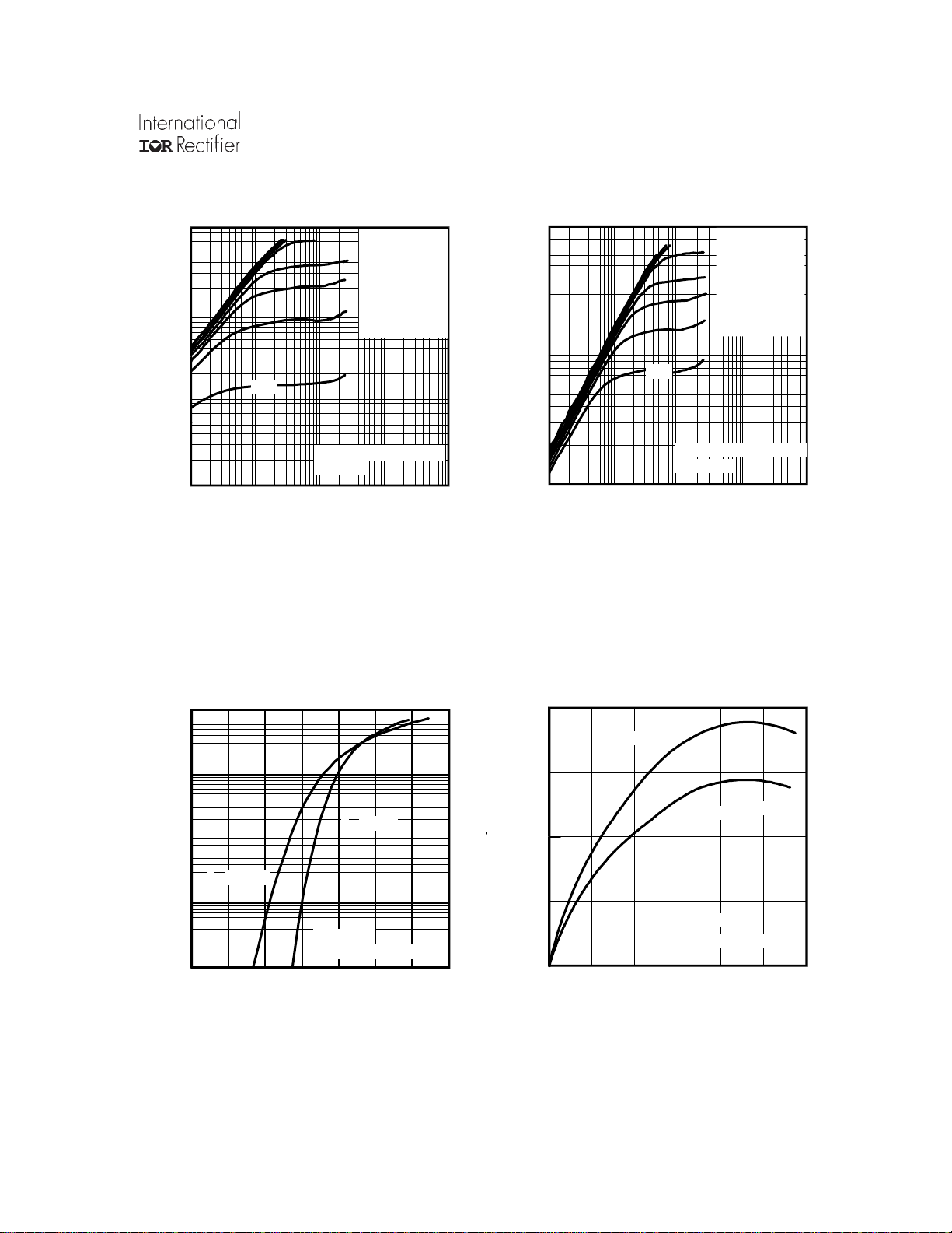
IRF2907ZS-7PPbF
1000
TOP 15V
)
A
(
t
n
e
r
100
r
u
C
e
c
r
u
o
S
o
t
-
10
n
i
a
r
D
,
D
I
4.5V
≤
BOTTOM 4.5V
60µs PULSE WIDTH
Tj = 25°C
1
0.1 1 10 100 1000
VDS, Drain-to-Source Voltage (V)
Fig 1. Typical Output Characteristics
VGS
10V
8.0V
7.0V
6.0V
5.5V
5.0V
1000
TOP 15V
)
A
(
t
n
e
r
r
u
C
e
c
r
u
o
S
o
t
n
i
a
r
D
,
I
100
4.5V
D
≤
BOTTOM 4.5V
60µs PULSE WIDTH
Tj = 175°C
10
0.1 1 10 100 1000
VDS, Drain-to-Source Voltage (V)
Fig 2. Typical Output Characteristics
VGS
10V
8.0V
7.0V
6.0V
5.5V
5.0V
1000
)
Α
(
t
100
n
e
r
r
u
C
e
c
r
10
u
o
S
o
t
n
i
a
r
D
,
D
I
TJ = 175°C
1
TJ = 25°C
V
= 25V
DS
≤
60µs PULSE WIDTH
0.1
1 2 3 4 5 6 7 8
VGS, Gate-to-Source Voltage (V)
Fig 3. Typical Transfer Characteristics
200
)
S
(
e
c
150
n
a
t
c
u
d
n
o
c
s
100
n
a
r
T
d
r
a
w
r
o
50
F
,
s
f
G
TJ = 25°C
TJ = 175°C
V
= 10V
DS
380µs PULSE WIDTH
0
0 25 50 75 100 125 150
ID,Drain-to-Source Current (A)
Fig 4. Typical Forward Transconductance
vs. Drain Current
www.irf.com 3
Page 4

IRF2907ZS-7PPbF
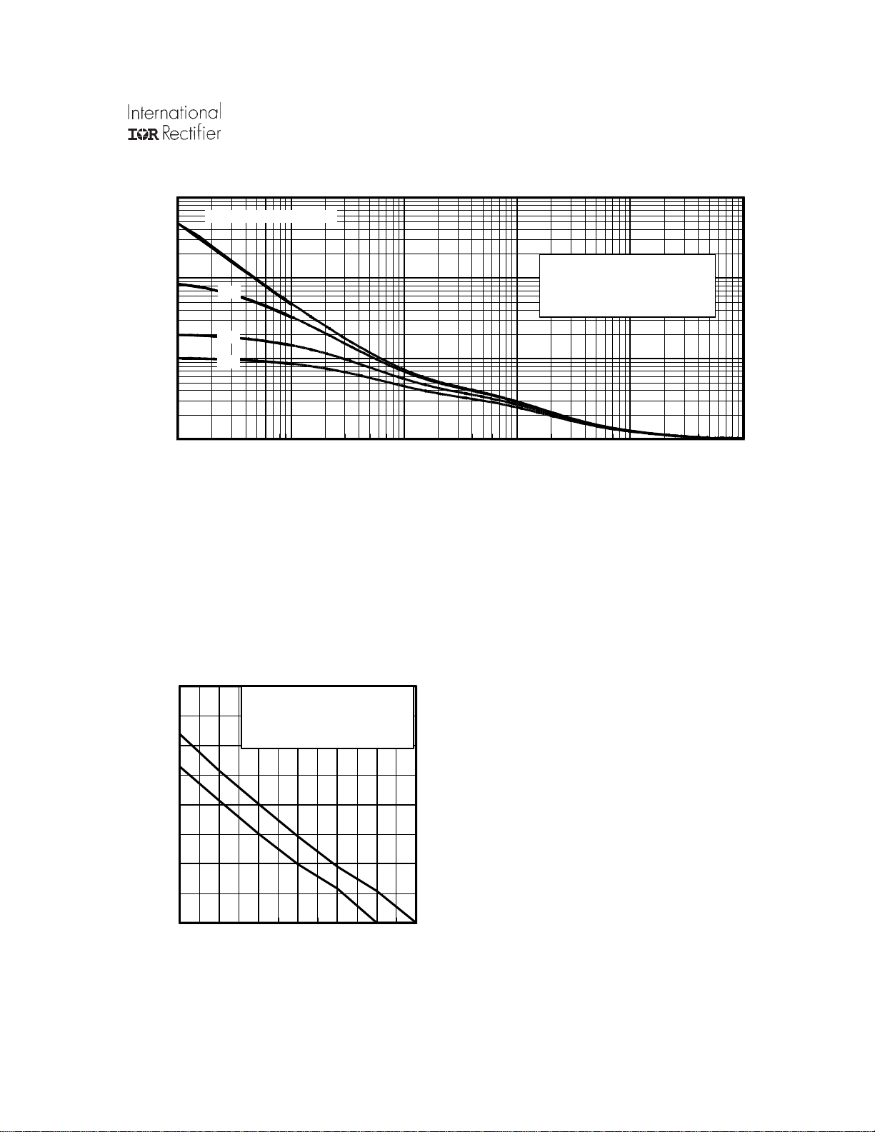
100000
)
F
10000
p
(
e
c
n
a
t
i
c
a
p
a
C
,
1000
C
100
V
= 0V, f = 1 MHZ
GS
C
= C
iss
rss
oss
= C
= C
gs
gd
ds
C
iss
C
oss
C
rss
C
C
1 10 100
VDS, Drain-to-Source Voltage (V)
Fig 5. Typical Capacitance vs.
Drain-to-Source Voltage
+ Cgd, C
+ C
gd
SHORTED
ds
12.0
ID= 110A
)
10.0
V
(
e
g
a
t
l
8.0
o
V
e
c
r
u
6.0
o
S
o
t
e
t
4.0
a
G
,
S
G
2.0
V
0.0
0 50 100 150 200
VDS= 60V
VDS= 38V
VDS= 15V
Q
Total Gate Charge (nC)
G
Fig 6. Typical Gate Charge vs.
Gate-to-Source Voltage
1000
)
A
(
t
100
n
e
r
r
u
C
n
i
a
r
10
D
e
s
r
e
v
e
R
,
1
D
S
I
0.1
TJ = 175°C
TJ = 25°C
0.0 0.2 0.4 0.6 0.8 1.0 1.2 1.4
VSD, Source-to-Drain Voltage (V)
Fig 7. Typical Source-Drain Diode
V
GS
= 0V
10000
OPERATION IN THIS AREA
)
A
1000
(
t
n
e
r
r
u
C
100
e
c
r
u
o
S
-
10
o
t
n
i
a
r
D
,
1
D
I
Tc = 25°C
Tj = 175°C
Single Pulse
0.1
0 1 10 100 1000
LIMITED BY RDS(on)
DC
VDS, Drain-to-Source Voltage (V)
Fig 8. Maximum Safe Operating Area
100µsec
1msec
10msec
Forward Voltage
4 www.irf.com
Page 5

IRF2907ZS-7PPbF
τ
200
Limited By Package
160
)
A
(
t
n
120
e
r
r
u
C
n
i
a
r
80
D
,
D
I
40
0
25 50 75 100 125 150 175
TC , Case Temperature (°C)
Fig 9. Maximum Drain Current vs.
Case Temperature
3.0
e
c
n
a
t
s
i
s
e
R
n
O
e
c
r
u
o
S
o
t
n
i
a
r
D
,
)
n
o
(
S
D
R
)
d
e
z
i
l
a
m
r
o
N
(
2.5
2.0
1.5
1.0
ID = 180A
V
= 10V
GS
0.5
-60 -40 -20 0 20 40 60 80 100120140160180
TJ , Junction Temperature (°C)
Fig 10. Normalized On-Resistance
vs. Temperature
1
D = 0.50
)
C
J
h
t
Z
(
e
s
n
o
p
s
e
R
l
a
m
r
e
0.001
h
T
0.1
0.01
0.20
0.10
0.05
0.02
0.01
SINGLE PULSE
( THERMAL RESPONSE )
τ
J
τ
J
τ
1
τ
1
Ci= τi/Ri
R
R
1
R
1
τ
R
2
3
R
2
2
τ
2
Ri (°C/W) τi (sec)
R
3
τ
C
0.1072 0.000896
τ
3
0.2787 0.009380
τ
3
0.1143 0.121118
Notes:
1. Duty Factor D = t1/t2
2. Peak Tj = P dm x Zthjc + Tc
0.0001
1E-006 1E-005 0.0001 0.001 0.01 0.1
t1 , Rectangular Pulse Duration (sec)
Fig 11. Maximum Effective Transient Thermal Impedance, Junction-to-Case
www.irf.com 5
Page 6

IRF2907ZS-7PPbF
A
15V
DRIVER
+
-
V
DD
R
V
20V
V
DS
G
GS
L
D.U.T
I
AS
Ω
0.01
t
p
Fig 12a. Unclamped Inductive Test Circuit
V
(BR)DSS
t
p
I
AS
Fig 12b. Unclamped Inductive Waveforms
Q
G
10 V
Q
GS
Q
GD
700
)
J
m
(
600
y
g
r
e
n
E
500
e
h
c
n
400
a
l
a
v
A
e
300
s
l
u
P
e
l
200
g
n
i
S
,
100
S
A
E
TOP 24A
BOTTOM 110A
0
25 50 75 100 125 150 175
Starting TJ , Junction Temperature (°C)
Fig 12c. Maximum Avalanche Energy
vs. Drain Current
I
D
34A
V
G
4.5
)
V
Charge
Fig 13a. Basic Gate Charge Waveform
Current Regulator
Same Type as D.U.T.
50KΩ
.2µF
12V
V
GS
.3µF
D.U.T.
3mA
I
G
Current Sampling Resistors
+
V
DS
-
I
D
Fig 13b. Gate Charge Test Circuit
4.0
(
e
g
a
t
l
3.5
o
V
d
l
o
3.0
h
s
e
r
h
t
2.5
e
t
a
G
)
2.0
h
t
(
S
G
1.5
V
ID = 250µA
ID = 1.0mA
ID = 1.0A
1.0
-75 -50 -25 0 25 50 75 100 125 150 175 200
TJ , Temperature ( °C )
Fig 14. Threshold Voltage vs. Temperature
6 www.irf.com
Page 7
1000
IRF2907ZS-7PPbF
Duty Cycle = Single Pulse
)
A
(
100
t
n
e
r
r
u
C
e
h
c
n
a
l
10
a
v
A
1
1.0E-06 1.0E-05 1.0E-04 1.0E-03 1.0E-02 1.0E-01
0.01
0.05
0.10
Allowed avalanche Current vs
avalanche pulsewidth, tav
assuming ∆ Tj = 25°C due to
avalanche losses
tav (sec)
Fig 15. Typical Avalanche Current vs.Pulsewidth
Notes on Repetitive Avalanche Curves , Figures 15, 16:
200
TOP Single Pulse
BOTTOM 1% Duty Cycle
)
J
m
150
(
y
g
r
e
n
E
e
h
100
c
n
a
l
a
v
A
,
R
50
A
E
0
25 50 75 100 125 150 175
ID = 110A
Starting TJ , Junction Temperature (°C)
Fig 16. Maximum Avalanche Energy
(For further info, see AN-1005 at www.irf.com)
1. Avalanche failures assumption:
Purely a thermal phenomenon and failure occurs at a
temperature far in excess of T
. This is validated for
jmax
every part type.
2. Safe operation in Avalanche is allowed as long asT
jmax
not exceeded.
3. Equation below based on circuit and waveforms shown in
Figures 12a, 12b.
4. P
= Average power dissipation per single
D (ave)
avalanche pulse.
5. BV = Rated breakdown voltage (1.3 factor accounts for
voltage increase during avalanche).
6. I
= Allowable avalanche current.
av
7. ∆T = Allowable rise in junction temperature, not to exceed
T
(assumed as 25°C in Figure 15, 16).
jmax
t
Average time in avalanche.
av =
D = Duty cycle in avalanche = t
Z
(D, tav) = Transient thermal resistance, see figure 11)
thJC
P
= 1/2 ( 1.3·BV·Iav) = DT/ Z
D (ave)
I
2DT/ [1.3·BV·Zth]
av =
E
= P
AS (AR)
·f
av
D (ave)·tav
thJC
vs. Temperature
www.irf.com 7
is
Page 8

IRF2907ZS-7PPbF
Reverse
Recovery
Current
Driver Gate Drive
P.W.
D.U.T. ISDWaveform
D.U.T. VDSWaveform
Inductor Curent
* V
GS
D.U.T
+
-
R
G
+
Circuit Layout Considerations
• Low Stray Inductance
• Ground Plane
-
• Low Leakage Inductance
Current Transformer
-
• dv/dt controlled by R
• Driver same type as D.U.T.
• ISD controlled by Duty Factor "D"
• D.U.T. - Device Under Test
G
+
V
DD
Re-Applied
Voltage
+
-
Period
Body Diode Forward
Current
di/dt
Diode Recovery
dv/dt
Body Diode Forward Drop
Ripple ≤ 5%
= 5V for Logic Level Devices
D =
P. W .
Period
VGS=10V
V
DD
I
SD
*
Fig 17. Peak Diode Recovery dv/dt Test Circuit for N-Channel
HEXFET® Power MOSFETs
R
D.U.T.
D
+
V
DD
-
V
DS
V
GS
R
G
10V
Pulse Width ≤ 1 µs
Duty Factor ≤ 0.1 %
Fig 18a. Switching Time Test Circuit
V
DS
90%
10%
V
GS
t
d(on)tr
t
d(off)tf
Fig 18b. Switching Time Waveforms
8 www.irf.com
Page 9

D2Pak - 7 Pin Package Outline
Dimensions are shown in millimeters (inches)
IRF2907ZS-7PPbF
D2Pak - 7 Pin Part Marking Information
14
www.irf.com 9
Page 10

IRF2907ZS-7PPbF
D2Pak - 7 Pin Tape and Reel
Data and specifications subject to change without notice.
This product has been designed and qualified for the Automotive [Q101] market.
Qualification Standards can be found on IRs Web site.
IR WORLD HEADQUARTERS: 233 Kansas St., El Segundo, California 90245, USA Tel: (310) 252-7105
TAC Fax: (310) 252-7903
Visit us at www.irf.com for sales contact information. 08/05
10 www.irf.com
 Loading...