

Page 1
October 1997
Semiconductor
IRF220, IRF221,
IRF222, IRF223
4.0A and 5.0A, 150V and 200V, 0.8 and 1.2 Ohm,
N-Channel Power MOSFETs
Features
• 4.0A and 5.0A, 150V and 200V
•r
• SOA is Power Dissipation Limited
• Nanosecond Switching Speeds
• Linear Transfer Characteristics
• High Input Impedance
• Majority Carrier Device
• Related Literature
- TB334 “Guidelines for Soldering Surface Mount
= 0.8Ω and 1.2Ω
DS(ON)
Components to PC Boards”
Ordering Information
PART NUMBER PACKAGE BRAND
IRF220 TO-204AA IRF220
IRF221 TO-204AA IRF221
IRF222 TO-204AA IRF222
IRF223 TO-204AA IRF223
Description
These are N-Channel enhancement mode silicon gate
power field effect transistors. They are advanced power
MOSFETs designed, tested, and guaranteed to withstand a
specified level of energy in the breakdown avalanche mode
of operation. All of these power MOSFETs are designed for
applications such as switching regulators, switching convertors, motor drivers, relay drivers, and drivers for high power
bipolar switching transistors requiring high speed and low
gate drive power. These types can be operated directly from
integrated circuits.
Formerly developmental type TA09600.
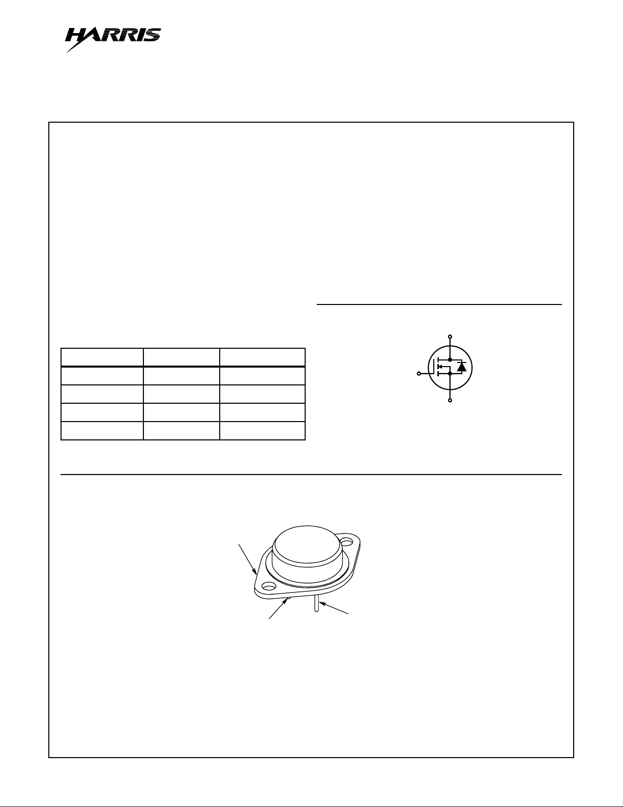
Symbol
D
G
S
NOTE: When ordering, use the entire part number.
Packaging
DRAIN
(FLANGE)
JEDEC TO-204AA
GATE (PIN 1)
SOURCE (PIN 2)
CAUTION: These devices are sensitive to electrostatic discharge. Users should follow proper ESD Handling Procedures.
Copyright
© Harris Corporation 199&
1
File Number 1567.2
Page 2
IRF220, IRF221, IRF222, IRF223
Absolute Maximum Ratings T
= 25oC, Unless Otherwise Specified
C
IRF220 IRF221 IRF222 IRF223 UNITS
Drain to Source Voltage (Note 1) . . . . . . . . . . . . . . . . . . .V
Drain to Gate Voltage (RGS = 20kΩ) (Note 1) . . . . . . . V
DGR
Continuous Drain Current. . . . . . . . . . . . . . . . . . . . . . . . . . I
TC= 100oC. . . . . . . . . . . . . . . . . . . . . . . . . . . . . . . . . . . I
Pulsed Drain Current (Note 3) . . . . . . . . . . . . . . . . . . . . . I
Gate to Source Voltage . . . . . . . . . . . . . . . . . . . . . . . . . .V
Maximum Power Dissipation . . . . . . . . . . . . . . . . . . . . . . .P
DS
D
D
DM
GS
D
200 150 200 150 V
200 150 200 150 V
5.0
3.0
5.0
3.0
4.0
2.5
4.0
2.5
20 20 16 16 A
±20 ±20 ±20 ±20 V
40 40 40 40 W
A
A
Linear Derating Factor . . . . . . . . . . . . . . . . . . . . . . . . . . . . . . 0.32 0.32 0.32 0.32 W/oC
Single Pulse Avalanche Rating. . . . . . . . . . . . . . . . . . . . .E
Operating and Storage Temperature . . . . . . . . . . . .TJ,T
AS
STG
Maximum Temperature for Soldering
Leads at 0.063in (1.6mm) from Case for 10s . . . . . . . . . T
Package Body for 10s, See Techbrief 334 . . . . . . . . . T
CAUTION: Stresses above those listed in “Absolute Maximum Ratings” may cause permanent damage to the device. This is a stress only rating and operation
of the device at these or any other conditions above those indicated in the operational sections of this specification is not implied.
L
pkg
85 85 85 85 mJ
-55 to 150 -55 to 150 -55 to 150 -55 to 150
300
260
300
260
300
260
300
260
o
C
o
C
o
C
NOTE:
1. TJ= 25oC to 125oC.
Electrical Specifications T
= 25oC, Unless Otherwise Specified
C
PARAMETER SYMBOL TEST CONDITIONS MIN TYP MAX UNITS
Drain to Source Breakdown Voltage BV
DSSID
= 250µA, VGS = 0V, (Figure 10)
IRF220, IRF222 200 - - V
IRF221, IRF223 150 - - V
Gate Threshold Voltage V
Zero Gate Voltage Drain Current I
On-State Drain Current (Note 2) I
GS(TH)VDS
DSSVDS
D(ON)VDS
= VGS, ID = 250µA 2.0 - 4.0 V
= Rated BV
VDS = 0.8 x Rated BV
> I
D(ON)
, VGS = 0V - - 25 µA
DSS
, VGS = 0V, TJ = 125oC - - 250 µA
DSS
x r
DS(ON)MAX
, VGS = 10V
IRF220, IRF221 5.0 - - A
IRF222, IRF223 4.0 - - A
Gate to Source Leakage Current I
Drain to Source On Resistance (Note 2) r
GSSVGS
DS(ON)ID
= ±20V - - ±100 nA
= 2.5A, VGS = 10V, (Figure 8)
IRF220, IRF221 - 0.5 0.8 Ω
IRF222, IRF223 - 0.8 1.2 Ω
Forward Transconductance (Note 2) g
Turn-On Delay Time t
d(ON)VDD
VDS > I
fs
= 0.5 x Rated BV
D(ON)
x r
DS(ON)MAX
, ID = 2.5A 1.3 2.5 - S
, ID≈ 2.5A, RG = 50Ω
DSS
-2040ns
For IRF220, 222 RL = 80Ω
Rise Time t
Turn-Off Delay Time t
d(OFF)
Fall Time t
Total Gate Charge
Q
g(TOT)VGS
(Gate to Source + Gate to Drain)
For IRF221, 223 RL = 60Ω
r
(Figures 17, 18) MOSFET Switching Times are
Essentially Independent of Operating
Temperature
f
= 10V, ID = 6.0A, VDS = 0.8 x Rated BV
I
= 1.5mA, (Figures 14, 19, 20) Gate
g(REF)
DSS
-3060ns
- 50 100 ns
-3060ns
-1115nC
Charge is Essentially Independent of Operating
Gate to Source Charge Q
Gate to Drain “Miller” Charge Q
gs
gd
Temperature
- 5.0 - nC
- 6.0 - nC
2
Page 3
IRF220, IRF221, IRF222, IRF223
Electrical Specifications T
= 25oC, Unless Otherwise Specified (Continued)
C
PARAMETER SYMBOL TEST CONDITIONS MIN TYP MAX UNITS
Input Capacitance C
Output Capacitance C
Reverse Transfer Capacitance C
Internal Drain Inductance L
Internal Source Inductance L
Thermal Resistance Junction to Case R
Thermal Resistance Junction to Ambient R
Source to Drain Diode Specifications
PARAMETER SYMBOL TEST CONDITIONS MIN TYP MAX UNITS
ISSVDS
= 25V, VGS = 0V, f = 1MHz
- 450 - pF
(Figure 11)
OSS
RSS
Measured Between the
D
Contact Screw on the
Flange that is Closer to
Source and Gate Pins and
the Center of Die
Measured From the
S
Modified MOSFET
Symbol Showing the
Internal Device
Inductances
D
L
D
- 150 - pF
-40-pF
- 5.0 - nH
- 12.5 - nH
Source Lead, 6mm
(0.25in) From the Flange
and the Source Bonding
Pad
θJC
Free Air Operation - - 30oC/W
θJA
G
L
S
S
- - 3.12oC/W
Continuous Source to Drain Current I
IRF220, IRF221 - - 5.0 A
IRF222, IRF223 - - 4.0 A
Pulse Source to Drain Current (Note 3) I
Modified MOSFET
SD
Symbol Showing the
Integral Reverse
P-N Junction Rectifier
SDM
D
G
IRF220, IRF221 - - 20 A
IRF222, IRF223 - - 16 A
S
Source to Drain Diode Voltage (Note 2) V
SD
IRF220, IRF221 TC = 25oC, ISD = 5.0A, VGS = 0V, (Figure 13) - - 2.0 V
IRF222, IRF223 TC = 25oC, ISD = 4.0A, VGS = 0V, (Figure 13) - - 1.8 V
Reverse Recovery Time t
Reverse Recovery Charge Q
TJ = 150oC, ISD = 5.0A, dISD/dt = 100A/µs - 350 - ns
rr
TJ = 150oC, ISD = 5.0A, dISD/dt = 100A/µs - 2.3 - µC
RR
NOTES:
2. Pulse test: pulse width ≤ 300µs, duty cycle ≤ 2%.
3. Repetitive rating: pulse width limited by maximum junction temperature. See Transient Thermal Impedance curve (Figure 3).
4. VDD= 10V, starting TJ= 25oC, L = 6.18mH, RG= 50Ω, peak IAS = 5A. See Figures 15, 16.
3
Page 4
IRF220, IRF221, IRF222, IRF223
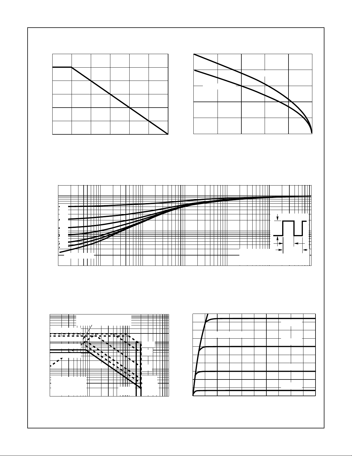
Typical Performance Curves
1.2
1.0
0.8
0.6
0.4
0.2
POWER DISSIPATION MULTIPLIER
0
0 50 100 150
TC, CASE TEMPERATURE (oC)
Unless Otherwise Specified
FIGURE 1. NORMALIZED POWER DISSIPATION vs
CASE TEMPERATURE
1.0
5
4
3
IRF222, IRF223
2
, DRAIN CURRENT (A)
D
I
1
0
25 50 75 100
TC, CASE TEMPERATURE (oC)
IRF220, IRF221
125
FIGURE 2. MAXIMUM CONTINUOUS DRAIN CURRENT vs
CASE TEMPERATURE
150
0.5
0.2
0.1
0.1
0.05
THERMAL IMPEDANCE
0.01
0.02
0.01
SINGLE PULSE
-5
10
-4
10
-3
10
t1, RECTANGULAR PULSE DURATION (s)
, NORMALIZED TRANSIENT
θJC
Z
FIGURE 3. NORMALIZED MAXIMUM TRANSIENT THERMAL IMPEDANCE
100
IRF220, IRF221
IRF222, IRF223
10
IRF220, IRF221
IRF222, IRF223
1.0
, DRAIN CURRENT (A)
D
I
TC = 25oC
= MAX RATED
T
J
SINGLE PULSE
0.1
1.0 10 100 1000
OPERATION IN THIS AREA
IS LIMITED BY r
VDS, DRAIN TO SOURCE VOLTAGE (V)
DC
DS(ON)
IRF221
IRF223
100µs
10µs
1ms
10ms
100ms
IRF220
IRF222
P
DM
t
1
t
x R
θJC
VGS = 7V
VGS = 6V
VGS = 5V
VGS = 4V
2
2
NOTES:
DUTY FACTOR: D = t1/t
PEAK TJ = PDM x Z
-2
10
10
10V
8
6
4
, DRAIN CURRENT (A)
D
I
2
0
0 20 40 60 80 100
-1
10
80µs PULSE TEST
, DRAIN TO SOURCE VOLTAGE (V)
V
DS
1
θJC
+ T
C
10
FIGURE 4. FORWARD BIAS SAFE OPERATING AREA FIGURE 5. OUTPUT CHARACTERISTICS
4
Page 5

IRF220, IRF221, IRF222, IRF223
Typical Performance Curves
5
4
3
2
, DRAIN CURRENT (A)
D
I
1
0
0 24 6810
10V
6V
VGS = 5V
V
, DRAIN TO SOURCE VOLTAGE (V)
DS
Unless Otherwise Specified (Continued)
80µs PULSE TEST
8V
4V
FIGURE 6. SATURATION CHARACTERISTICS FIGURE 7. TRANSFER CHARACTERISTICS
1.5
1.0
VGS = 10V
10
80µs PULSE TEST
V
>I
D(ON)
= 25oC
J
= -55oC
J
V
VGS = 10V
ID = 2A
x r
GS
DS
8
6
4
, DRAIN CURRENT (A)
D
TJ = 125oC
I
2
T
T
0
024 6810
2.2
1.8
1.4
MAX
DS(ON)
, GATE TO SOURCE VOLTAGE (V)
, DRAIN TO SOURCE
0.5
ON RESISTANCE (Ω)
DS(ON)
r
0
0 5 10 15 20
, DRAIN CURRENT (A)
I
D
VGS = 20V
NOTE: Heating effect of 2µs is minimal.
FIGURE 8. DRAIN TO SOURCE ON RESISTANCE vs GATE
VOLTAGE AND DRAIN CURRENT
1.25
ID = 250µA
1.15
1.05
0.95
BREAKDOWN VOLTAGE
0.85
NORMALIZED DRAIN TO SOURCE
0.75
-40 0 40 80 120 160
TJ, JUNCTION TEMPERATURE (oC)
1.0
ON RESISTANCE
0.6
NORMALIZED DRAIN TO SOURCE
0.2
-40 0 40 80 120
T
, JUNCTION TEMPERATURE (oC)
J
FIGURE 9. NORMALIZED DRAIN TO SOURCE ON
RESISTANCE vs JUNCTION TEMPERATURE
1000
VGS = 0V, f = 1MHz
C
= CGS + C
ISS
C
800
600
C
400
C, CAPACITANCE (pF)
200
0
01020304050
ISS
C
OSS
C
RSS
VDS, DRAIN TO SOURCE VOLTAGE (V)
C
RSS
OSS
= C
GD
≈ CDS + C
GD
GD
FIGURE 10. NORMALIZED DRAIN TO SOURCE BREAKDOWN
VOLTA GE vs JUNCTION TEMPERATURE
FIGURE 11. CAPACITANCE vs DRAIN TO SOURCE VOLTAGE
5
Page 6

IRF220, IRF221, IRF222, IRF223
Typical Performance Curves
5
VDS > I
80µs PULSE TEST
4
3
2
, TRANSCONDUCTANCE (S)
1
fs
g
0
0246 810
D(ON)
x r
DS(ON)MAX
I
, DRAIN CURRENT (A)
D
Unless Otherwise Specified (Continued)
2
TJ = -55oC
TJ = 25oC
TJ = 125oC
100
10
TJ = 150oC
, SOURCE TO DRAIN CURRENT (A)
SD
I
1.0
01 23 4
TJ = 25oC
TJ = 25oC
VSD, SOURCE TO DRAIN VOLTAGE (V)
FIGURE 12. TRANSCONDUCTANCE vs DRAIN CURRENT FIGURE 13. SOURCE TO DRAIN DIODE VOLTAGE
20
ID = 6.0A
15
VDS = 100V
VDS = 40V
TJ = 150oC
10
5
, GATE TO SOURCE VOLTAGE (V)
GS
V
0
048121620
TOTAL GATE CHARGE (nC)
Q
g(TOT),
VDS = 160V
IRF220, IRF222
FIGURE 14. GATE TO SOURCE VOLTAGE vs GATE CHARGE
6
Page 7

IRF220, IRF221, IRF222, IRF223
Test Circuits and Waveforms
V
DS
BV
DSS
L
VARY t
TO OBTAIN
P
REQUIRED PEAK I
V
GS
AS
R
G
+
V
DD
-
DUT
0V
P
I
AS
0.01Ω
0
t
FIGURE 15. UNCLAMPED ENERGY TEST CIRCUIT FIGURE 16. UNCLAMPED INDUCTIVE WAVEFORMS
t
P
I
AS
t
AV
V
DS
V
DD
t
ON
t
d(ON)
t
R
L
+
V
R
G
DD
-
V
DS
0
r
90%
10%
DUT
V
GS
V
GS
10%
0
50%
PULSE WIDTH
FIGURE 17. SWITCHING TIME TEST CIRCUIT FIGURE 18. RESISTIVE SWITCHING WAVEFORMS
V
DS
(ISOLATED
SUPPLY)
SAME TYPE
AS DUT
V
DD
Q
g(TOT)
Q
gd
Q
gs
12V
BATTERY
0.2µF
50kΩ
CURRENT
REGULATOR
0.3µF
t
d(OFF)
90%
V
GS
t
OFF
50%
t
f
10%
90%
G
I
0
g(REF)
IG CURRENT
SAMPLING
RESISTOR RESISTOR
FIGURE 19. GATE CHARGE TEST CIRCUIT
D
S
CURRENT
I
D
SAMPLING
DUT
V
DS
0
I
V
DS
G(REF)
0
FIGURE 20. GATE CHARGE WAVEFORMS
7
 Loading...