

Page 1
PD - 93907
AUTOMOTIVE MOSFET
Typical Applications
● Integrated Starter Alternator
● 42 Volts Automotive Electrical Systems
IRF1407
HEXFET® Power MOSFET
D
V
= 75V
DSS
Benefits
● Advanced Process Technology
● Ultra Low On-Resistance
● Dynamic dv/dt Rating
● 175°C Operating Temperature
● Fast Switching
● Repetitive Avalanche Allowed up to Tjmax
G
S
R
DS(on)
ID = 130AV
= 0.0078Ω
Description
Specifically designed for Automotive applications, this Stripe Planar
design of HEXFET
techniques to achieve extremely low on-resistance per silicon area.
Additional features of this HEXFET power MOSFET are a 175°C junction
operating temperature, fast switching speed and improved repetitive
avalanche rating. These benefits combine to make this design an extremely
efficient and reliable device for use in Automotive applications and a wide
variety of other applications.
®
Power MOSFETs utilizes the lastest processing
TO-220AB
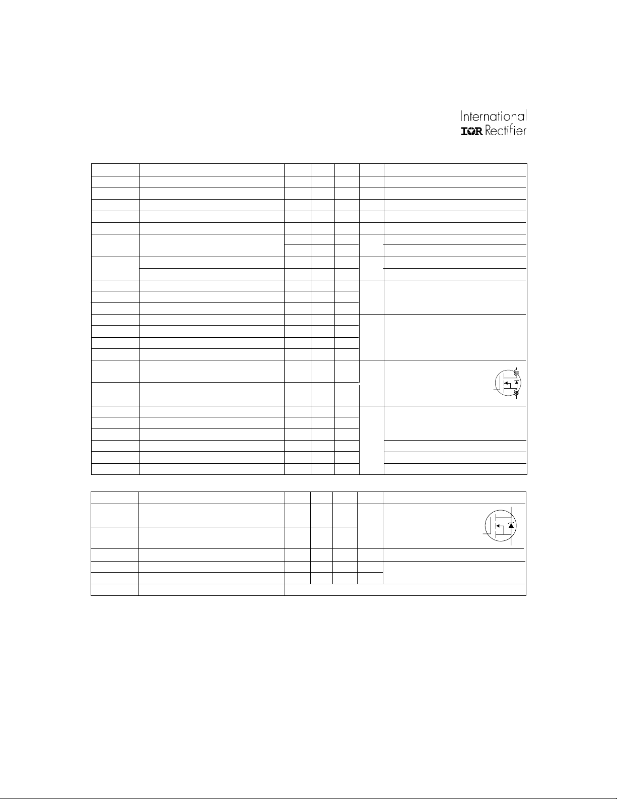
Absolute Maximum Ratings
Parameter Max. Units
ID @ TC = 25°C Continuous Drain Current, VGS @ 10V 130V
ID @ TC = 100°C Continuous Drain Current, VGS @ 10V 92V A
I
DM
PD @TC = 25°C Power Dissipation 330 W
V
GS
E
AS
I
AR
E
AR
dv/dt Peak Diode Recovery dv/dt S 4.6 V/ns
T
J
T
STG
Pulsed Drain Current Q 520
Linear Derating Factor 2.2 W/°C
Gate-to-Source Voltage ± 20 V
Single Pulse Avalanche EnergyR 390 mJ
Avalanche CurrentQ See Fig.12a, 12b, 15, 16 A
Repetitive Avalanche EnergyW mJ
Operating Junction and -55 to + 175
Storage Temperature Range
Soldering Temperature, for 10 seconds 300 (1.6mm from case )
Mounting Torque, 6-32 or M3 screw 10 lbf•in (1.1N•m)
°C
Thermal Resistance
Parameter Typ. Max. Units
R
θJC
R
θCS
R
θJA
Junction-to-Case ––– 0.45
Case-to-Sink, Flat, Greased Surface 0.50 ––– °C/W
Junction-to-Ambient ––– 62
www.irf.com 1
10/11/01
Page 2
IRF1407
Electrical Characteristics @ TJ = 25°C (unless otherwise specified)
Parameter Min. Typ. Max. Units Conditions
V
(BR)DSS
∆V
(BR)DSS
R
DS(on)
V
GS(th)
g
fs
I
DSS
I
GSS
Q
g
Q
gs
Q
gd
t
d(on)
t
r
t
d(off)
t
f
L
D
L
S
C
iss
C
oss
C
rss
C
oss
C
oss
C
eff. Effective Output Capacitance U ––– 1100 ––– VGS = 0V, VDS = 0V to 60V
oss
Source-Drain Ratings and Characteristics
I
S
I
SM
V
SD
t
rr
Q
rr
t
on
Notes:
Q Repetitive rating; pulse width limited by
max. junction temperature. (See fig. 11).
R Starting T
RG = 25Ω, I
S I
SD
TJ ≤ 175°C
T Pulse width ≤ 400µs; duty cycle ≤ 2%.
Drain-to-Source Breakdown Voltage 75 ––– ––– VVGS = 0V, ID = 250µA
/∆T
Breakdown Voltage Temp. Coefficient ––– 0.09 ––– V/°C Reference to 25°C, ID = 1mA
J
Static Drain-to-Source On-Resistance ––– ––– 0.0078 Ω VGS = 10V, ID = 78A T
Gate Threshold Voltage 2.0 ––– 4.0 V VDS = 10V, ID = 250µA
Forward Transconductance 74 ––– ––– SVDS = 25V, ID = 78A
Drain-to-Source Leakage Current
––– ––– 20
––– ––– 250 VDS = 60V, VGS = 0V, TJ = 150°C
Gate-to-Source Forward Leakage ––– ––– 200 VGS = 20V
Gate-to-Source Reverse Leakage ––– ––– -200
VDS = 75V, VGS = 0V
µA
nA
VGS = -20V
Total Gate Charge ––– 160 250 ID = 78A
Gate-to-Source Charge ––– 35 52 nC VDS = 60V
Gate-to-Drain ("Miller") Charge ––– 54 81 VGS = 10VT
Turn-On Delay Time ––– 11 ––– VDD = 38V
Rise Time ––– 150 ––– ID = 78A
Turn-Off Delay Time ––– 150 ––– RG = 2.5Ω
ns
Fall Time ––– 140 ––– VGS = 10V T
4.5
Internal Drain Inductance
Internal Source Inductance ––– –––
––– –––
7.5
Between lead,
6mm (0.25in.)
nH
from package
and center of die contact
Input Capacitance ––– 5600 ––– VGS = 0V
Output Capacitance ––– 890 ––– pF VDS = 25V
Reverse Transfer Capacitance ––– 190 ––– ƒ = 1.0KHz, See Fig. 5
Output Capacitance ––– 5800 ––– VGS = 0V, VDS = 1.0V, ƒ = 1.0KHz
Output Capacitance ––– 560 ––– VGS = 0V, VDS = 60V, ƒ = 1.0KHz
Parameter Min. Typ. Max. Units Conditions
Continuous Source Current MOSFET symbol
(Body Diode)
Pulsed Source Current integral reverse
(Body Diode) Q
––– –––
––– –––
130V
520
showing the
A
p-n junction diode.
Diode Forward Voltage ––– ––– 1.3 V TJ = 25°C, IS = 78A, VGS = 0VT
Reverse Recovery Time ––– 110 170 ns TJ = 25°C, IF = 78A
Reverse RecoveryCharge ––– 390 5 90 nC di/dt = 100A/µs
Forward Turn-On Time Intrinsic turn-on time is negligible (turn-on is dominated by LS+LD)
U C
eff. is a fixed capacitance that gives the same charging time
oss
= 25°C, L = 0.13mH
J
= 78A. (See Figure 12).
AS
≤ 78A, di/dt ≤ 320A/µs, V
DD
≤ V
(BR)DSS
as C
VCalculated continuous current based on maximum allowable
junction temperature. Package limitation current is 75A.
,
WLimited by T
oss
while V
is rising from 0 to 80% V
DS
, see Fig.12a, 12b, 15, 16 for typical repetitive
Jmax
avalanche performance.
T
DSS
D
G
S
D
G
S
.
2 www.irf.com
Page 3
IRF1407
(
)
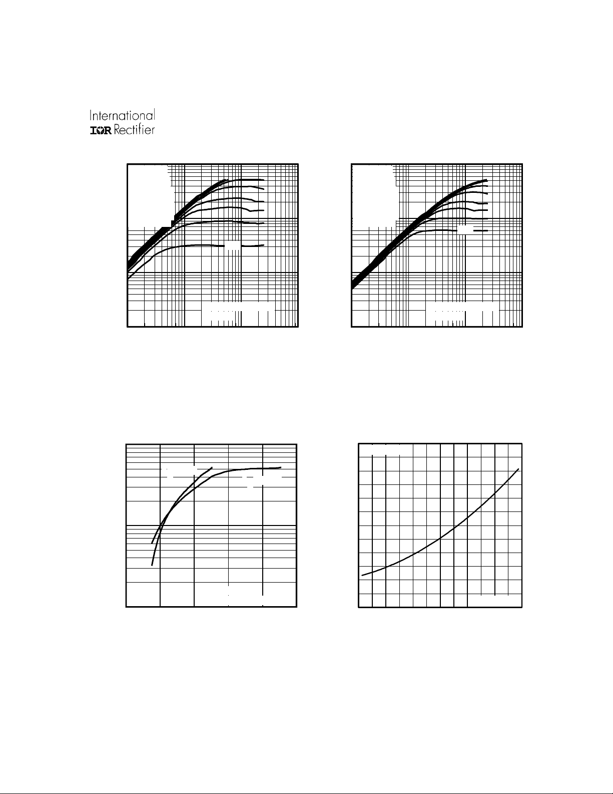
1000
100
VGS
TOP 15V
10V
8.0V
7.0V
6.0V
5.5V
5.0V
BOTTOM 4.5V
4.5V
10
, Drain-to-Source Current (A)
D
I
20µs PULSE WIDTH
Tj = 25°C
1
0.1 1 10 100
VDS, Drain-to-Source Voltage (V)
1000.00
1000
100
10
, Drain-to-Source Current (A)
D
I
VGS
TOP 15V
10V
8.0V
7.0V
6.0V
5.5V
5.0V
BOTTOM 4.5V
4.5V
20µs PULSE WIDTH
Tj = 175°C
1
0.1 1 10 100
VDS, Drain-to-Source Voltage (V)
Fig 2. Typical Output CharacteristicsFig 1. Typical Output Characteristics
3.0
130A
I =
D
)
(Α
100.00
, Drain-to-Source Current
D
I
10.00
3.0 5.0 7.0 9.0 11.0 13.0
Fig 3. Typical Transfer Characteristics
TJ = 25°C
TJ = 175°C
V
= 15V
DS
20µs PULSE WIDTH
VGS, Gate-to-Source Voltage (V)
2.5
2.0
1.5
(Normalized)
1.0
0.5
DS(on)
R , Drain-to-Source On Resistance
0.0
-60 -40 -20 0 20 40 60 80 100 120 140 160 180
T , Junction Temperature
J
Fig 4. Normalized On-Resistance
V =
10V
GS
°
C
vs. Temperature
www.irf.com 3
Page 4
IRF1407
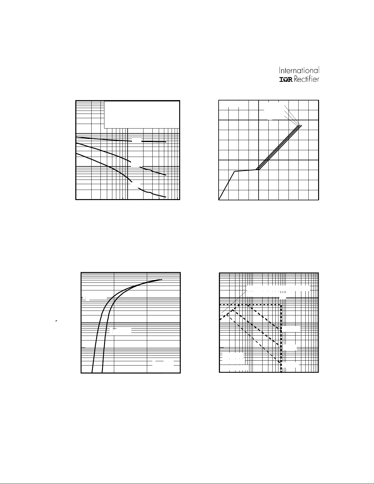
)
100000
10000
V
= 0V, f = 1 MHZ
GS
C
= C
iss
gs
C
= C
rss
gd
C
= C
ds
+ C
oss
+ Cgd, C
gd
Ciss
1000
C, Capacitance(pF)
Coss
Crss
100
1 10 100
VDS, Drain-to-Source Voltage (V)
Fig 5. Typical Capacitance vs.
Drain-to-Source Voltage
1000.00
SHORTED
ds
15
D
I =
78A
12
9
6
3
GS
V , Gate-to-Source Voltage (V)
0
0 40 80 120 160 200
Q , Total Gate Charge (nC
G
V = 60V
DS
V = 37V
DS
V = 15V
DS
Fig 6. Typical Gate Charge vs.
Gate-to-Source Voltage
10000
OPERATION IN THIS AREA
100.00
TJ = 175°C
10.00
TJ = 25°C
, Reverse Drain Current (A)
1.00
SD
I
0.10
0.0 1.0 2.0 3.0
VSD, Source-toDrain Voltage (V)
Fig 7. Typical Source-Drain Diode
V
GS
= 0V
1000
100
10
, Drain-to-Source Current (A)
D
I
Tc = 25°C
Tj = 175°C
Single Pulse
1
1 10 100 1000
Fig 8. Maximum Safe Operating Area
LIMITED BY RDS(on)
V
, Drain-toSource Voltage (V)
DS
100µsec
1msec
10msec
Forward Voltage
4 www.irf.com
Page 5
IRF1407
140
LIMITED BY PACKAGE
120
100
80
60
D
40
I , Drain Current (A)
20
0
25 50 75 100 125 150 175
T , Case Temperature ( C)
C
°
Fig 9. Maximum Drain Current vs.
Case Temperature
1
R
V
DS
V
GS
R
G
D
D.U.T.
10V
Pulse Width ≤ 1 µs
Duty Factor ≤ 0.1 %
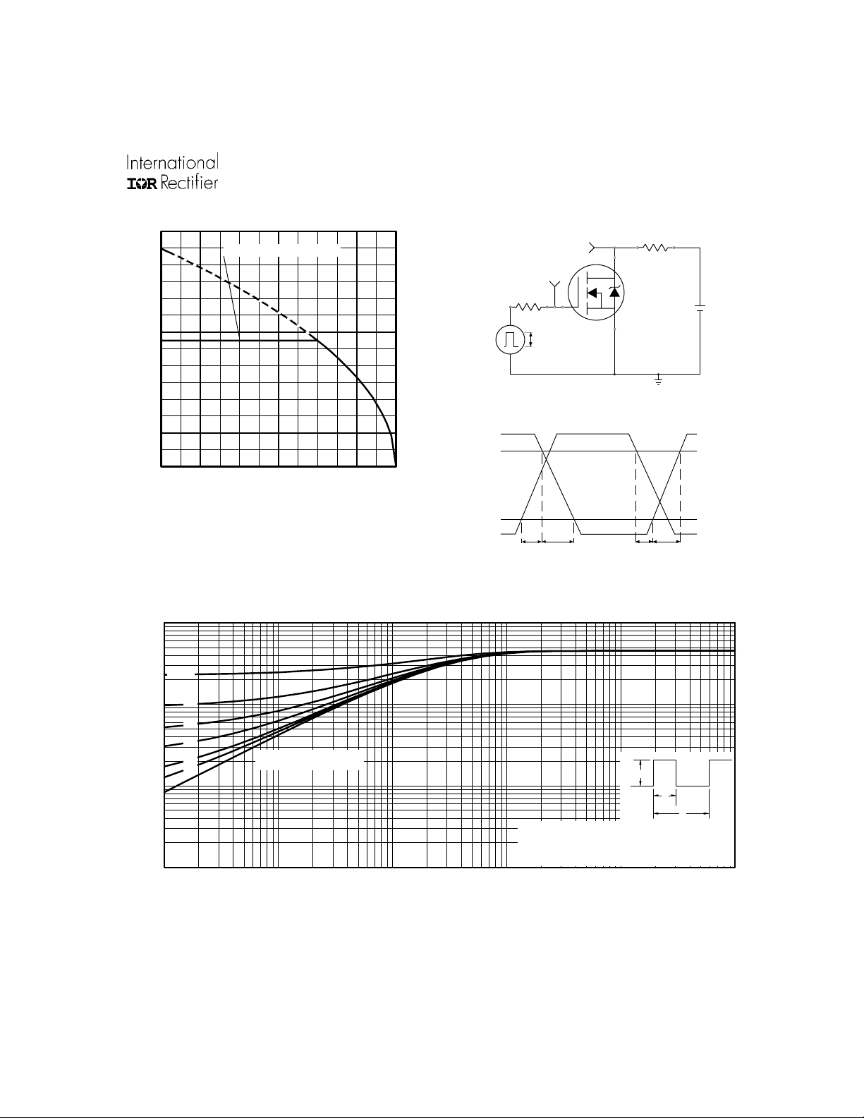
Fig 10a. Switching Time Test Circuit
V
DS
90%
10%
V
GS
t
d(on)tr
t
d(off)tf
Fig 10b. Switching Time Waveforms
+
V
DD
-
D = 0.50
thJC
Thermal Response (Z )
0.001
0.20
0.1
0.10
0.05
0.02
0.01
0.01
0.00001 0.0001 0.001 0.01 0.1 1
SINGLE PULSE
(THERMAL RESPONSE)
t , Rectangular Pulse Duration (sec)
1
P
DM
t
Notes:
1. Duty factor D = t / t
2. Peak T = P x Z + T
1 2
J DM thJC C
1
t
2
Fig 11. Maximum Effective Transient Thermal Impedance, Junction-to-Case
www.irf.com 5
Page 6

IRF1407
A
(
)
15V
DRIVER
+
-
V
R
20V
V
DS
G
L
D.U.T
I
AS
0.01
t
p
Ω
Fig 12a. Unclamped Inductive Test Circuit
V
(BR)DSS
t
p
I
AS
Fig 12b. Unclamped Inductive Waveforms
Q
G
10 V
Q
GS
Q
GD
DD
650
TOP
520
390
260
130
AS
E , Single Pulse Avalanche Energy (mJ)
0
25 50 75 100 125 150 175
Starting T , Junction Temperature
J
BOTTOM
Fig 12c. Maximum Avalanche Energy
vs. Drain Current
3.5
C
I
D
32A
55A
78A
°
V
G
3.0
Charge
Fig 13a. Basic Gate Charge Waveform
Current Regulator
Same Type as D.U.T.
2.5
ID = 250µA
Gate threshold Voltage (V)
50KΩ
.2µF
12V
V
GS
.3µF
D.U.T.
3mA
I
G
Current Sampling Resistors
+
V
-
I
D
Fig 13b. Gate Charge Test Circuit
DS
2.0
GS(th)
V
1.5
-75 -50 -25 0 25 50 75 100 125 150 175 200
TJ , Temperature ( °C )
Fig 14. Threshold Voltage vs. Temperature
6 www.irf.com
Page 7
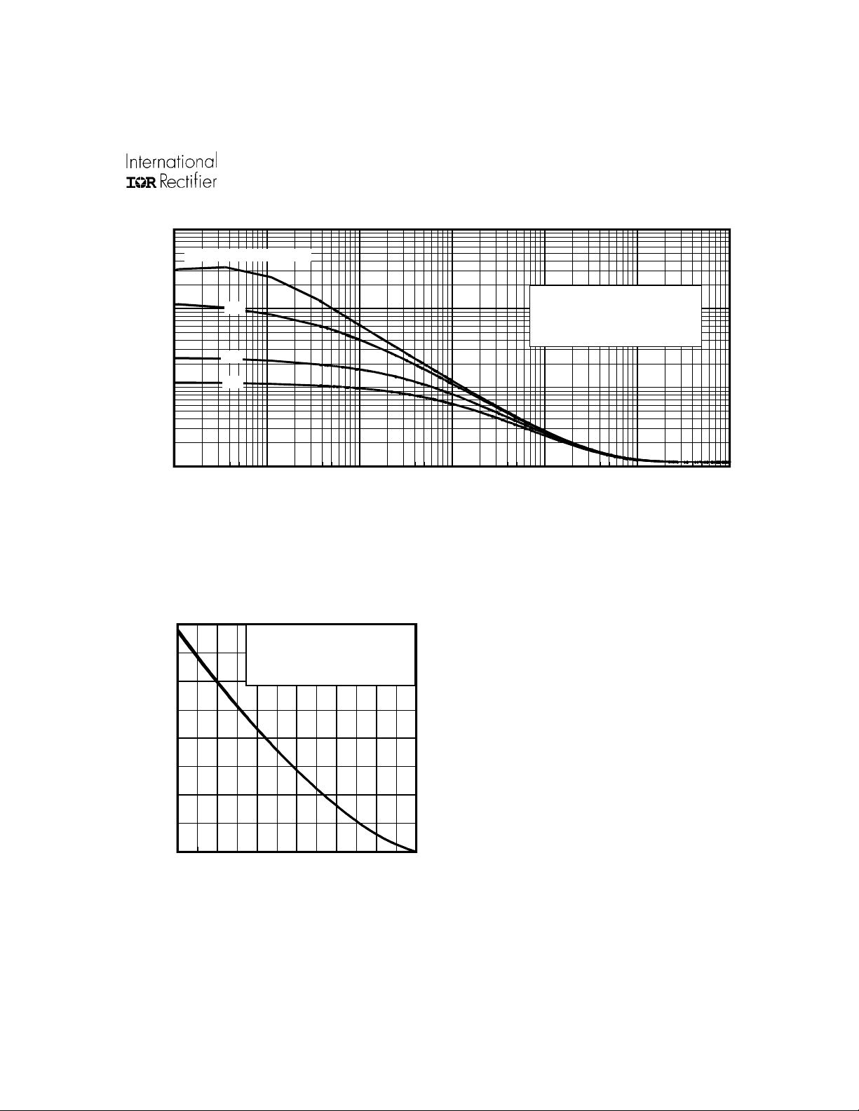
1000
Duty Cycle = Single Pulse
100
0.01
0.05
IRF1407
Allowed avalanche Current vs
avalanche pulsewidth, tav
assuming ∆Tj = 25°C due to
avalanche losses
10
0.10
Avalanche Current (A)
1
1.0E-07 1.0E-06 1.0E-05 1.0E-04 1.0E-03 1.0E-02 1.0E-01
tav (sec)
Fig 15. Typical Avalanche Current vs.Pulsewidth
400
TOP Single Pulse
BOTTOM 10% Duty Cycle
ID = 78A
300
200
, Avalanche Energy (mJ)
100
AR
E
0
25 50 75 100 125 150 175
Starting TJ , Junction Temperature (°C)
Notes on Repetitive Avalanche Curves , Figures 15, 16:
(For further info, see AN-1005 at www.irf.com)
1. Avalanche failures assumption:
Purely a thermal phenomenon and failure occurs at a
temperature far in excess of T
. This is validated for
jmax
every part type.
2. Safe operation in Avalanche is allowed as long asT
not exceeded.
3. Equation below based on circuit and waveforms shown in
Figures 12a, 12b.
4. P
= Average power dissipation per single
D (ave)
avalanche pulse.
5. BV = Rated breakdown voltage (1.3 factor accounts for
voltage increase during avalanche).
6. I
= Allowable avalanche current.
av
7. ∆T = Allowable rise in junction temperature, not to exceed
T
(assumed as 25°C in Figure 15, 16).
jmax
t
Average time in avalanche.
av =
D = Duty cycle in avalanche = t
Z
(D, tav) = Transient thermal resistance, see figure 11)
thJC
av
·f
jmax
is
D (ave)·tav
∆∆
∆T/ Z
∆∆
thJC
Fig 16. Maximum Avalanche Energy
vs. Temperature
P
= 1/2 ( 1.3·BV·Iav) =
D (ave)
I
av =
E
AS (AR)
∆∆
2
∆T/ [1.3·BV·Zth]
∆∆
= P
www.irf.com 7
Page 8

IRF1407
Peak Diode Recovery dv/dt Test Circuit
D.U.T*
+
S
Circuit Layout Considerations
• Low Stray Inductance
• Ground Plane
• Low Leakage Inductance
Current Transformer
-
+
R
-
T
-
+
Q
R
G
V
GS
• dv/dt controlled by R
• ISD controlled by Duty Factor "D"
G
• D.U.T. - Device Under Test
+
V
DD
-
* Reverse Polarity of D.U.T for P-Channel
Driver Gate Drive
P.W.
Period
D =
P.W.
Period
VGS=10V
[ ] ***
D.U.T. ISDWaveform
Reverse
Recovery
Current
Re-Applied
Voltage
D.U.T. VDSWaveform
Inductor Curent
*** V
= 5.0V for Logic Level and 3V Drive Devices
GS
Fig 17. For N-channel HEXFET
Body Diode Forward
Current
di/dt
Diode Recovery
dv/dt
Body Diode Forward Drop
Ripple ≤ 5%
®
power MOSFETs
V
DD
[ ]
I
[ ]
SD
8 www.irf.com
Page 9
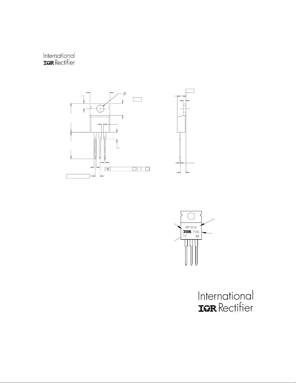
TO-220AB Package Outline
LO T CO D E 1789
A SSEMBLED ON WW 19, 1997
IN THE ASSEMBLY LINE "C"
INTERNATIONAL
REC TIFIER
LOGO
ASSEMBLY
LOT C OD E
PART NUMBER
DA TE CODE
YEA R 7 = 19 97
WEE K 19
LINE C
EX AMPLE: TH IS I S AN I R F1010
Dimensions are shown in millimeters (inches)
2.87 (.113)
2.62 (.103)
15.24 (.600)
14.84 (.584)
14.09 (.555)
13.47 (.530)
10.54 (.415)
10.29 (.405)
1 2 3
4
6.47 (.255)
6.10 (.240)
1.15 (.045)
MIN
4.06 (.160)
3.55 (.140)
3.78 (.149)
3.54 (.139)
- A -
4.69 (.185)
4.20 (.165)
- B -
1.32 (.052)
1.22 (.048)
IRF1407
LEAD ASSIGNMENTS
1 - GATE
2 - DRAIN
3 - SOUR C E
4 - DRAIN
0.93 (.037)
3X
1.40 (.055)
3X
1.15 (.045)
2.54 (.100)
NOTES:
1 DIMENSIONING & TOLERANCING PER ANSI Y14.5M, 1982. 3 OUTLINE CONFORMS TO JED EC OUTLINE TO-220AB.
2 CONTROLLIN G DIMENS ION : IN C H 4 HEATSINK & LE AD M E AS UREM EN T S DO NOT INCLUDE BURRS.
2X
0.69 (.027)
0.36 (.014 ) M B A M
0.55 (.022)
3X
0.46 (.018)
2.92 (.115)
2.64 (.104)
TO-220AB Part Marking Information
Data and specifications subject to change without notice.
This product has been designed and qualified for the Automotive [Q101] market.
Qualification Standards can be found on IR’s Web site.
IR WORLD HEADQUARTERS: 233 Kansas St., El Segundo, California 90245, USA Tel: (310) 252-7105
www.irf.com 9
TAC Fax: (310) 252-7903
Visit us at www.irf.com for sales contact information.10/01
 Loading...