

Page 1
Data Sheet No. PD-6.067B
)
Next Data SheetIndex
Previous Datasheet
To Order
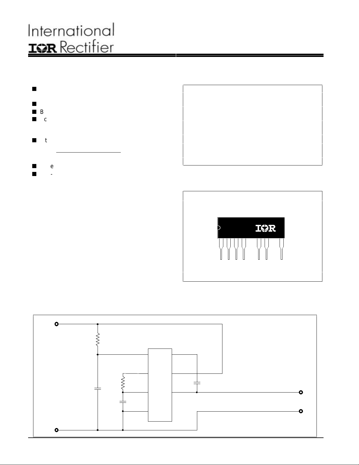
IR51HD320
SELF-OSCILLATING HALF-BRIDGE
Features
Output Power MOSFETs in half-bridge configuration
n
400V Rated Breakdown Voltage
High side gate drive designed for bootstrap operation
n
Bootstrap diode integrated into package
n
Accurate timing control for both Power MOSFETs
n
Matched delay to get 50% duty cycle
Matched deadtime of 1.2us
Internal oscillator with programmable frequency
n
f =
14 R 75 C
. × ( ) × Ω
Zener clamped Vcc for offline operation
n
Half-bridge output is out of phase with R
n
1
TT
+
T
Description
The IR51HD320 is a high voltage, high speed, selfoscillating half-bridge. Proprietary HVIC and latch
immune CMOS technologies, along with the
HEXFET® power MOSFET technology, enable
ruggedized single package construction. The front-end
features a programmable oscillator which functions
similar to the CMOS 555 timer. The supply to the
control circuit has a zener clamp to simplify offline
operation. The output features two HEXFETs in a
half-bridge configuration with an internally set
deadtime designed for minimum cross-conduction in
the half-bridge. Propagation delays for the high and
low side power MOSFETs are matched to simplify use
in 50% duty cycle applications. The device can
operate up to 400 volts.
Product Summary
V
(max) 400V
IN
Duty Cycle 50%
Deadtime 1.2µs
R
DS(on
PD (TA = 25 ºC) 2.0W
Package
IR51HD320
9506
1.8ΩΩ
Typical Connection
UP TO 400V DC BUS
V
IN
COM
RT
CT
IR 51HD 320
1
V
CC
2
R
T
3
C
T
4
COM
6
V
B
9
V
IN
7
VO
TO LO A D
Page 2
IR51HD320
Min.
-0.3
-0.3
-0.3
-0.3
-0.3
---
-5
---
---
---
-55
-55
---
Min.
VO + 10
---
-5
---
---
---
-40
Next Data SheetIndex
Previous Datasheet
To Order
Absolute Maximum Ratings
Absolute Maximum Ratings indicate sustained limits beyond which damage to the device may occur. All
voltage parameters are absolute voltages referenced to COM, all currents are defined positive into any lead.
The Thermal Resistance and Power Dissipation ratings are measured under board mounted and still air
conditions.
Parameter
Symbol Definition
V
IN
V
B
VO Half-Bridge Output Voltage
V
RT
V
CT
I
CC
I
RT
dv/dt Peak Diode Recovery dv/dt
P
D
R
θJA
T
J
T
S
T
L
High Voltage Supply
High Side Floating Supply Absolute Voltage
RT Voltage
CT Voltage
Supply Current (Note 1)
RT Output Current
Package Power Dissipation @ TA ≤ +25ºC
Thermal Resistance, Junction to Ambient
Junction Temperature
Storage Temperature
Lead Temperature (Soldering, 10 seconds)
Max. Units
400
425
VIN + 0.3 V
VCC + 0.3
VCC + 0.3
25 mA
5
4.0 V/ns
2.00 W
60 ºC/W
150
150 ºC
300
Recommended Operating Conditions
The Input/Output logic timing diagram is shown in Figure 1. For proper operation the device should be used
within the recommended conditions.
Parameter
Symbol Definition
V
B
V
IN
VO Half-Bridge Output Voltage
I
D
I
CC
T
A
Note 1: Because of the IR51HD320's application specificity toward off-line supply systems, this IC contains a
High Side Floating Supply Absolute Voltage
High Voltage Supply
Continuous Drain Current
(T
= 25ºC)
A
(TA = 85ºC)
Supply Current (Note 1)
Ambient Temperature
zener clamp structure between the chip V
and COM which has a nominal breakdown voltage of
CC
15.6V. Therefore, the IC supply voltage is normally derived by current feeding the V
(typically by means of a high value resistor connected between the chip V
voltage and a local decoupling capacitor from V
to COM) and allowing the internal zener clamp
CC
circuit to determine the nominal supply voltage. Therefore, this circuit should not be driven by a DC,
low impedance power source of greater than V
CLAMP
.
Max. Units
VO + V
CC
CLAMP
400 V
400
0.9 A
0.6
5mA
125 ºC
CC
and the rectified line
lead
Page 3

Dynamic Electrical Characteristics
TA = 25ºC
Typ.
270
g
1.4
1.2
50
Units
g
V
g
µA
V
µA
kHz
µA
mV
V
)
Ω
V
To Order
Next Data SheetIndex
Previous Datasheet
V
(VCC, VB) = 12V unless otherwise specified.
BIAS
Parameter
Symbol Definition Min.
t
rr Reverse Recovery Time (MOSFET Body Diode) ---
Q
rr Reverse Recovery Char
DT Deadtime, LS Turn-Off to HS Turn-On &
HS Turn-Off to LS Turn-On
DR
Duty Cycle ---
T
e (MOSFET Body Diode) ---
---
Static Electrical Characteristics
V
(VCC, VB) = 12V unless otherwise specified.
BIAS
Parameter TA = 25ºC
Symbol Definition Min. Typ. Max.
Supply Characteristics
+
V
CCUV
VCC Supply Undervoltage Positive Goin
Threshold
-
V
CCUV
VCC Supply Undervoltage Negative Goin
Threshold
I
QCC
V
CLAMPVCC
Quiescent VCC Supply Current --- 300 ---
Zener Shunt Clamp Voltage --- 15.6 ---
Floating Supply Characteristics
I
QBS
I
OS
Quiescent VBS Supply Current --- 30 --Offset Supply Leakage Current--- --- 50 V
Oscillator I/O Characteristics
f
OSC
I
CT
V
V
V
V
V
V
CTUV
RT
RT
RTUV
CT
CT
Oscillator Frequency --- 20 ---
CT Input Current --- 0.001 1.0
CT Undervoltage Lockout --- 100 --- 2.5V < V
+
RT High Level Output Voltage, VCC - R
-
RT Low Level Output Voltage ---20--- IRT = 100 µA
RT Undervoltage Lockout, VCC - R
+
2/3 VCC Threshold --- 8.0 ---
-
1/3 VCC Threshold --- 4.0 ---
Output Characteristics
R
V
DS(on
SD
Static Drain-to-Source On-Resistance --- 1.8 --Diode Forward Voltage --- 0.7 ---
T
T
--- 8.4 ---
--- 8.0 ---
--- 100 ---
---20--- IRT = -100 µA
--- 200 ---
--- 200 --- IRT = 1 mA
--- 100 --- 2.5V < VCC < V
IR51HD320
Max. Units Test Conditions
--- ns IF = 900mA
--- µC di/dt = 100A/µs
--- µs
--- % f
Test Conditions
= 20 kHz
OSC
ICC = 5 mA
= VIN = 400V
B
RT = 35.7 kΩ,
= 1 nF
C
T
R
= 7.04 kΩ,
T
= 1 nF
C
T
< V
CC
CCUV
IRT = -1 mA
CCUV
ID = 900 mA
Tj = 150 ºC
+
+
Page 4

IR51HD320
7
g
g
To Order
Next Data SheetIndex
Previous Datasheet
Functional Block Diagram
V
B
6
1
V
CC
2
R
T
3
C
T
IR2151 VO
IRFC320
IRFC320
Lead Definitions
Lead
Symbol Description
V
CC
R
T
C
T
Logic and internal gate drive supply voltage. An internal zener clamp diode at 15.6 V nominal is
included to allow the Vcc to be current fed directly from V
resistor.
Oscillator timing resistor input; a resistor is connected from RT to CT. RT is out of phase with
the half-brid
e output (VO).
Oscillator timing capacitor output; a capacitor is connected from CT to COM in order to program
the oscillator frequency accordin
to the following equation:
f =
14 R 75 C
. × ( ) × Ω
1
TT
+
+
V
9
4
COM
typically by means of a high value
IN
where 75Ω is the effective impedance of the R
V
B
High side gate drive floating supply. For bootstrap operation a high voltage fast recovery diode is
needed to feed from V
V
IN
High voltage supply.
VO Half-bridge output.
COM Logic and low side of half-bridge return.
output stage.
T
to VB.
CC
Page 5

Lead Assignments
B
6
R
T
50%
To Order
Next Data SheetIndex
Previous Datasheet
IR51HD320
V
VO
CC
97
V
IN
V
R C COM V
CC
TT
9 Lead SIP w/o Leads 5 & 8
4321
V0
IR51HD320
V
+
CCUV
R
T
C
T
V
CLAMP
50%
90%
HIGH
SIDE
+
V
LOW
10%
DT
90%
SIDE
0
10%
Figure 1. Input/Output Timing Diagram Figure 2. Deadtime Waveform Definitions
Page 6

IR51HD320
To Order
Next Data SheetIndex
Previous Datasheet
Package Outline
WORLD HEADQUARTERS: 233 Kansas St., El Segundo, California 90245, Tel: (310) 322 3331
EUROPEAN HEADQUARTERS: Hurst Green, Oxted, Surrey RH8 9BB, UK Tel: ++ 44 1883 732020
IR CANADA: 7321 Victoria Park Ave., Suite 201, Markham, Ontario L3R 2Z8, Tel: (905) 475 1897
IR GERMANY: Saalburgstrasse 157, 61350 Bad Homburg Tel: ++ 49 6172 96590
IR ITALY: Via Liguria 49, 10071 Borgaro, Torino Tel: ++ 39 11 451 0111
IR FAR EAST: 171 (K&H Bldg.), 30-4 Nishi-ikebukuro 3-Chome, Toshima-ku, Tokyo Japan Tel: 81 3 3983 0086
IR SOUTHEAST ASIA: 315 Outram Road, #10-02 Tan Boon Liat Building, Singapore 0316 Tel: 65 221 8371
http://www.irf.com
Sales Offices, Agents and Distributors in Major Cities Throughout the World. Data and specifications subject to change without notice.
© 1996 International Rectifier Printed in U.S.A. 3-96
 Loading...