

Page 1
IR3651SPbF
10/11/2006
HIGH VOLTAGE SYNCHRONOUS PWM BUCK CONTROLLER
Description
The IR3651 is a high voltage PWM controller
designed for high performance synchronous Buck
DC/DC applications. The IR3651 drives a pair of
external N-MOSFETs using a programmable
switching frequency up to 400kHz allows flexibility
to tune the operation of the IC to meet system
level requirements, and synchronization allows
the simplification of system level filter design. The
output voltage can be precisely regulated using
the internal 1.25V reference voltage for low
voltage applications. Protection such as under
voltage lockout and hiccup current limit are
provided to give required system level security in
the event of fault conditions.
Features
• High Voltage Operating up to 75V
• Programmable Switching Frequency up to 400kHz
• 1A Output Drive Capability
• Precision Reference Voltage (1.25V)
• Programmable Soft-Start
• Programmable Over Current Protection
• Hiccup Current Limit Using MOSFET R
DS(on)
sensing
• External Frequency Synchronization
• 14-pin SOIC Package
Applications
• 48V non-isolated DC to DC Converter
• Embedded Telecom Systems
• Networking and Computing Voltage Regulator
• Distributed Point of Load Power Architectures
• General high voltage DC/DC Converters
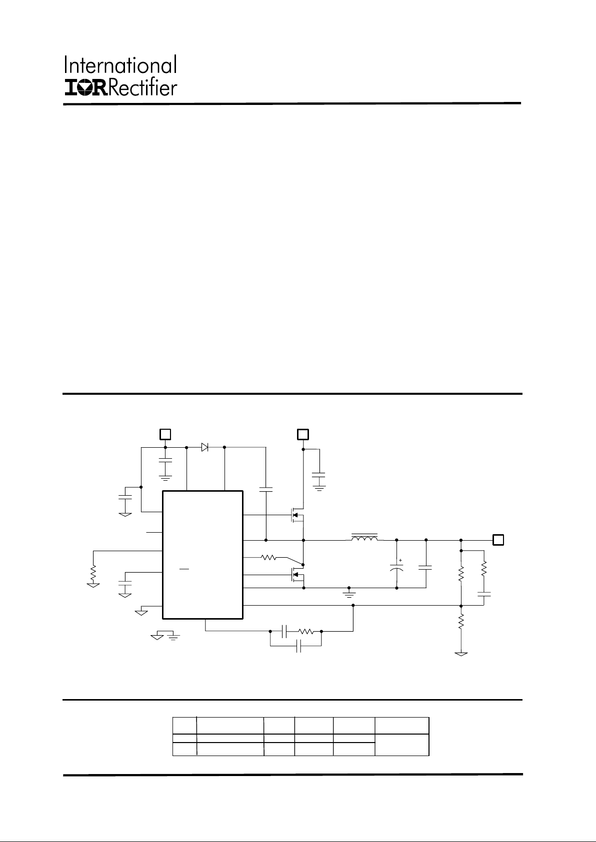
Typical application Circuit
ORDERING INFORMATION
PKG PACKAGE PIN PARTS PARTS T&R
DESIG DESCRIPTION COUNT PER TUBE PER REEL ORIANTAION
S IR3651SPBF 14 55 ------S IR3651STRPBF 14 -------- 2500
Fig A
R
OCset
IR3651S
Vcc
Vb
HDrv
LDrv
Fb
Gnd
Comp
SS/SD
C2
C3
C7
R4
Q1
Q2
L1
Vout
C8
V
aux
=12V
PGnd
SYNC
Vin: 12V-75V
DRVcc
C1
R1
R2
Vs
C4
C6
Rt
R5
C5
C10
C9
R3
OCset
Data Sheet No.PD94720
Page 2
IR3651SPbF
10/11/2006
ABSOLUTE MAXIMUM RATINGS
(Voltages referenced to GND)
• Vcc, DRVcc Supply Voltage ..................................… -0.3V to 20V
• Vs Supply Voltage …………………………………….. -0.3V to 150V
• Vb Supply Voltage …………………………………….. -0.3V to Vs+20V
• OCset …………….…………………………………….. 10mA
• Storage Temperature Range ..................................... -65°C To 150°C
• Operating Junction Temperature Range ................... -40°C To 150°C
• ESD Classification …………………………………..… JEDEC, JESD22-A114 (1K)
• Moisture Sensitivity Level ……………………………. JEDEC Level 3 @ 260
o
C
CAUTION:
Stresses beyond those listed under “Absolute Maximum Ratings” may cause permanent damage to
the device. These are stress ratings only and functional operation of the device at these or any other conditions
beyond those indicated in the operational sections of the specifications are not implied.
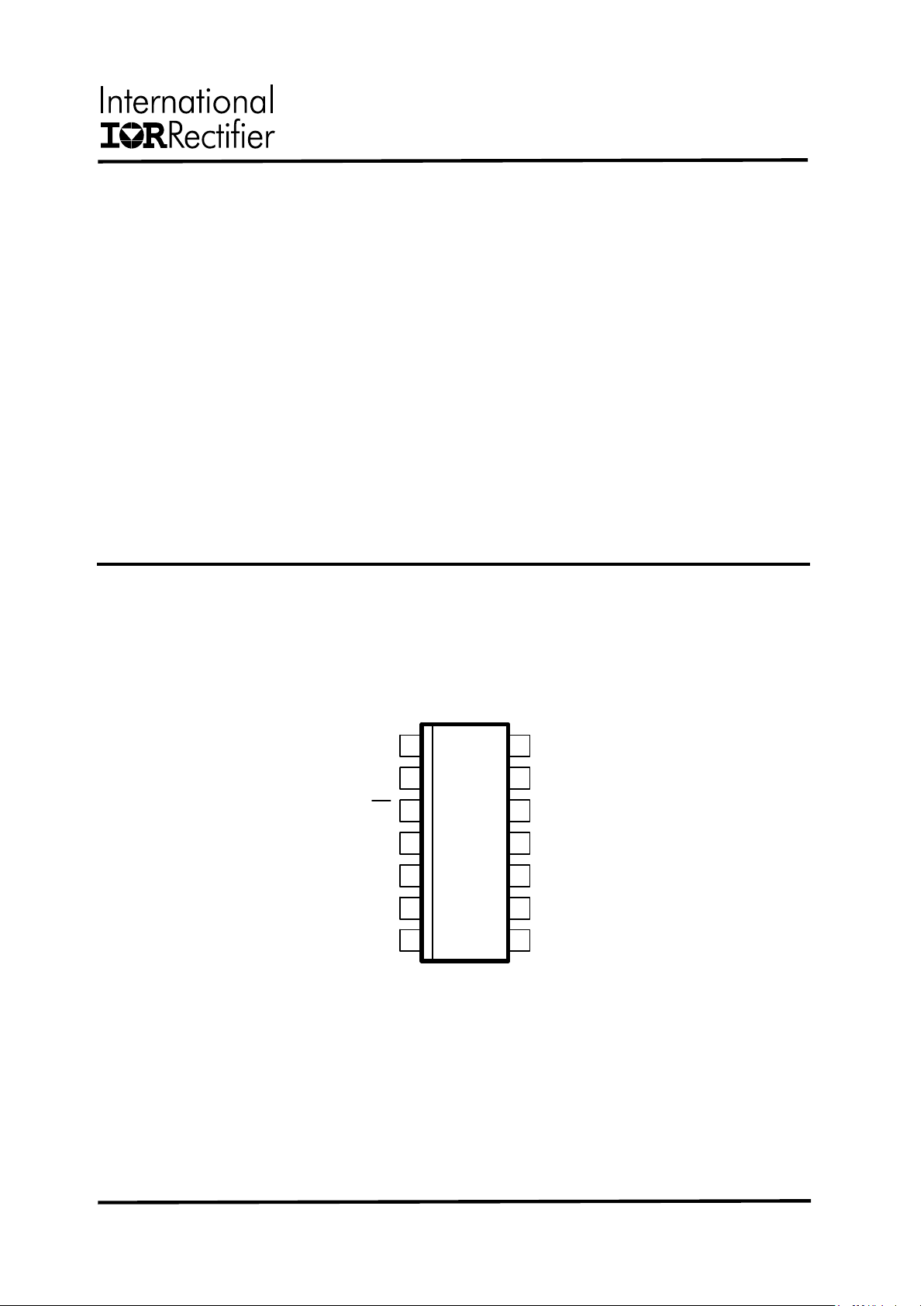
Package Information
14-Pin SOIC NB (S)
2
Θ
JA
= 88.2o C/W
ΘJC= 37o C/W
SYNC
Fb
Vcc
Ldrv
DRVcc
OCset
HDrv
Vs
7
6
5
4
8
9
10
11
3
2
1
12
Rt
13
14
Gnd
PGnd
SS/SD
Comp
Vb
Page 3
IR3651SPbF
10/11/2006
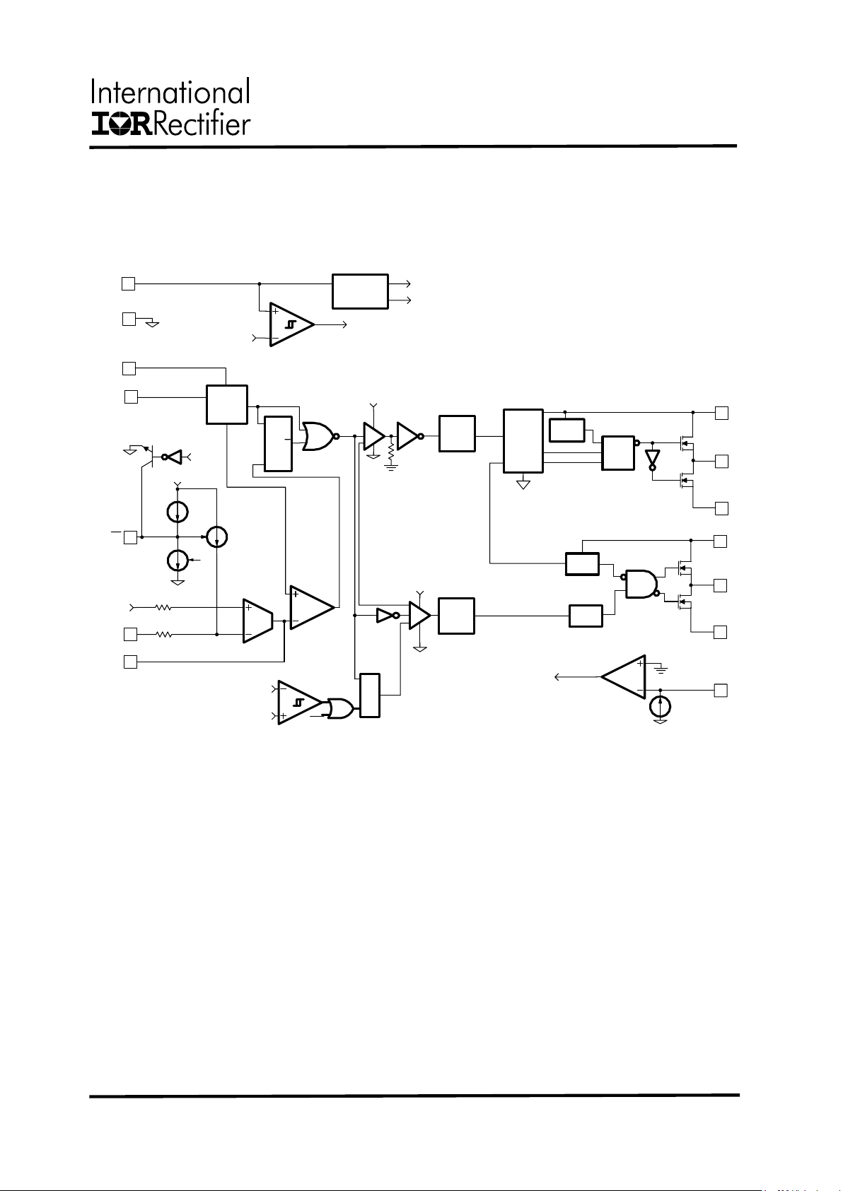
Block Diagram
Fig. 1: Simplified block diagram of the IR3651
3
64uA Max
POR
Oscillator
Error Amp
Ct
Error Com p
Reset Dom
Vcc
Gnd
4.17V
0.25V
Bias
Generator
3V
1.25V
POR
SS/SD
Fb
Comp
25K
25K
3V
R
S
Q
SYNC
Vb
Rt
4
3
1
2
8
11
13
Vcc
DELAY
UV
DETECT
UV Q
S
R
UV
DETECT
HIGH
VOLTAGE
LEVEL
SHIFT
CIRCUIT
LOW
VOLTAGE
LEVEL
SHIFT
LOW
VOLTAGE
LEVEL
SHIFT
HDrv9
Vs
10
DRVcc7
LDrv6
PGND
5
Vcc
1.25V
14
Rt
10uA
OCset
12
OCP
3uA
OCP
20uA
0.3V
SS
Q
R
S
POR
PBias
Page 4

IR3651SPbF
10/11/2006
Pin Description
Pin Name Description
1 Fb Inverting input to the error amplifier. This pin is connected directly to the
output of the regulator via resistor divider to set the output voltage and
provide feedback to the error amplifier.
2 Comp Output of error amplifier. An external resistor and capacitor network is
typically connected from this pin to ground to provide loop compensation.
3 SS/SD Soft start / shutdown. This pin provides user programmable soft-start
function. Connect an external capacitor from this pin to ground to set the
start up time of the output voltage. The converter can be shutdown by
pulling this pin below 0.3V.
4 SYNC The internal oscillator can be synchronized to an external clock via this
pin.
5 PGnd Power Ground. This pin serves as a separate ground for the MOSFET
driver and should be connected to the system’s power ground plane.
6 LDrv Output driver for low side MOSFET.
7 DRVcc This pin provides biasing for the internal low side driver. A minimum of
0.1uF, high frequency capacitor must be connected from this pin to power
ground.
8 Vb This pin powers the high side driver and must be connected to a voltage
higher than bus voltage. A minimum of 0.1uF, high frequency capacitor
must be connected from this pin to switch node.
9 HDrv Output driver for high side MOSFET
10 Vs Switch node. Connect this pin to the source of the upper MOSFET and
the drain of the lower MOSFET. This pin is return path for the upper gate
driver.
11 Vcc This pin provides power for the internal blocks of the IC. A minimum of
0.1uF, high frequency capacitor must be connected from this pin to
ground.
12 OCSet Current limit set point. A resistor from this pin to drain of low side
MOSFET will set the current limit threshold.
13 Gnd Signal ground for internal reference and control circuitry.
14 Rt Connecting a resistor from this pin to ground sets the oscillator frequency.
4
Page 5
IR3651SPbF
10/11/2006
Recommended Operating Conditions
Parameter SYM Test Condition Min TYP MAX Unit
s
Reference Voltage
Feedback Voltage VFB 1.25 V
0oC<Tj<125oC -1.5 +1.5 % Accuracy
-40
o
C<Tj<125oC,
Note1
-3 +1.5 %
Fb Voltage Line Regulation LREG 5V<Vcc<12V 2.0 mV
Supply Current
VCC Supply Current (Stat)
I
CC(Static)
SS=0V, No Switching 6 7 mA
VCC Supply Current (Dyn) I
CC(Dynamic)
Fs=200kHz, C
LOAD
=1.5nF 6 7 mA
DRVcc Supply Current (Stat) I
C(Static)
SS=0V, No Switching 0.3 0.5 mA
DRVcc Supply Current (Dyn) I
C(Dynamic)
Fs=200kHz, C
LOAD
=1.5nF 4 5 mA
Vb Supply Current (Stat) I
b(Static)
SS=0V, No Switching 0.3 0.5 mA
Vb Supply Current (Dyn) I
b(Dynamic)
F
s
=200kHz, C
LOAD
=1.5nF 4.5 5.5 mA
Under Voltage Lockout
VCC-Start-Threshold
VCC_UVLO(R)
Supply ramping up 4.0 4.17 4.35 V
VCC-Stop-Threshold
VCC_UVLO(F)
Supply ramping down 3.75 4.1 V
VCC-Hysteresis
Supply ramping up and down 0.15 0.25 0.3 V
DRVcc-Start-Threshold
DRcc_UVLO(R)
Supply ramping up 8.3 9 9.7 V
DRVcc-Stop-Threshold
DRVcc_UVLO(F)
Supply ramping down 7.5 8.2 8.9 V
DRVCc-Hysteresis
Supply ramping up and down 0.6 0.9 V
Vb-Start-Threshold
Vb_UVLO(R)
Supply ramping up 8.3 9 9.7 V
Vb-Stop-Threshold
Vb_UVLO(F)
Supply ramping down 7.5 8.2 8.9 V
Vb-Hysteresis Supply ramping up and down 0.6 0.9 V
Oscillator
Frequency FS Rt=120K
Rt=51K
170
340
200
400
230
460
kHz
Ramp Amplitude V
ramp
Note2
1.25 V
Min Duty Cycle D
min
Fb=2V 0 %
Min Pulse Width D
min(ctrl)
F
s
=200kHz, Note2
200 ns
Max Duty Cycle D
max
F
s
=200kHz, Fb=1.2V
F
s
=400kHz, Fb=1.2V
80
70
%
Sync Frequency Range Sync(Fs) 20% above free running freq 480 kHz
Sync Pulse Duratin Sync(puls) 200 ns
Sync high Level T hr es hold Sync(H) 2 V
Sync Low Level T hreshold S ync(L) 0.8 V
Electrical Specifications
Unless otherwise specified, these specifications apply over Vcc=5V; DRVcc=Vb=12V, 0oC<Tj< 125oC
5
Symbol Definition Min Max Units
V
bus
Converting Voltage 12 75 V
Vcc Supply Voltage 4.5 13.2 V
DRVcc Supply Voltage 10 16 V
Vb to Vs Supply Voltage 10 16 V
Fs Operating Frequency 100 400 kHz
Tj Junction Temperature -40 125 oC
Page 6
IR3651SPbF
10/11/2006
Parameter SYM Test Condition Min TYP MAX Units
Error Amplifier
Input Bias Current IFB SS=3V, Fb=1V -0.1 -0.4
µA
Source/Sink Current I(source/Sink) 50 85 120
µA
Transconductance gm 1500 2400 3000
µmho
Soft Start/SD
Soft Start Current ISS SS=0V 15 20 25
µA
Shutdown Output
Threshold
SD 0.25 V
Over Current Protection
OCSET Current I
OCSET
7.5 10 12.5
µA
Hiccup Current I
Hiccup
Note2
3
µA
Hiccup Duty Cycle Hiccup(duty)
I
Hiccup
/ I
SS
, Note2
5 %
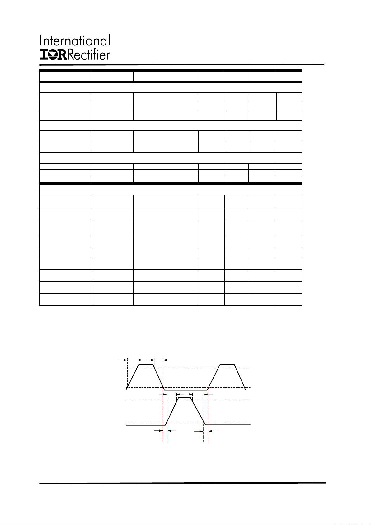
Output Drivers
LO, Drive Rise Time Tr(Lo) CL=1.5nF
See Fig 2, Note2
10 20 ns
HI Drive Rise Time Tr(Hi) CL=1.5nF,
See Fig 2, Note2
10 20 ns
LO Drive Fall Time Tf(Lo) CL=1.5nF
See Fig 2,Note2
10 20 ns
HI Drive Fall Time Tf(Hi) CL=1.5nF,
See Fig 2,Note2
10 20 ns
Dead Band Time Tdead See Fig 2 30 45 100 ns
Upper Driver Source
Current
I
upper(source)
HDrv short circuit pulsed
current. PW<10us
1.0 A
Upper Driver Sink
Curret
I
upper(sink)
HDrv short circuit pulsed
current. PW<10us
1.0 A
Lower Driver Source
Current
I
lower(source)
LDrv short circuit pulsed
current. PW<10us
1.0 A
Lower Driver Sink
Current
I
lower(sink)
LDrv short circuit pulsed
current. PW<10us
1.0 A
9V
2V
9V
2V
High Side Driver
(HDrv)
Low Side Driver
(LDrv)
Tr
Tf
Deadband
H_to_L
Deadband
L_to_H
Tr
Tf
Fig. 2: Definition of Rise/Fall time and Deadband Time
6
Note1: Cold temperature performance is guaranteed via correlation using statistical quality control. Not tested in production.
Note2: Guaranteed by Design but not tested in production.
Page 7

IR3651SPbF
10/11/2006
7
TYPICAL OPERATING CHRACTERISTICS (-40oC TO +125oC)
Vfb
1.235
1.237
1.239
1.241
1.243
1.245
1.247
1.249
1.251
1.253
-40 -30 -20 -10 0 10 20 30 40 50 60 70 80 90 100 110 120 130
Temp [C]
[V]
Icc(dynamic)
4.5
4.8
5.1
5.4
5.7
6
6.3
6.6
-40-30-20-10 0 10 203040 5060 708090100110120130
Temp [C]
[mA]
Ic(dynamic)
3.5
3.58
3.66
3.74
3.82
3.9
3.98
4.06
-40-30-20-10 0102030405060708090100110120130
Temp [C]
[mA ]
Ib(dynamic)
4.6
4.65
4.7
4.75
4.8
4.85
4.9
4.95
-40 -30 -20 -10 0 10 20 30 40 50 60 70 80 90 100 110 120 130
Temp [C]
[mA]
Icc(static)
4.5
4.8
5.1
5.4
5.7
6
6.3
6.6
-40 -30 -20 -10 0 10 20 30 40 50 60 70 80 90 100 110 120 130
Temp [C]
[mA]
Transconductance
1.6
1.6 8
1.7 6
1.8 4
1.9 2
2
2.08
2.16
-40-30-20-10 0 102030405060708090100110120130
Temp [ C]
[mM HO]
DRVcc_UVLO
8.85
8.9
8.95
9
9.05
9.1
9.15
9.2
-40-30-20-100 102030405060708090100110120130
Temp [ C]
[V]
Vb_UVLO
8.8
8.85
8.9
8.95
9
9.05
9.1
9.15
9.2
-40-30-20-100 102030405060708090100110120130
Temp [C]
[V]
Page 8

IR3651SPbF
10/11/2006
8
TYPICAL OPERATING CHRACTERISTICS (-40oC TO +125oC)
Frequency RT=120K
199
199.5
200
200.5
201
201.5
-40 -30 -20 -10 0 10 20 30 40 50 60 70 80 90 100 110 120 130
Temp [C]
[
kHz
]
Dead time
20
30
40
50
60
70
80
90
10 0
-40-30-20-10 0 10203040 5060 708090100110120130
Temp [C]
[ns]
Max DC @ 200KHz
88
88.5
89
89.5
90
90.5
91
-40-30-20-100 102030405060708090100110120130
Temp [C ]
[% ]
Vcc_UVLO
4.1
4.12
4.14
4.16
4.18
4.2
4.22
4.24
4.26
4.28
4.3
-40-30-20-100 102030405060708090100110120130
Temp [ C]
[V]
Iss
-25.000
-24.000
-23.000
-22.000
-21.000
-20.000
-19.000
-18.000
-17.000
-16.000
-15.000
-50-30-101030507090110130
Temp [C]
[uA]
Iocset
-13.000
-12.500
-12.000
-11.500
-11.000
-10.500
-10.000
-9.500
-9.000
-8.500
-8.000
-50 -30 -10 10 30 50 70 90 110 130
Temp [C]
[uA]
Page 9

IR3651SPbF
10/11/2006
Circuit Description
9
THEORY OF OPERATION
Introduction
The IR3651 is a voltage mode PWM
synchronous controller. The output voltage is se t
by feedback pin (Fb) and the internal reference
voltage (1.25V). These are two inputs to error
amplifier. The error signal between these two
inputs is compared to a fixed frequency linear
sawtooth ramp and generates fixed frequency
pulses of variable duty-cycle (D) which drivers Nchannel external MOSFETs.
The timing of the IC is controlled by an internal
oscillator circuit that can be externally
programmed up to 400kHz.
The IR3651 operates with a wide input voltage
from 36V to 75V allowing an extended operating
input voltage range.
The current limit is programmable and uses onresistance of the low-side MOSFET, eliminating
the need for an external current sense resistor
.
Under-Voltage Lockout
The under-voltage lockout circuit monitors the
Vcc supply and assures that the IC doesn’t starts
until the Vcc reaches the set threshold. Lockout
occurs if Vcc falls below 4.1V. Normal operation
resumes once Vcc rises above the set value.
Shutdown
The output can be shutdown by pulling the softstart pin below 0.3V. This can be easily done by
using an external small signal transistor. During
shutdown both MOSFET drivers will be turned
off. Normal operation will resume by cycling soft
start pin.
Error Amplifier
The IR3651 is a voltage mode controller. The
error amplifier is of transconductance type. The
amplifier is capable of operating with Type III
compensation control scheme using low ESR
output capacitance.
Operating Frequency Selection
The switching frequency is determined by
connecting an external resistor (Rt) to ground.
Figure 3 provides a graph of oscillator frequency
versus Rt.
Frequency Synchronization
The IR3651 is capable of accepting an external
digital synchronization signal. Synchronization
will be enabled by the ris ing edge at an externa l
clock. Switching frequency is set by external
resistor (Rt). During synchronization, Rt is
selected such that the free running frequency is
20% below the synchronization frequency.
When unused, the sync pin will remain floating
and is noise immune.
Pre-Bias Startup
IR3651 is able to start up into pre-charged
output, which prevents oscillation and
disturbances of the output voltage.
The output starts in asynchronous fashion and
keeps the synchronous MOSFET off until the
first gate signal for control MOSFET is
generated. Below figure shows a typical PreBias condition at start up.
Depends on system configuration, specific
amount of output capacitors may be required to
prevent discharging the output voltage
Fig. 3: Switching Frequency vs. Rt
Switching Frequency vs. Rt
0
50
100
150
200
250
300
350
400
450
0 50 100 150 200 250 300
Rt (Kohm)
Switching Frequency (kHz)
Vo
Time
Volt
Pre-Bias Voltage
(Output Voltage before startup)
Page 10

IR3651SPbF
10/11/2006
Soft-Start
The IR3651 has programmable soft-start to
control the output voltage rise and limit the inrush
current during start-up.
To ensure correct start-up, the soft-start
sequence initiates when Vcc rises above its
threshold and generate the Power On Ready
(POR) signal. The soft-start function operates by
sourcing current to charge an external capacitor
to about 3V.
Initially, the soft- start function clamps the output
of error amplifier by injecting a current (64uA)
into the Fb pin and generates a voltage about
1.6V (64ux25K) across the negative input of error
amplifier (see figure 4).
The magnitude of the injected current is inverse l y
proportional to the voltage at the soft-start pin. As
the soft-start voltage ramps up, the injected
current decreases linearly and so does the
voltage at negative input of error amplifier.
When the soft-start capacitor is around 1V, the
voltage at the positive input of the erro r amplifier
is approximately 1.25V.
The output of error amplifier will start increasing
and generating the first PWM signal. As the softstart capacitor voltage continues to go up, the
current flowing into the Fb pin will keep
decreasing.
The feedback voltage increases linearly as the
soft start voltage ramps up. When soft-start
voltage is around 2V the output voltage is
reached the steady state and the injected current
is zero.
Figure 5 shows the theoretical operational
waveforms during soft-start.
The output voltage start-up time is the time
period when soft-start capacitor voltage
increases from 1V to 2V.
The start-up time will be dependent on the size of
the external soft-start capacitor and can be
estimate by:
Fig. 4: Soft-Start circuit for IR3651
Fig. 5: Theoretical operation waveforms
during soft-start
20uA
64uA
POR
Error Am p
SS/SD
Fb
Comp
25K
1.25V
25K
3V
Soft-Sta rt
Voltage
Voltage at negative input
of Error Amp
Voltage at Fb pin
Current flowing
into Fb p in
64uA
0uA
0V
1.25V
≅
1.6V
1.25V
0V
3V
≅
2V
≅
1V
Output of UVLO
POR
For a given start-up time, the soft-start capacitor
(nF) can be estimated as:
V1V2
C
T
µA20
ss
start
−=∗
)1 --(msTA20C
startSS
)(*
µ
≅
10
Page 11

IR3651SPbF
10/11/2006
Over-Current Protection
The over current protection is performed by
sensing current through the R
DS(on)
of low side
MOSFET. This method enhances the converter’s
efficiency and reduce cost by eliminating a
current sense resistor. As shown in figure 6, an
external resistor (R
SET
) is connected between
OCSet pin and the drain of low side MOSFET
(Q2) which sets the current limit set point.
The internal current source develops a voltage
across R
SET
. When the low side MOSFET is
turned on, the inductor current flows through the
Q2 and results a voltage which is given by:
The OCP circuit starts sampling current
approximately 200ns before the low gate drive
turns off. The OCSet pin is internally clamped
during deadtime to prevent false trigging, figure 8
shows the OCSet pin during one switching cycle.
Fig. 6: Connection of over current sensing resistor
Fig. 7: 3uA current source for discharging
soft-start capacitor during hiccup
An over current is detected if the OCSet p in goes
below ground. This trips the OCP comparator
and cycles the soft start function in hiccup mode.
The hiccup is performed by charging and
discharging the soft-start capacitor in certain
slope rate. As shown in figure 7 a 3uA current
source is used to discharge the soft-start
capacitor.
The OCP comparator resets after every soft start
cycles, the converter stays in this mode until the
overload or short circuit is removed. The
converter will automatically recover.
SS1 / SD
20
28uA
3uA
OCP
)2) --(I(R)R(IV
LDS(on)OCSetOCSetOCSet
∗−∗=
0)I(R)R(IV
LDS(on)OCSetOCSetOCSet
=∗
−
∗=
)3 --(
R
IR
II
onDS
OCSetOCSet
criticalLSET
)(
)(
∗
==
Fig. 8: OCset pin during normal condition
Ch1: Inductor point, Ch2:Ldrv, Ch3:OCSet
The value of R
SET
should be checked in an actual
circuit to ensure that the over current protection
circuit activates as e xpected. The IR3651 current
limit is designed primarily as disaster preventing,
"no blow up" circuit, and doesn't operate as a
precision current regulator.
The critical inductor current can be ca lculated by
setting:
20uA
L1
R
SET
IR3651
OCSet
I
OCSET
V
OUT
Hiccup
Control
Q1
Q2
2
i
I51II
L
ocriticalLSET
∆
+== *.
)(
11
Page 12

IR3651SPbF
10/11/2006
Application Information
Output Voltage Programming
Output voltage is programmed by reference
voltage and external voltage divider. The Fb pin
is the inverting input of the error amplifier , which
is internally referenced to 1.25V. The divider is
ratioed to provide 1.25V at the Fb p in when the
output is at its desired value. The output voltage
is defined by using the following equation:
When an external resistor divider is connected to
the output as shown in figure 9.
Equation (4) can be rewritten as:
For the calculated values of R
8
and R9see
feedback compensation section.
)4 --(
R
R
1VV
9
8
refo
⎟
⎟
⎠
⎞
⎜
⎜
⎝
⎛
+∗=
Fig. 9: Typical application of the IR3651 for
programming the output voltage
)5 --(
VV
V
RR
refO
ref
89
⎟
⎟
⎠
⎞
⎜
⎜
⎝
⎛
−
∗=
Soft-Start Programming
The soft-start timing can be programmed by
selecting the soft-start capacitance value. The
start-up time of the converter can be calculated
by using:
Where T
start
is the desired start-up time (ms)
For a start-up time of 5ms, the soft-start
capacitor will be 0.1uF. Choose a ceramic
capacitor at 0.1uF.
)1 --(TA20C
startSS
*
µ
≅
Fb
IR3651
V
OUT
R
9
R
8
12
Page 13

IR3651SPbF
10/11/2006
Input Capacitor Selection
The input filter capacitor should be selected
based on how much ripple the supply can
tolerate on the DC input line. The ripple current
generated during the on time of upper MOSFET
should be provided by input capacitor. T he RMS
value of this ripple is expre ssed by:
Where:
D is the Duty Cycle
I
RMS
is the RMS value of the input capacitor
current.
Io is the output current.
For applications with input supplies above 30V,
choice of input capacitor type is limited to
ceramics or aluminum electrolytics. Ceramic
capacitors offer high peak current capabilities,
they also feature low ESR and ESL at higher
frequency which enhance better efficiency,
however high voltage ceramic capacitors are
available with only in low value capacitance. A
combination of ceramic capacitors and
electrolytic capacitors are recommended .
Inductor Selection
The inductor is selected based on output power ,
operating frequency and efficiency requirements.
Low inductor value causes large ripple current,
resulting in the smaller size, faster response to a
load transient but poor efficiency and high output
noise. Generally, the selection of inductor value
can be reduced to desired maximum ripple
current in the inductor . The optimum point is
usually found between 20% and 50% ripple of
the output current.
For the buck converter, the inductor value for
desired operating ripple current can be
determined using the following relation:
Where:
)7 --(D1DII
oRMS
)( −∗∗=
in
o
V
V
D =
s
oin
F
1
Dt
t
i
LVV ∗=∗=−
∆
∆
∆
;
)( i
∆
()
)8 --(
FiV
V
VVL
sin
o
oin
*
∆
∗
∗−=
cycle DutyD
time on Turnt
frequency SwitchingF
current ripple Inductori
Voltage OutputV
voltage input MaximumV
s
o
in
=
=
=
=
=
=
∆
∆
Output Capacitor Selection
The voltage ripple and transient requirements
determine the output capacitors types and
values. The criteria is normally based on the
value of the Effective Series Resistance (ESR).
However the actual capacitance value and the
Equivalent Series Inductance (ESL) are other
contributing components, these components can
be described as:
Since the output capacitor has major role in
overall performance of converter and determines
the result of transient response, selection of
capacitor is critical. The IR3651 can perform we ll
with all types of capacitors.
As a rule the capacitor must have low enough
ESR to meet output ripple and load transient
requirements, yet have high enough ESR to
satisfy stability requirements.
The goal for this design is to meet the voltage
ripple requirement in smallest possible capacitor
size. Therefore ceramic capacitor is selec ted due
to low ESR and small size.
In the case of tantalum or low ESR electrolytic
capacitors, the ESR dominates the output
voltage ripple, equation (9) can be used to
calculate the required ESR for the specific
voltage ripple.
current ripple InductorI
ripple voltage OutputV
FC8
I
V
ESL
L
V
V
-(9)- ESRIV
VVVV
L
o
so
L
Co
in
ESLo
LESRo
CoESLoESRoo
=
=
=
⎟
⎠
⎞
⎜
⎝
⎛
=
=
++=
∆
∆
∆
∆
∆
∆∆
∆∆∆
∆
**
*
*
)(
)(
)(
)()()(
13
Page 14

IR3651SPbF
10/11/2006
Power MOSFET Selection
The IR3651 uses two N-Channel MOSFETs. The
selections criteria to meet power transfer
requirements is based on maximum drain-source
voltage (V
DSS
), gate-source drive voltage (Vgs),
maximum output current, On-resistance R
DS(on)
and thermal management.
The MOSFET must have a maximum operating
voltage (V
DSS
) exceeding the maximum input
voltage (V
in
).
The gate drive requirement is almost the same
for both MOSFETs. Logic-level transis tor can be
used and caution should be taken with devices at
very low V
gs
to prevent undesired turn-on of the
complementary MOSFET, which results in shootthrough current.
The total power dissipation for MOSFETs
includes conduction and switching losses. For
the Buck converter the average inductor cu rrent
is equal to the DC load current. The conduction
loss is defined as:
The R
DS(on)
temperature dependency should be
considered for the worst case operation . This is
typically given in the MOSFET data sheet.
Ensure that the conduction losses and switching
losses do not exceed the package ratings or
violate the overall thermal budget.
The switching loss is more difficult to calculate,
even though the switching transition is well
understood. The reason is the effect of the
parasitic components and switching times during
the switching procedures such as turn-on / turnoff delays and rise and fall times. The control
MOSFET contributes to the majority of the
dependency e temperatur R
D)(1RIswitch) (lowerP
DRIswitch) (upperP
ds(on)
ds(on)
2
loadcond
ds(on)
2
loadcond
=
∗−∗∗==
∗∗∗==
ϑ
ϑ
ϑ
switching losses in synchronous Buck converter.
The synchronous MOSFET turns on under zero
voltage conditions, therefore, the turn on losses
for synchronous MOSFET can be neglected.
With a linear approximation, the total switching
loss can be expressed as:
Where:
V
ds(off)
= Drain to source voltage at the off time
t
r
= Rise time
t
f
= Fall time
T = Switching period
I
load
= Load current
The switching time waveforms is shown in
figure10.
-(10)- I
T
tt
2
V
P
load
fr
offds
sw
**
)(
+
=
V
DS
V
GS
10%
90%
t
d
(ON)
t
d
(OFF)
t
r
t
f
Fig. 10: switching time waveforms
14
Page 15

IR3651SPbF
10/11/2006
Feedback Compensation
The IR3651 is a voltage mode controller; the
control loop is a single voltage feedback path
including error amplifier and error comparator. To
achieve fast transient response and accurate
output regulation, a compensation circuit is
necessary. The goal of the compensation
network is to provide a closed loop transfer
function with the highest 0dB crossing fr equency
and adequate phase margin (greater than 45
o
).
The output LC filter introduces a double pole, –
40dB/decade gain slope above its corner
resonant frequency, and a total phase lag of 180
o
(see figure 11). The resonant frequency of the LC
filter expressed as follows:
Figure 11 shows gain and phase of the LC filter.
Since we already have 180
o
phase shift just from
the output filter, t h e sy st e m risks b ei ng unstable.
The IR3651’s error amplifier is a d ifferential-input
transconductance amplifier. The output is
available for DC gain control or AC phase
compensation.
The error amplifier can be compensated either in
typeII or typeIII compensation. When it is used in
typeII compensation the transconductance
properties of the error amp lifier become evident
and can be used to cancel one of the output filter
poles. This will be accomplished with a series RC
circuit from Comp pin to ground as shown in
figure 12.
This method requires that the output capacitor
should have enough ESR to satisfy stability
requirements. In general the output capacitor’s
ESR generates a zero typically at 5kHz to 50kHz
which is essential for an acceptable phase
margin.
-(11
)
-
CL2
1
F
oo
LC
∗∗
=
π
Gain
F
LC
0dB
Phase
0
F
LC
-180
Frequency
Frequency
-40dB/decade
Fig. 11: Gain and Phase of LC filter
The ESR zero of the output capacitor is
expressed as follows:
The transfer function (Ve/Vo) is given by:
The (s) indicates that the transfer function varies
as a function of frequency. This configuration
introduces a gain and zero, expressed by:
The gain is determined by the voltage divider and
error amplifier’s transconductance gain.
First select the desired zero-c rossover frequency
(Fo):
Use the following equation to calculate R4:
Where:
V
in
= Maximum Input Voltage
V
osc
= Oscillator Ramp Voltage
F
o
= Crossover Frequency
F
ESR
= Zero Frequency of the Output Capacitor
F
LC
= Resonant Frequency of the Output Filter
R
8
and R9= Feedback Resistor Dividers
g
m
= Error Amplifier Transconductance
-(12)-
CESR2
1
F
o
ESR
**
π
∗
=
Fig. 12: TypeII compensation network
and its asymptotic gain plot
-(13
)
-
sC
CsR1
RR
R
gsH
4
43
89
9
m
+
⎟
⎟
⎠
⎞
⎜
⎜
⎝
⎛
+
=
**)(
()
[]
-(14)-
CR2
1
F
R*
RR
R
gsH
43
z
3
89
9
m
**
*
π
=
⎟
⎟
⎠
⎞
⎜
⎜
⎝
⎛
+
=
(
)
soESRo
F1/10~1/5F and FF *
≤
>
-(15
)
-
gRFV
RRFFV
R
m9
2
LCin
98ESRoosc
3
***
)(*** +
=
Ve
V
O
V
REF
R
9
R
8
R
3
C
4
E/A
F
Z
H(s) dB
Frequency
Gain(dB)
Fb
Comp
C
POLE
15
Page 16

IR3651SPbF
10/11/2006
To cancel one of the LC filter poles, place the
zero before the LC filter resonant frequency pole:
Using equations (15) and (16) to calculate C
4
.
One more capacitor is sometimes added in
parallel with C
4
and R3. This introduces one more
pole which is mainly used to suppress the
switching noise.
The additional pole is given by:
The pole sets to one half of switching fr equency
which results in the capacitor C
POLE
:
For a general solution for unconditionally stability
for any type of output capacitors, in a wide range
of ESR values we should implement local
feedback with a compensation network (typeIII).
The typically used compensation network for
voltage-mode controller is shown in figure 15.
In such configuration, the transfer function is
given by:
The error amplifier gain is independent of the
transconductance under the following condition:
By replacing Z
in
and Zfaccording to figure 15, the
transformer function can be expressed as:
-(16
)
-
CL2
1
750F
F75F
oo
z
LCz
*
*.
%
π
=
=
As known, transconductance amplifier has high
impedance (current source) output, therefore,
consideration should be taken when loading the
error amplifier output. It may exceed its
source/sink output current capability, so that the
amplifier will not be able to swing its output
voltage over the necessary range.
The compensation network has three poles and
two zeros and they are expressed as follows:
Cross over frequency is expressed as:
CC
CC
R2
1
F
POLE4
POLE4
3
P
+
=
*
**
π
2
F
F For
FR*
1
C
1
FR
1
C
s
P
s3
4
s3
POLE
<<
≅
−
=
*
**
π
π
Fig.15: Compensation network with local
feedback and its asymptotic gain plot
INm
fm
o
e
Zg1
Zg1
V
V
+
−
=
(
)
[]
)(*
*
*)(
*
)(
)(
710
34
34
3
108743
348
CsR1
CC
CC
sR1
RRsC1CsR1
CCsR
1
sH
+
⎥
⎦
⎤
⎢
⎣
⎡
⎟
⎟
⎠
⎞
⎜
⎜
⎝
⎛
+
+
+
++
+
=
871087
2z
43
1z
33
34
34
3
3P
710
2P
1P
RC2
1
RRC2
1
F
CR2
1
F
CR2
1
CC
CC
R2
1
F
CR2
1
F
0F
**)(**
**
**
*
*
**
ππ
π
π
π
π
≅
+
=
=
≅
⎟
⎟
⎠
⎞
⎜
⎜
⎝
⎛
+
=
=
=
ooosc
in
73o
CL2
1
V
V
CRF
**
***
π
=
-(17)- 1Z*g and 1Z*g
inmfm
>>>>
V
O
V
REF
R
9
R
8
R
10
C
7
C
3
C
4
R
3
Ve
F
Z
1
F
Z
2
F
P
2
F
P
3
E/A
Z
f
Z
IN
Frequency
Gain(dB)
H(s) dB
Fb
Comp
16
Page 17

IR3651SPbF
10/11/2006
Based on the frequency of the zero generated by
output capacitor and its ESR versus crossover
frequency, the compensation type can be
different. The table below shows the
compensation types and location of crossover
frequency.
The following design rules will give a crossover
frequency approximately one-tenth of the
switching frequency. The higher the band width,
the potentially faster the load transient response.
The DC gain will be large enough to provide high
DC-regulation accuracy (typically -5dB to -12dB).
The phase margin should be greate r than 45
o
for
overall stability.
Desired Phase Margin:
Ceramic
FLC<Fo<F
s/2<FESR
TypeIII(PID)
Method B
Tantalum,
ceramic
FLC<Fo<F
ESR<Fs/2
TypeIII(PID)
Method A
Electrolytic
, Tantalum
FLC<F
ESR<Fo<Fs/2
TypII(PI)
Output
capacitor
F
ESR
vs. F
o
Compensator
type
R
VV
V
R
R
FC2
1
R
;
FC2
1
R
R and R R Calculate
VR
VCLF2
C
RF2
1
C
;
RF*2
1
C
:C and C ,C Calculate
8
refo
ref
9
10
2Z7
8
2P7
10
9810
in3
oscooo
7
33P
3
3
Z1
4
734
;*
;
**
**
:,
;
*
****
;
**
*
−
=
−=
=
=
=
=
π
π
π
π
π
3
π
Θ
=
max
Table1- The compensation type and location
of F
ESR
versus F
o
The details of these compensation types are
discussed in application note AN-1043 w hich can
be downloaded from IR Web-Site.
For FLC<Fo<F
s/2<FESR
typeIII method B is selected to place the pole and
zeros.
(
)
soESRo
F1/10~1/5F and FF *≤<
;
g
2
R
F*0.5F and F50F Select
Sin1
Sin1
FF
Sin1
Sin1
FF
m
3
sP32ZZ1
o2P
o2Z
≥
==
−
+
=
+
−
=
*.:
*
*
Θ
Θ
Θ
Θ
Programming the Current-Limit
The Current-Limit threshold can be set by
connecting a resistor (R
SET
) from drain of low
side MOSFET to the OCSet pin. The resistor
can be calculated by using equation (3).
The R
DS(on)
has a positive temperature
coefficient and it should be considered for the
worse case operation. This resistor must be
placed close to the IC, place a small ceramic
capacitor from this pin to ground for noise
rejection purposes.
)3 --(
R
IR
II
onDS
OCSetOCSet
criticalLSET
)(
)(
∗
==
17
Page 18

IR3651SPbF
10/11/2006
Layout Consideration
The layout is very important w hen designing high
frequency switching converters. Layout will affect
noise pickup and can cause a good design to
perform with less than expected results.
Start to place the power components, make all
the connection in the top layer with wide, copper
filled areas.
The inductor, output capacitor and the MOSFET
should be close to each other as possible. This
helps to reduce the EMI radiated by the power
traces due to the high switching currents through
them. Place input capacitor directly to the drain of
the high-side MOSFET, to reduce the ESR
replace the single input capacitor with two
parallel units
.
The feedback part of the system should be kept
away from the inductor and other noise sources.
The critical bypass components such as
capacitors for Vcc, DRVc and Vb should be close
to respective pins. It is important to place the
feedback components including feedback
resistors and compensation co mponents close to
Fb and Comp pins.
In multilayer PCB use one layer as powe r ground
plane and have a control circuit ground (analog
ground), to which all signals are referenced. The
goal is to localize the high current path to a
separate loop that does not interfere with the
more sensitive analog control function. These two
grounds must be connected together on the PC
board layout at a single point.
18
Page 19

IR3651SPbF
10/11/2006
IR WORLD HEADQUARTERS: 233 Kansas St., El Segundo, California 90245, USA Tel: (310) 252-7105
TAC Fax: (310) 252-7903
This product has been designed and qualified for the Industrial market.
Visit us at www.irf.com for sales contact information
Data and specifications subject to change without notice. 10/11/2006
1 11
Figure A
19
 Loading...