

Page 1
Data Sheet No.PD60231 revB
IR3621 & ( PbF)
2-PHASE / DUAL SYNCHRONOUS PWM CONTROLLER WITH
OSCILLA TOR SYNCHRONIZA TION AND PRE-BIAS ST ARTUP
FEATURES
Dual Synchronous Controller with 180
Out of Phase Operation
Configurable to 2-Independent Outputs or
Current Share Single Output
Voltage Mode Control
Current Sharing Using Inductor's DCR
Selectable Hiccup or Latched Current
Limit using MOSFET's R
DS(on)
sensing
Latched Over-Voltage Protection
Pre-Bias Start Up
Programmable Switching Frequency up to 500KHz
Two Independent Soft-Starts/Shutdowns
Precision Reference Voltage 0.8V
Power Good Output
External Frequency Synchronization
Thermal Protection
APPLICATIONS
Embedded Networking & Telecom Systems
Distributed Point-of-Load Power Architectures
2-Phase Power Supply
Graphics Card
DDR Memory Applications
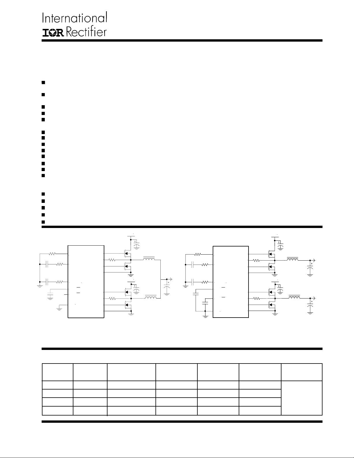
Vin
DESCRIPTION
The IR3621 IC combines a dual synchronous buck controller and drivers, providing a cost-effective, high performance
and flexible solution. The IR3621 operates in 2-Phase mode
to produce either 2-independent output voltages or current
share single output for high current application. The 180
out-of-phase operation allows the reduction of input and
output capacitance.
Other key features include two independently programmable
soft-start functions to allow system level sequencing of output voltages in various configurations. The pre-bias protection feature prevents the discharge of the output voltage and
possible damage to the load during start-up when a preexisting voltage is present at the output. Programmable
switching frequency up to 500KHz per phase allows flexibility to tune the operation of the IC to meet system level requirements, and synchronization allows the simplification
of system level filter design. Protection features such as
selectable hiccup or latched current limit, and under voltage
lock-out are provided to give required system level security
in the event of a fault condition.
Vin
IR3621
HDrv1
OCSet1
LDrv1
PGnd1
HDrv2
OCSet2
LDrv2
PGnd2
IR3621
HDrv1
OCSet1
LDrv1
PGnd1
HDrv2
OCSet2
LDrv2
PGnd2
Vout1
Vin
Vout2
Rt
Comp1
Vin
Vout
Comp2
SS1 / SD
SS2 / SD
Gnd
Rt
Comp1
Comp2
SS1 / SD
SS2 / SD
Gnd
Current share, single output configuration 2-independent output voltage configuration
Figure 1 - Typical application of IR3621 in current share single output and 2-independent output voltage configuration
ORDERING INFORMATION
PKG
DESIG
M
M
F
F
PAR T LEADFREE
NUMBER P ART NUMBER
IR3621M IR3621MPbF
IR3621MTR IR3621MTRPbF
IR3621F IR3621FPbF
IR3621FTR IR3621FTRPbF
PIN
COUNT
32
32
28
28
P ARTS
PER TUBE
73
-----50
------
P ARTS
PER REEL
------
6000
------
2500
T & R
Orientation
Fig A
www.irf.com
1
Page 2
IR3621 & ( PbF)
ABSOLUTE MAXIMUM RATINGS
Vcc, VCL Supply Voltage ........................................... -0.5V To 16V
VcH1 and VcH2 Supply Voltage ................................ -0.5V To 25V
PGOOD.................................................................... -0.5V To 16V
Storage Temperature Range ...................................... -55°C To 150°C
Junction Temperature Range ..................................... -40°C To 150°C
ESD Classification ................................................... JEDEC, JESD22-A114
Caution: Stresses above those listed in “Absolute Maximum Rating” may cause permanent damage to the device. These are stress
ratings only and function of the device at these or any other conditions beyond those indicated in the operational sections of the specifications is not implied. Exposure to “Absolute Maximum Rating” conditions for extended periods may affect device reliability
RECOMMENDED OPERATING CONDITIONS
Parameter Definition Min Max Units
Vcc Supply Voltage 5.5 14.5 V
VcH1,2 Supply Voltage 10 20 V
Fs Operating Frequency 200 500 kHz
Tj Junction Temperature -40 125 °C
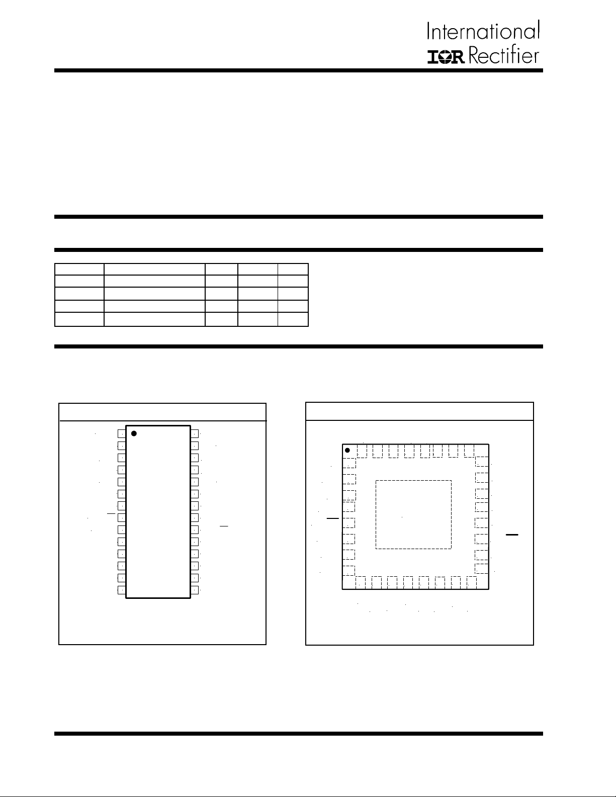
PACKAGE INFORMATION
IR3621F
28-PIN TSSOP (F)
1
PGood
2
CC
V
3
OUT3
V
4
Rt
5
SEN2
V
6
Fb2
7
Comp2
SS2 / SD
8 21
9 20
OCSet2
10 19
VcH2
11 18
HDrv2
12 17
PGnd2 HDrv1
13
LDrv2
14
CL
V
θJA = 75.5 °C/W
θJC =13.3 °C/W
28
Gnd
27
V
26
V
25
Hiccup
24
Sync
23
V
22
Fb1
Comp1
SS1 / SD
OCSet1
VcH1
16
PGnd1
15
LDrv1
REF
P2
SEN1
Rt
V
SEN2
Fb2
Comp2
SS2/SD2
OCSet2
VCH2
HDrv2
IR3621M & IR3621MPbF
32-Lead MLPQ 5mmx5mm (M)
OUT3
NC
V
Vcc
30
11
LDrv2
29
Pad
12
CL
V
3132
1
2
3
4
5
6
7
8
9
10
NC
PGnd2
PGood
13
LDrv1
REFVP2
Gnd
V
28
27
14
PGnd1
NC
26
25
15
16
NC
HDrv1
θJA = 36.0 °C/W
θJC = 1.0 °C/W
24
23
22
21
20
19
18
17
Hiccup
Sync
V
SEN1
Fb1
Comp1
SS1/SD1
OCSet1
VcH1
2
Exposed pad on underside is connected to a copper
pad through vias for 4-layer PCB board design.
www.irf.com
Page 3
IR3621 & ( PbF)
ELECTRICAL SPECIFICATIONS
Unless otherwise specified, these specifications apply over Vcc=12V , VcH1=VcH2=VCL=12V and 0°C<Tj<125°C.
PARAMETER SYMBOL TEST CONDITION MIN TYP MAX UNITS
Output V oltage Accuracy
2
0.80
1
0.75
10
15
15
10
6
6
28
0.9VREF
0.1
-0.1
100
0
1.25
300
+1
+1.35
+1.35
+1.35
+1.65
+1.65
5.3
4.0
15
25
25
15
10
10
35
0.25
0.95VREF
0.5
-0.5
2500
2500
140
+4
Vcc-2
345
0
1200
0.6
V
%
%
%
%
%
%
V
V
V
V
mA
mA
mA
mA
mA
mA
µA
V
V
V
µA
µmho
µmho
µA
mV
V
kHz
V
%
ns
%
kHz
ns
V
V
Feedback Voltage
Accuracy
UVLO Section
UVLO Threshold - Vcc
UVLO Hysteresis - Vcc
UVLO Threshold - VcH1,2
UVLO Hysteresis - VcH1,2
Supply Current Section
Vcc Dynamic Supply Current
VcH1 & VcH2 Dynamic Current
VCL Dynamic Supply Current
Vcc Static Supply Current
VcH1/VcH2 Static Current
VCL Static Supply Current
Soft-Start / SD Section
Charge Current
Shutdown Threshold
Power Good Section
VSENS1,2 Lower Trip Point
PGood Output Low Voltage
Error Amp Section
Fb Voltage Input Bias Current
Transconductance 1
Transconductance 2
Error Amp Source/Sink Current
Input Offset V oltage for E/A1,2
VP2 Voltage Range
Oscillator Section
Frequency
Ramp Amplitude
Min Duty Cycle
Min Pulse Width
Max Duty Cycle
Synch Frequency Range
Synch Pulse Duration
Synch High Level Threshold
Synch Low Level Threshold
Note1: Cold temperature performance is guaranteed via correlation using statistical quality control. Not 100% tested in production.
VFb1 , VFb2
UVLOVCC
UVLOVCH1,2
Dyn ICC
Dyn ICH
Dyn ICL
ICCQ
ICHQ
ICLQ
SSIB
SD
PGFB1,2L
PG(Voltage)
IFB1,2
gm1
gm2
I(E/A)1,2
VOS(ERR)
VP2
Freq
VRAMP
Dmin
Puls(ctrl)
Dmax
Sync(Fs)
Sync(puls)
Sync(H)
Sync(L)
Tj=25°C
MLPQ
TSSOP
Supply Ramping Up
Supply Ramp Up and Down
Supply Ramping Up
Supply Ramp Up and Down
Freq=300kHz, CL=1500pF
Freq=300kHz, CL=1500pF
Freq=300kHz, CL=1500pF
SS=0V
SS=0V
SS=0V
SS=0V
VSENS1,2 Ramping Down
ISINK=2mA
SS=3V
Fb1,2 to VREF
Note2
Rt(SET) to 30.9K
Note2
Fb=1V
FSW=300kHz, Note2
Fb=0.6V , FSW=200kHz
20% above free running freq
0°C <T
-40°C <T
Tj=25°C
0°C <Tj< 125°C
-40°C <Tj< 125°C
j< 125°C
j< 125°C
-1
-1.35
-2.5
-1.35
-1.65
-3.0
4.7
3.5
22
0.8VREF
1400
1400
60
-4
0.4
255
150
86.5
200
www.irf.com
3
Page 4
IR3621 & ( PbF)
PARAMETER SYMBOL TEST CONDITION MIN TYP MAX UNITS
OUT3 Internal Regulator
V
Output Voltage
Output Current
Protection Section
OVP Trip Threshold
OVP Fault Prop Delay
OCSET Current
Hiccup Duty Cycle
Hiccup High Level Threshold
Hiccup Low Level Threshold
Thermal Shutdown Trip Point
Thermal Shutdown Hysteresis
Output Drivers Section
LO Drive Rise Time
HI Drive Rise Time
LO Drive Fall Time
Hi Drive Fall Time
Dead Band Time
OVP
OVP(delay)
IOCSet
Tr(LO)
Tr(HI)
Tf(LO)
Tf(HI)
TDB
Output forced to 1.25VREF
Note2
Hiccup pin pulled high, Note2
Note2
Note2
Note2
Note2
CL=1500pF ,Figure 2
CL=1500pF , Figure 2
CL=1500pF ,Figure 2
CL=1500pF ,Figure 2
See Figure 2
5.8
44
1.1VREF
16
2
6.25
1.15
140
20
20
18
18
25
25
50
5
VREF
1.2
6.7
VREF
5
24
0.8
50
50
50
50
100
V
mA
V
µs
µA
%
V
V
C
C
ns
ns
ns
ns
ns
Note 2: Guaranteed by design but not tested for production.
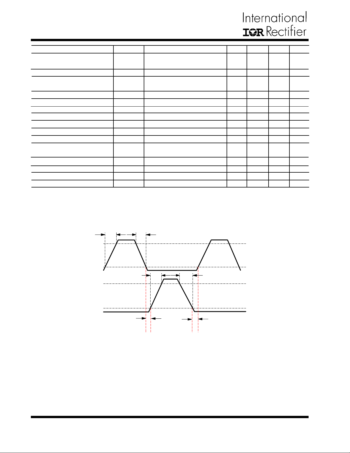
Tr
9V
High Side Driver
(HDrv )
2V
9V
Low Side Driver
(LDrv)
2V
Deadband
H_to_L
Tf
Tr
Tf
Deadband
L_to_H
4
Figure 2 - Rise Time, Fall Time and Deadband for Driver Section
www.irf.com
Page 5
PIN DESCRIPTIONS
TSSOP MLPQ PIN SYMBOL PIN DESCRIPTION
1
2
3
4
5,23
6,22
7,21
8
20
9,19
10,18
1 1,17
12,16
13,15
14
24
25
26
27
28
29
30
31
1
2,22
3,21
4,20
5
19
6,18
7,17
8,16
10,14
1 1,13
12
23
24
26
27
28
9,15,25.32
PGood
Vcc
VOUT3
Rt
VSEN2, VSEN1
Fb2,Fb1
Comp2, Comp1
SS2 / SD
SS1 / SD
OCSet2,OCSet1
VcH2, VcH1
HDrv2, HDrv1
PGnd2, PGnd1
LDrv2, LDrv1
V
CL
Sync
Hiccup
VP2
VREF
Gnd
N/C
Power Good pin. Low when any of the outputs fall 10% below the set voltages.
Supply voltage for the internal blocks of the IC. The Vcc slew rate should be
<0.1V/us.
Output of the internal LDO. Connect a 1.0uF capacitor from this pin to ground.
Connecting a resistor from this pin to ground sets the oscillator frequency .
Sense pins for OVP and PGood. For current share tie these pins together.
Inverting inputs to the error amplifiers. In current sharing mode, Fb1 is connected to a resistor divider to set the output voltage and Fb2 is connected to
programming resistor to achieve current sharing. In independent 2-channel mode,
these pins work as feedback inputs for each channel.
Compensation pins for the error amplifiers.
These pins provide user programmable soft-start function for each outputs.
Connect external capacitors from these pins to ground to set the start up time
for each output. These outputs can be shutdown independently by pulling the
respective pins below 0.3V . During shutdown both MOSFET s will be turned of f.
For current share mode SS2 must be floating.
A resistor from these pins to switching point will set current limit threshold.
Supply voltage for the high side output drivers. These are connected to voltages
that must be typically 6V higher than their bus voltages. A 0.1µF high frequency capacitor must be connected from these pins to PGND to provide peak
drive current capability .
Output drivers for the high side power MOSFET s. Note3
These pins serve as the separate grounds for MOSFET drivers and should be
connected to the system’s ground plane.
Output drivers for the synchronous power MOSFET s.
Supply voltage for the low side output drivers.
The internal oscillator can be synchronized to an external clock via this pin.
When pulled High, it puts the device current limit into a hiccup mode. When
pulled Low, the output latches of f, after an overcurrent event.
Non-inverting input to the second error amplifier. In the current sharing mode, it
is connected to the programming resistor to achieve current sharing. In independent 2-channel mode it is connected to V
the resistor divider to set the output voltage.
Reference Voltage. The drive capability of this pin is about 2µA.
Analog ground for internal reference and control circuitry .
No Connect
IR3621 & ( PbF)
REF pin when Fb2 is connected to
Note3: The negative voltage at these pins may cause instability for the gate drive circuits. To prevent this, a low
forward voltage drop diode (Schottky) is required between these pins and power ground.
www.irf.com
5
Page 6
IR3621 & ( PbF)
BLOCK DIAGRAM
Vcc
28uA
28uA
SS2 / SD
SS1 / SD
POR
Fb1
Comp1
Rt
Sync
V
REF
V
P2
Fb2
Comp2
V
SEN1
V
SEN2
0.8V
64uA
0.8V
64uA
Max
Error Amp1
Error Amp2
Mode
VcH1
VcH2
Ramp1
Ramp2
2
SS
0.8V
PWM Comp1
Two Phase
Osc illator
PWM Comp2
PGood / O V P
Mode
Control
Bias
Generator
UVLO
Set1
Set2
0.3V
SS2
POR
Mode
3V
0.8V
POR
Thermal
Shutdown
R
Q
S
Reset Dom
Reset Dom
S
Q
R
POR
OVP
HDrv OFF / LDrv ON
SS1
SS2
Mode
0.3V
SS1
Hiccup
Control
SS1
S
R
Q
SS2
3uA
3uA
POR
PBias1
PBias2
20uA
20uA
S
Q
PBias1
R
VcH1
HDrv1
V
CL
LDrv1
PGnd1
OCSet1
VcH2
HDrv2
Hiccup
LDrv2
PGnd2
OCSet2
6
Gnd
Regulator
Figure 3 - IR3621Block Diagram
www.irf.com
PGood
V
OUT3
Page 7
FUNCTIONAL DESCRIPTION
Introduction
The IR3621 is a versatile device for high performance
buck converters. It consists of two synchronous buck
controllers which can be operated either in two independent mode or in current share mode.
The timing of the IC is provided by an internal oscillator
circuit which generates two out-of-phase clock that can
be programmed up to 500kHz per phase.
Supply Voltage
Vcc is the supply voltage for internal controller. The operating range is from 5.5V to 14.5V . It also is fed to the
internal LDO. When Vcc is below under-voltage threshold, all MOSFET drivers will be turned off.
Internal Regulator
The regulator powers directly from Vcc and generates a
regulated voltage (Typ. 6.2V@40mA). The output is protected for short circuit. This voltage can be used for charge
pump circuitry as shown in Figure12.
IR3621 & ( PbF)
In this mode, one control loop acts as a master and sets
the output voltage as a regular Voltage Mode Buck controller and the other control loop acts as a slave and
monitors the current information for current sharing. The
voltage drops across the current sense resistors (or DCR
of inductors) are measured and their difference is amplified by the slave error amplifier and compared with the
ramp signal to generate the PWM pulses to match the
output current. In this mode the SS2 pin should be floating.
IR3621
PWM Comp1
PWM Comp2
Master E/A
Comp
0.8V
Fb1
VP2
V
L1
R1
C1
OUT
R
L1
Input Supplies UnderV oltage LockOut
The IR3621 UVLO block monitors three input voltages
(Vcc, VcH1 and VcH2) to ensure reliable start up. The
MOSFET driver output turn off when any of the supply
voltages drops below set thresholds. Normal operation
resumes once the supply voltages rise above the set
values.
Mode Selection
The SS2 pin is used for mode selection. In current share
mode this pin should be floating and in dual output mode
a soft start capacitor must be connected from this pin to
ground to program the start time for the second output.
Independent Mode
In this mode the IR3621 provides control to two independent output power supplies with either common or different input voltages. The output voltage of each individual
channel is set and controlled by the output of the error
amplifier, which is the amplified error signal from the
sensed output voltage and the reference voltage. The
error amplifier output voltage is compared to the ramp
signal thus generating fixed frequency pulses of variable
duty-cycle, which are applied to the FET drivers, Figure19 shows a typical schematic for such application.
FB2
Slave E/A
L2
L2
R
R2
C2
Figure 4 - Loss-less inductive current sensing
and current sharing.
In the diagram, L1 and L2 are the output inductors. RL1
and RL2 are inherent inductor resistances. The resistor
R1 and capacitor C1 are used to sense the average inductor current. The voltage across the capacitors C1
and C2 represent the average current flowing into resistance RL1 and RL2. The time constant of the RC network
should be equal or at most three times larger than the
time constant L1/RL1.
R1×C1=(1~3)× ---(1)
L1
RL1
Currnt Share Mode
This feature allows to connect both outputs together to
increase current handling capability of the converter to
support a common load. The current sharing can be done
either using external resistors or sensing the DCR of
inductors (see Figure 4).
www.irf.com
Figure 5 - 30A Current Sharing using Inductor sensing
(5A/Div)
7
Page 8
IR3621 & ( PbF)
Dual Soft-Start
The IR3621 has programmable soft-start to control the
output voltage rise and limit the inrush current during
start-up. It provides a separate Soft-Start function for each
outputs. This will enable to sequence the outputs by
controlling the rise time of each output through selection
of different value soft-start capacitors. The soft-start pins
will be connected together for applications where, both
outputs are required to ramp-up at the same time.
To ensure correct start-up, the soft-start sequence initiates when the Vcc, VcH1 and VcH2 rise above their
threshold and generate the Power On Reset (POR) signal. Soft-start function operates by sourcing an internal
current to charge an external capacitor to about 3V . Initially, the soft-start function clamps the E/A’s output of
the PWM converter. During power up, the converter output starts at zero and thus the voltage at Fb is about 0V .
A current (64µA) injects into the Fb pin and generates a
voltage about 1.6V (64µA×25K) across the negative
input of E/A and (see Figure6).
The magnitude of this current is inversely proportional to
the voltage at soft-start pin. The 28µA current source
starts to charge up the external capacitor. In the mean
time, the soft-start voltage ramps up, the current flowing
into Fb pin starts to decrease linearly and so does the
voltage at negative input of E/A.
SS2 / SD
SS1 / SD
POR
Fb1
Comp1
V
P2
Fb2
Comp2
28uA
28uA
64uA
8
20
0.8V
22
21
26
6
7
Max
64uA
Error Amp1
Error Amp2
Figure 6 -Soft-start circuit for IR3621
Output of POR
3V
When the soft-start capacitor is around 1V , the current
flowing into the Fb pin is approximately 32µA. The voltage at the positive input of the E/A is approximately:
32µA×25K = 0.8V
The E/A will start to operate and the output voltage starts
to increase. As the soft-start capacitor voltage continues to go up, the current flowing into the Fb pin will keep
decreasing. Because the voltage at pin of E/A is regulated to reference voltage 0.8V , the voltage at the Fb is:
VFB = 0.8-(25K×Injected Current)
The feedback voltage increases linearly as the injecting
current goes down. The injecting current drops to zero
when soft-start voltage is around 1.8V and the output
voltage goes into steady state. Figure 7 shows the theoretical operational waveforms during soft-start.
Low Temperature Start-Up
The controller is capable of starting at -40C ambient
temperature.
≅
1.8V
≅
Soft-Start
Voltage
Current flowing
into Fb pin
Voltage at negative input
of Error Am p
Voltage at Fb pin
0V
64uA
≅
1.6V
0V
1V
0uA
0.8V
0.8V
Figure 7 - Theoretical operational waveforms
during soft-start.
The output start-up time is the time period when softstart capacitor voltage increases from 1V to 1.8V. The
start-up time will be dependent on the size of the external soft-start capacitor. The start-up time can be estimated by:
28µA×TSTART/CSS = 1.8V-1V
8
www.irf.com
Page 9
IR3621 & ( PbF)
For a given start up time, the soft-start capacitor can be
calculated by:
SS ≅ 28µA×TSTART/0.8V
C
The soft-start is part of the Over Current Protection
scheme, during the overload or short circuit condition
the external soft start capacitors will be charged and
discharged in certain slope rate to achieve the hiccup
mode function.
SS1 / SD
28uA
Hiccup
20
3uA
Figure 8 - 3uA current source for discharging soft
start-capacitor during Hiccup mode
Out-of-Phase Operation
The IR3621 drives its two output stages 180 out-of-phase.
In 2-phase configuration, the two inductor ripple currents
cancel each other and result in a reduction of the output
current ripple and yield a smaller output capacitor for the
same ripple voltage requirement.
In single input voltage applications, the input ripple current
reduces. This results in much smaller input capacitor's
RMS current and reduces the input capacitor quantity .
Over-Current Protection
The IR3621 can provide two different schemes for OverCurrent Protection (OCP). When the Hiccup pin is pulled
high, the OCP will operate in hiccup mode. In this mode,
during overload or short circuit, the outputs enter hiccup
mode and stay in that mode until the overload or short
circuit is removed. The converter will automatically recover.
When the Hiccup pin is pulled low, the OCP scheme
will be changed to the latch up type, in this mode the
converter will be turned off during Overcurrent or short
circuit. The power needs to be recycled for normal
operation.
Each phase has its own independent OCP circuitry.
The OCP is performed by sensing current through the
R
DS(ON) of low side MOSFET. As shown in Figure 9, an
external resistor (RSET) is connected between OCSet pin
and the drain of low side MOSFET (Q2) which sets the
current limit set point.
If using one soft start capacitor in dual configuration for a
precise power up the OCP needs to be set to latch mode.
The internal current source develops a voltage across
RSET. When the low side switch is turned on, the inductor current flows through the Q2 and results a voltage
which is given by:
OCSET = IOCSET×RSET-RDS(ON)×iL ---(2)
V
I
OCSET
Hiccup
Control
IR3621
OCSet
R
SET
Q1
Q2
V
L1
OUT
Figure 9 - Diagram of the over current sensing.
The critical inductor current can be calculated by setting:
V
OCSET = IOCSET×RSET - RDS(ON)×IL = 0
RSET×IOCSET
ISET = IL(CRITICAL)= ---(3)
RDS(ON)
The value of RSET should be checked in an actual
circuit to ensure that the Over Current Protection
circuit activates as expected. The IR3621 current limit
is designed primarily as disaster preventing, "no blow
up" circuit, and is not useful as a precision current
regulator.
In two independent mode, the output of each channel
is protected independently which means if one output
is under overload or short circuit condition, the other
output will remain functional. The OCP set limit can be
programmed to different levels by using the external
resistors. This is valid for both hiccup mode and latch
up mode.
In 2-phase configuration, the OCP's output depends on
any one channel, which means as soon as one
channel goes to overload or short circuit condition the
output will enter either hiccup or latch-up, dependes on
status of Hiccup pin.
Pre-bias Startup
The IR3621 allows pre-bias startup without discharging
the output capacitors. The output starts in asynchronous fashion and keeps the synchronous MOSFET off
until the first gate signal for control MOSFET is generated.
www.irf.com
9
Page 10

IR3621 & ( PbF)
Frequency Synchronization
The IR3621 is capable of accepting an external digital
synchronization signal. Synchronization will be enabled
by the rising edge at an external clock. Per-channel switching frequency is set by external resistor (Rt). The free
running oscillator frequency is twice the per-channel frequency . During synchronization, Rt is selected such that
the free running frequency is 20% below the sync frequency . Synchronization capability is provided for both 2output and 2-phase configurations. When unused, the
Sync pin will remain floating and is noise immune.
Thermal Shutdown
T emperature sensing is provided inside IR3621. The trip
threshold is typically set to 140C. When trip threshold is
exceeded, thermal shutdown turns off both MOSFETs.
Thermal shutdown is not latched and automatic restart is
initiated when the sensed temperature drops to normal
range. There is a 20C hysteresis in the shutdown threshold.
Power Good
The IR3621 provides a power good signal. The power good
signal should be available after both outputs have reached
regulation. This pin needs to be externally pulled high.
High state indicates that outputs are in regulation.
Power good will be low if either one of the output voltages
is 10% below the set value. There is only one power good
for both outputs.
Operation Frequency Selection
The optimum operating frequency range for the IR3621
is 300kHz per phase, theoretically the IR3621 can be
operated at higher switching frequency (e.g. 500kHz).
However the power dissipation for IC, which is function
of applied voltage, gate drivers load and switching frequency , will result in higher junction temperature of device. It may exceed absolute maximum rating of junction temperature, figure 18 (page 17) shows case temperature versus switching frequency with different capacitive loads for TSSOP package.
This should be considered when using IR3621 for such
application. The below equation shows the relationship
between the IC's maximum power dissipation and Junction temperature:
Where:
Pd =
ΤJ-ΤA
θJA
Tj: Maximum Operating Junction T emperature
T A: Ambient T emperature
θ
JA = Thermal Impedance of package
The switching frequency is determined by an external
resistor (Rt). The switching frequency is approximately
inversely proportioned to resistance (see Fig 10).
Per Ch a n n el Switching F requ en c y vs. RT
700
Over-V oltage Protection OVP
Over-voltage is sensed through separate V
OUT sense pins
VSEN1 and VSEN2. A separate OVP circuit is provided for
each output. Upon over-voltage condition of either one of
the outputs, the OVP forces a latched shutdown on both
outputs. In this mode, the upper FET drivers turn off and
the lower FET drivers turn on, thus crowbaring the outputs. Reset is performed by recycling Vcc.
Error Amplifier
The IR3621 is a voltage mode controller. The error amplifiers are of transconductance type. In independent mode,
each amplifier closes the loop around its own output voltage. In current sharing mode, amplifier 1 becomes the
master which regulates the common output voltage. Amplifier 2 performs the current sharing function. Both amplifiers are capable of operating with Type III compensation control scheme.
600
500
400
300
200
Switching Frequency (kHz)
100
0
0 10203040506070
RT (kohm)
Figure 10- Switching Frequency versus External Resistor.
Shutdown
The outputs can be shutdown independently by pulling
the respective soft-start pins below 0.3V. This can be
easily done by using an external small signal transistor. During shutdown both MOSFETs will be turned off.
During this mode the LDO will stay on. Normal operation will resume by cycling soft start pins.
10
www.irf.com
Page 11

IR3621 & ( PbF)
APPLICATION INFORMATION
Design Example:
The following example is a typical application for the
IR3621, the schematic is Figure19 on page18.
IN = 12V
V
VOUT(2.5V) = 2.5V @ 10A
VOUT(1.8V) = 1.8V @ 10A
∆VOUT = Output voltage ripple ≅ 3% of VOUT
FS = 400kHz
Output Voltage Programming
Output voltage is programmed by the reference voltage
and an external voltage divider. The Fb1 pin is the inverting input of the error amplifier, which is referenced to the
voltage on the non-inverting pin of error amplifier. For this
application, this pin (V
voltage (VREF). The output voltage is defined by using the
following equation:
VOUT = VP2 × 1 +
VP2 = VREF = 0.8V
When an external resistor divider is connected to the
output as shown in Figure 1 1.
V
V
Figure 1 1 - Typical application of the IR3621 for pro-
gramming the output voltage.
Equation (4) can be rewritten as:
R6 = R5 ×
Will result to:
VOUT(2.5V) = 2.5V
VREF = 0.8V
R9= 2.15K, R5= 1K
If the high value feedback resistors are used, the input
bias current of the Fb pin could cause a slight increase
in output voltage. The output voltage can be set more
accurately by using low value, precision resistors.
P2) is connected to the reference
R6
---(4)
R5
( )
IR3621
REF
P2
Fb
VOUT
- 1
( )
VP
VOUT(1.8V) = 1.8V
VREF = 0.8
R7= 1.24K, R8 = 1K
V
OUT
6
R
5
R
Soft-Start Programming
The soft-start timing can be programmed by selecting
the soft-start capacitance value. The start-up time of
the converter can be calculated by using:
Css ≅ 28×tSTART (µF) ---(5)
Where tSTART is the desired start-up time (ms)
For a start-up time of 4ms for both output, the soft-start
capacitor will be 0.1µF. Connect two 0.1µFceramic
capacitors from SS1 pin and SS2 pin to GND.
Supply VcH1 and VcH2
T o drive the high side MOSFET, it is necessary to supply a gate voltage at least 4V greater than the bus voltage. This is achieved by using a charge pump configuration as shown in Figure 12. This method is simple
and inexpensive. The operation of the circuit is as follows: when the lower MOSFET is turned on, the capacitor (C1) charges up to VOUT3, through the diode
(D1). The bus voltage will be added to this voltage when
upper MOSFET turns on in next cycle, and providing
supply voltage (VcH1) through diode (D2). VcH1 is approximately:
VCH1 ≅ VOUT3 + VBUS - (VD1 + VD2)
Capacitor in the range of 0.1µF is generally adequate
for most applications. The diode must be a fast recovery device to minimize the amount of charge fed back
from the charge pump capacitor into VOUT3. The diodes
need to be able to block the full power rail voltage, which
is seen when the high side MOSFET is switched on.
For low voltage application, Schottky diodes can be
used to minimize forward drop across the diodes at
start up.
D1
Regulator
IR3621
V
OUT3
Figure 12 - Charge pump circuit.
VcH1
C3
HDrv
C2
D2
C1
BUS
V
Q1
L2
Q2
www.irf.com
11
Page 12

IR3621 & ( PbF)
Input Capacitor Selection
The 1800 out of phase will reduce the RMS value of the
ripple current seen by input capacitors. This reduces
numbers of input capacitors. The input capacitors must
be selected that can handle both the maximum ripple
RMS at highest ambient temperature as well as the
maximum input voltage. The RMS value of current ripple
for duty cycles under 50% is expressed by:
= (I
2
D1(1-D1)+I
1
I
RMS
2
D2(1-D2)-2I1I2D1D2) --- (6)
2
Where:
is the RMS value of the input capacitor current
I
RMS
D1 and D2 are the duty cycle for each output
I1 and I2 are the current for each output
For this application the I
RMS
=4.8A
For higher efficiency, low ESR capacitors are recommended.
Choose two Poscap from Sanyo 16TPB47M (16V , 47µF,
70mΩ ) with a maximum allowable ripple current of 1.4A
for inputs of each channel.
Inductor Selection
The inductor is selected based on operating frequency ,
transient performance and allowable output voltage ripple.
Low inductor values result in faster response to step
load (high ∆i/∆t) and smaller size but will cause larger
output ripple due to increased inductor ripple current. As
a rule of thumb, select an inductor that produces a ripple
current of 10-40% of full load DC.
For the buck converter, the inductor value for desired
operating ripple current can be determined using the following relation:
VIN - VOUT = L× ; ∆t = D× ; D =
L = (VIN - VOUT)× ---(7)
∆i
∆t
VOUT
VIN×∆i×fS
1
fS
VOUT
VIN
Where:
VIN = Maximum Input V oltage
VOUT = Output Voltage
∆i = Inductor Ripple Current
fS = Switching Frequency
∆t = Turn On Time
D = Duty Cycle
For ∆i(2.5V) = 45%(IO(2.5V) ), then the output inductor will
be:
L4 = 1.1µH
For ∆i(1.8V) = 35%(IO(1.8V) ), then the output inductor will
be:
L3 = 1.1µH
Panasonic provides a range of inductors in different values and low profile for large currents.
Choose ETQP6F1R1BFA (1.1µH, 16A, 2.2mΩ) both for
L3 and L4.
For 2-phase application, equation (7) can be used for
calculating the inductors value. In such case the inductor ripple current is usually chosen to be between 1040% of maximum phase current.
Output Capacitor Selection
The criteria to select the output capacitor is normally
based on the value of the Effective Series Resistance
(ESR). In general, the output capacitor must have low
enough ESR to meet output ripple and load transient
requirements, yet have high enough ESR to satisfy stability requirements. The ESR of the output capacitor is
calculated by the following relationship:
(ESL, Equivalent Series Inductance is neglected)
ESR ≤ ---(8)
∆VO
∆IO
Where:
∆VO = Output Voltage Ripple
∆i = Inductor Ripple Current
∆VO = 3% of VO will result to ESR(2.5V) =16.6mΩ and
ESR(1.8V) =16mΩ
The Sanyo TPC series, Poscap capacitor is a good choice.
The 6TPC330M, 330µF, 6.3V has an ESR 40mΩ. Se-
lecting three of these capacitors in parallel for 2.5V output, results to an ESR of ≅ 13.3mΩ which achieves our
low ESR goal. And selecting three of these capacitors in
parallel for 1.8V output, results in an ESR of ≅ 13.3mΩ
which achieves our low ESR goal.
The capacitors value must be high enough to absorb the
inductor's ripple current.
Power MOSFET Selection
The IR3621 uses four N-Channel MOSFET s. The selection criteria to meet power transfer requirements is based
on maximum drain-source voltage (VDSS), gate-source
drive voltage (VGS), maximum output current, On-resistance RDS(ON) and thermal management.
The both control and synchronous MOSFET s must have
a maximum operating voltage (VDSS) that exceeds the
maximum input voltage (VIN).
12
www.irf.com
Page 13

IR3621 & ( PbF)
The gate drive requirement is almost the same for both
MOSFET s. Logic-level transistors can be used and caution should be taken with devices at very low V
GS to pre-
vent undesired turn-on of the complementary MOSFET ,
which results in a shoot-through.
The total power dissipation for MOSFET s includes conduction and switching losses. For the Buck converter,
the average inductor current is equal to the DC
load current. The conduction loss is defined as:
PCOND(Upper Switch) = ILOAD×RDS(on)×D×ϑ
PCOND(Lower Switch) = ILOAD×RDS(on)×(1 - D)×ϑ
2
2
ϑ = RDS(on) T emperature Dependency
The R
DS(ON) temperature dependency should be consid-
ered for the worst case operation. This is typically given
in the MOSFET data sheet. Ensure that the conduction
losses and switching losses do not exceed the package
ratings or violate the overall thermal budget.
Choose IRF7821 for control MOSFET s and IRF81 13 for
synchronous MOSFET s. These devices provide low onresistance in a compact SOIC 8-Pin package.
VDS(OFF)
P
SW = ILOAD ---(9)
2
×
tr + tf
T
×
Where:
VDS(OFF) = Drain to Source Voltage at of f time
tr = Rise Time
tf = Fall Time
T = Switching Period
LOAD = Load Current
I
V
DS
90%
10%
V
GS
t
d
t
d
(ON)
(OFF )
t
r
t
Figure 13 - Switching time waveforms.
From IRF7821 data sheet we obtain:
IRF7821
tr = 2.7ns
tf = 7.3ns
f
The MOSFET s have the following data:
IRF7821
VDSS = 30V
RDS(on) = 9mΩ
IRF81 13
VDSS = 30V
RDS(on) = 6mΩ
The total conduction losses for each output will be:
PCON(TOTAL, 2.5V) = PCON(UPPER) + PCON(LOWER)
PCON(TOTAL, 2.5V) = 1.0W
PCON(TOTAL, 1.8V) = PCON(UPPER) + PCON(LOWER)
PCON(TOTAL, 1.8V) = 1.0W
The switching loss is more difficult to calculate, even
though the switching transition is well understood. The
reason is the effect of the parasitic components and
switching times during the switching procedures such
as turn-on / turnoff delays and rise and fall times. The
control MOSFET contributes to the majority of the switching losses in a synchronous Buck converter. The synchronous MOSFET turns on under zero voltage conditions, therefore, the switching losses for synchronous
MOSFET can be neglected. With a linear approximation, the total switching loss can be expressed as:
These values are taken under a certain condition test.
For more details please refer to the IRF7821 data sheet.
By using equation (9), we can calculate the total switching losses.
PSW(TOTAL,2.5V) = 0.18W
PSW(TOTAL,1.8V) = 0.18W
Programming the Over-Current Limit
The over-current threshold can be set by connecting a
resistor (RSET) from drain of low side MOSFET to the
OCSet pin. The resistor can be calculated by using equation (3).
The RDS(on) has a positive temperature coefficient and it
should be considered for the worse case operation.
RDS(on) = 6mΩ×1.5 = 9mΩ
ISET ≅ IO(LIM) = 10A×1.5 = 15A
(50% over nominal output current)
This results to:
RSET = R1=R6=6.75KΩ
This resistor must be placed close to the IC, place a
small ceramic capacitor from this pin to ground for noise
rejection purposes.
www.irf.com
13
Page 14

IR3621 & ( PbF)
Feedback Compensation
The IR3621 is a voltage mode controller; the control loop
is a single voltage feedback path including error amplifier and error comparator. To achieve fast transient response and accurate output regulation, a compensation
circuit is necessary . The goal of the compensation network is to provide a closed loop transfer function with
the highest 0dB crossing frequency and adequate phase
margin (greater than 45).
The output LC filter introduces a double pole, –40dB/
decade gain slope above its corner resonant frequency ,
and a total phase lag of 180 (see Figure 14). The Resonant frequency of the LC filter is expressed as follows:
FLC = ---(10)
Where: Lo is the output inductor
For 2-phase application, the effective output
inductance should be used
Co is the total output capacitor
Figure 14 shows gain and phase of the LC filter. Since
we already have 180 phase shift just from the output
filter, the system risks being unstable.
1
2π× LO×CO
The ESR zero of the output capacitor is expressed as
follows:
FESR = ---(10A)
V
1
2π×ESR×Co
OUT
9
R
Fb
Comp
R
5
Vp=V
E/A
REF
Gain(dB)
Ve
C
9
C
R
4
POLE
H(s) dB
Frequency
F
Z
Figure 15 - Compensation network without local
feedback and its asymptotic gain plot.
The transfer function (Ve / V
OUT) is given by:
0dB
Gain
-40dB/decade
LC
F
Frequency
-180
Phase
0
LC
F
Frequency
Figure14 - Gain and phase of LC filter
The IR3621’s error amplifier is a differential-input transconductance amplifier. The output is available for DC gain
control or AC phase compensation.
The E/A can be compensated with or without the use of
local feedback. When operated without local feedback,
the transconductance properties of the E/A become evident and can be used to cancel one of the output filter
poles. This will be accomplished with a series RC circuit
from Comp pin to ground as shown in Figure 15.
Note that this method requires the output capacitor to
have enough ESR to satisfy stability requirements. In
general, the output capacitor’s ESR generates a zero
typically at 5kHz to 50kHz which is essential for an acceptable phase margin.
H(s) = gm× × ---(11)
( )
R5
R9 + R5
1 + sR4C9
sC9
The (s) indicates that the transfer function varies as a
function of frequency . This configuration introduces a gain
and zero, expressed by:
|H(s=j×2π×FO)| = gm× ×R4 ---(12)
FZ = ---(13)
1
2π×R4×C9
R5
R9+R5
|H(s)| is the gain at zero cross frequency .
First select the desired zero-crossover frequency (FO1):
FO1 > FESR and FO1 ≤ (1/5 ~ 1/10)×fS
14
www.irf.com
Page 15

IR3621 & ( PbF)
1
gm
VIN
FO1×FESR
2
FLC
R5 + R9
R5
VOSC
R4 = × × × ---(14)
Where:
VIN = Maximum Input Voltage
VOSC = Oscillator Ramp Voltage
FO1 = Crossover Frequency
FESR = Zero Frequency of the Output Capacitor
FLC = Resonant Frequency of the Output Filter
R5 and R9 = Resistor Dividers for Output Voltage
Programming
g
m = Error Amplifier Transconductance
For V2.5V:
VIN = 12V
VOSC = 1.25V
FO1 = 40KHz
FESR = 13.3kHz
FLC = 5.06kHz
R5 = 1K
R9 = 2.14K
gm = 1400µmho
This results to R4=4.8K
Choose R4=5K
To cancel one of the LC filter poles, place the zero before the LC filter resonant frequency pole:
FZ ≅ 75%FLC
FZ ≅ 0.75×
1
---(15)
2π LO × CO
For:
Lo = 1.1µH
Co = 990µF
FZ = 3.61kHz
R4 = 5K
Using equations (13) and (15) to calculate C9, we get:
C9 ≅ 8.3nF; Choose C9 =8.2nF
Same calcuation For V1.8V will result to: R3 = 4.2K and
C8 = 10nF
One more capacitor is sometimes added in parallel with
C9 and R4. This introduces one more pole which is mainly
used to suppress the switching noise. The additional
pole is given by:
FP =
2π×R4×
1
C9×CPOLE
C9 + CPOLE
The pole sets to one half of switching frequency which
results in the capacitor CPOLE:
CPOLE = ≅
π×R4×fS -
for FP <<
1
1
C9
fS
2
1
π×R4×fS
For a general solution for unconditional stability for ceramic output capacitor with very low ESR or any type of
output capacitors, in a wide range of ESR values we
should implement local feedback with a compensation
network. The typically used compensation network for a
voltage-mode controller is shown in Figure 16.
V
Z
IN
Gain(dB)
OUT
C
10
R
8
R
6
Fb
R
5
VP2=V
REF
R
7
E/A
C
12
C
11
Z
f
Comp
Ve
H(s) dB
F
Z
1
F
P
F
Z
2
2
Frequency
F
P
3
Figure 16- Compensation network with local
feedback and its asymptotic gain plot.
In such configuration, the transfer function is given by:
Ve
VOUT
1 - gmZf
=
1 + gmZIN
The error amplifier gain is independent of the transconductance under the following condition:
gmZf >> 1 and gmZIN >>1 ---(16)
By replacing ZIN and Zf according to Figure 16, the transformer function can be expressed as:
H(s) =
1
sR6(C12+C11)
(1+sR7C11)×[1+sC10(R6+R8)]
×
1+sR7
[ ( )]
C12C11
×(1+sR8C10)
C12+C11
As known, transconductance amplifier has high impedance (current source) output, therefore, consider should
be taken when loading the E/A output. It may exceed its
source/sink output current capability , so that the amplifier will not be able to swing its output voltage over the
necessary range.
The compensation network has three poles and two zeros and they are expressed as follows:
www.irf.com
15
Page 16

IR3621 & ( PbF)
FP1 = 0
FP2 =
FP3 = ≅
FZ1 =
FZ2 = ≅
Cross Over Frequency:
O = R7×C10× ×
F
Where:
VIN = Maximum Input V oltage
VOSC = Oscillator Ramp Voltage
Lo = Output Inductor
Co = T otal Output Capacitors
The stability requirement will be satisfied by placing the
poles and zeros of the compensation network according
to following design rules. The consideration has been
taken to satisfy condition (16) regarding transconductance error amplifier.
These design rules will give a crossover frequency approximately one-tenth of the switching frequency. The
higher the band width, the potentially faster the load transient response. The DC gain will be large enough to provide high DC-regulation accuracy (typically -5dB to -12dB).
The phase margin should be greater than 45 for overall
stability.
Based on the frequency of the zero generated by ESR
versus crossover frequency , the compensation type can
be different. The table below shows the compensation
type and location of crossover frequency .
Compensator
Type
Type II (PI)
Type III (PID)
Method A
Type III (PID)
Method B
T able - The compensation type and location of zero
Details are dicussed in application Note AN-1043 which
can be downloaded from the IR Web-Site.
1
2π×R8×C10
1
2π×R7×
2π×R
2π×C
Crossover Frequency
FLC < FESR < FO < fS/2
FLC < FO < FESR < fS/2
FLC < FO < fS/2 < FZO
crossover frequency .
C12×C11
( )
C12+C11
1
7×C11
1
10×(R6 + R8)
VIN
VOSC12π×Lo×Co
Location of Zero
(FO)
1
2π×R7×C12
1
2π×C10×R6
---(17)
Typical
Output
Capacitor
Electrolytic,
Tantalum
Tantalum,
Ceramic
Ceramic
Compensation for Slave Error Amplfier for 2-Phase
Configuration
The slave error amplifier is a differential-input transconductance amplifier, in 2-phase configuration the main goal
for the slave feed back loop is to control the inductor
current to match the master's inductor current as well
provides highest bandwidth and adequate phase margin
for overall stability . The following analysis is valid for both
using external current sense resistor and using DCR of
inductors.
The transfer function of power stage is expressed by:
G(s) = = ---(18)
Where:
VIN = Input Voltage
L2 = Output Inductor
VOSC = Oscillator Peak Voltage
As shown the transfer function is a function of inductor
current.
The transfer function for the compensation network is
given by equation (19), when using a series RC circuit
as shown in Figure 17:
D(s) = =
The loop gain function is:
H(s)=[G(s) × D(s) × RS2]
H(s)=RS2×
IL2(s)
Ve(s)
Ve(s)
RS2 × IL2(s)
R
S2
R
S1
Figure 17 - The PI compensation network
gm×
VIN
sL2 × VOSC
RS1
gm×
( )
RS2
I
L2
L
2
Fb2
E/A2
Vp2
L
1
I
L1
for slave channel.
RS1
RS2
×
( )( )
1+sR2C2
sC2
1 + sC2R2
×
( )
sC2
Comp2
R
2
C
2
×
( )
sL2×VOSC
---(19)
Ve
VIN
16
www.irf.com
Page 17

IR3621 & ( PbF)
)
Select a zero crossover frequency for control loop (FO2)
1.25 times larger than zero crossover frequency for voltage loop (FO1):
Fo2 ≅ 1.25%xF01
H(Fo) = gm×RS1×R2× =1 ---(20)
2π×Fo×L2×VOSC
VIN
From (20), R2 can be express as:
R2 = ×
1
gm × RS1
2π × F
O2 × L2 × VOSC
VIN
---(21)
The power stage of current loop has a dominant pole (Fp)
at frequency expressed by:
Req
F
p =
2π×L2
Where Req is the total resistance of the power stage
which includes the Rds(on) of the FET switches, the DCR
of inductor and shunt resistance (if it used).
Req=RDS(on)+RL+Rs
Set the zero of compensator at 10 times the dominant
pole frequency Fp, the compensator capacitor, C2 can
be calculated as:
Fz = 10 x Fp
C2 =
1
2πxR2xFz
All design should be tested for stability to verify the calculated values.
Layout Consideration
The layout is very important when designing high frequency switching converters. Layout will affect noise
pickup and can cause a good design to perform with
less than expected results.
Start by placing the power components. Make all the
connections in the top layer with wide, copper filled areas. The inductor, output capacitor and the MOSFET
should be as close to each other as possible. This helps
to reduce the EMI radiated by the power traces due to
the high switching. Place input capacitor near to the
drain of the high-side MOSFET .
The layout of driver section should be designed for a low
resistance (a wide, short trace) and low inductance (a
wide trace with ground return path directly beneath it),
this directly affects the driver's performance.
T o reduce the ESR, replace the one input capacitor with
two parallel ones. The feedback part of the system should
be kept away from the inductor and other noise sources
and must be placed close to the IC. In multilayer PCBs,
use one layer as power ground plane and have a separate control circuit ground (analog ground), to which all
signals are referenced. The goal is to localize the high
current paths to a separate loops that does not interfere
with the more sensitive analog control function. These
two grounds must be connected together on the PC board
layout at a single point.
Switching Frequency v s. Case Temp
90
80
70
60
50
Case temp (oC
40
30
200 300 400 500 600 700
Freq (kHz)
100pF
1000pF
1800pF
3300pF
Figure18- Case Temperature (TSSOP package) versus Switching Frequency at
Room T emperature
Test Condition: Vin=VcL=VcH1=VcH2=12V, Capacitors used as loads for output
drivers.
www.irf.com
17
Page 18

IR3621 & ( PbF)
TYPICAL APPLICATION
D1
C12
12V
C1
PGood
C10
C3
C8
C9
R2
C15
C5
C4
R3
R4
VcH2
V
CL
VcH2 VcH1
Vcc
Hiccup
V
P2
V
REF
Rt
U1
IR3621
Comp1
Comp2
PGood
SS1 / SD
SS2 / SD
V
OUT3
HDrv1
OCSet1
LDrv1
PGnd1
Sync
V
SEN1
V
SEN2
Fb1
Fb2
HDrv2
OCSet2
LDrv2
PGnd2
Gnd
V
V
SEN2
SEN1
R1
R6
C13
VcH2
Q2
Q3
Q4
Q5
D2
C17
V
C14
SEN2
C20
V
SEN1
L4
R22
R23
C11
L3
R20
R21
1.8V @ 10 A
C16
R7
R8
R5
R9
2.5V @ 10 A
C18
18
Figure 19 - Typical application of IR3621.
12V input and two independent outputs using type 2 compensation.
www.irf.com
Page 19

TYPICAL APPLICATION
IR3621 & ( PbF)
D1
C12
12V
PGood
C11
V
SEN1
SEN2
Fb1
Fb2
C13
R1
P2
V
SEN1
R6
Q2
Q3
Q4
Q5
C14
C17
R5
R9
L3
C15
C18
L4
R7
R8
C10
C3
C9
C8
R2
C5
C4
R3
R4
V
CL
VcH1 VcH2
Vcc
Hiccup
Sync
REF
V
U1
Rt
IR3621
Comp1
Comp2
PGood
SS1 / SD
SS2 / SD
V
OUT3
HDrv1
OCSet1
LDrv1
PGnd1
V
V
HDrv2
OCSet2
LDrv2
PGnd2
Gnd
Figure 20 - 2-phase operation with inductor current sensing using type 2 compensation.
12V to 1.8V @ 30A output
1.8V @ 30A
C16
R7
R8
www.irf.com
19
Page 20

IR3621 & ( PbF)
TYPICAL OPERATING CHARACTERISTICS
Vfb1 vs. Temperature
0.8060
0.8040
0.8020
0.8000
Vfb1 [V]
0.7980
0.7960
0.7940
-50 0 50 100 150
Temperature [C]
VOUT3 vs. Temperature
6.24
6.22
6.2
6.18
6.16
VOUT3 (V)
6.14
6.12
6.1
-50 -25 0 25 50 75 100 125
Temperature (C)
Vfb2 vs. Temperature
0.8060
0.8040
0.8020
0.8000
Vfb2 [V]
0.7980
0.7960
0.7940
-50 0 50 100 150
Temperature [C]
Frequency vs. Temperature
(Rt=30.9kohm)
350
300
250
200
150
100
Frequency (kHz)
50
0
-50 -25 0 25 50 75 100 125
Temperature (C)
20
SS Charge Current vs. Temperature
31
29
27
25
23
21
19
17
SS Charge Current (uA)
15
-50 -25 0 25 50 75 100 125
Temperature (C)
SS1
SS2
www.irf.com
Transconductance vs. Temperature
2500
2000
1500
1000
Transconductance 1
Transconductance 2
Transconductance (umho)
500
-50 -25 0 25 50 75 100 125
Temperature (C)
Page 21

TYPICAL OPERATING CHARACTERISTICS
e
IR3621 & ( PbF)
Static Supply Current v s. Temperature
30
25
20
15
10
5
Static Supply Current (uA)
0
-50 -25 0 25 50 75 100 125
25
24
23
22
21
20
19
IOCSet (uA)
18
17
16
15
-50 -25 0 25 50 75 100 125
ICC ICH 1+ICH2 ICL
Temperature (C)
IOCSet vs. Temperature
IOCSet1
IOCSet2
Temperature (C)
Dy namic Supply Cur rent vs. Temperature
30
25
20
15
10
5
Dynamic Supply Current (uA)
0
-50 -25 0 25 50 75 100 125
(300kHz , 1500pF)
ICC ICH1+ICH2 ICL
Temperature (C)
Deadband Time vs. Temperatur e
100
90
80
70
60
50
40
30
Deadband time (ns)
20
10
H_to_L_1 H_to_L_2
L_to_H_1 L_to_H_2
0
-50 -25 0 25 50 75 100 125
Temperature (C)
HI Drive Rise/Fall Time vs. Temperature
35
30
25
20
15
Rise/Fall time (ns)
10
5
-50 -25 0 25 50 75 100 125
HI Dr1 Rise HI Dr2 Ris
HI Dr1 Fall HI Dr2 Fall
Temperat ure (C)
Rise/Fal l time (ns)
www.irf.com
35
30
25
20
15
10
LO Drive Rise/Fall Time vs. Temperature
LO Dr1 Rise LO Dr2 Rise
LO Dr1 Fall LO Dr2 Fall
5
-50-250255075100125
Temperature (C)
21
Page 22

IR3621 & ( PbF)
TYPICAL OPERATING WAVEFORMS
T est Conditions:
VIN=12V , VOUT1=2.5V, IOUT1=0-10A, VOUT2=1.8V , IOUT2=0-10A, Fs=400kHz, TA=Room Temp, No Air Flow
Unless otherwise specified.
Figure 21 - Start up waveforms for 2.5V output
Ch1: Vin, Ch2: V out3, Ch3: SS1, Ch4:V o1 (2.5V)
Figure 23 - Start up waveforms
Ch1: Vin, Ch2: V out3, Ch3: V ref
Figure 22 - Start up waveforms for 1.8V output
Ch1: Vin, Ch2: V out3, Ch3: SS2, Ch4:Vo2 (1.8V)
Figure 24 - Vo1, V o2 and PGood
Ch1: Vin, Ch2: V o1, Ch3: V o2, Ch4: PGood
22
www.irf.com
Page 23

IR3621 & ( PbF)
TYPICAL OPERATING WAVEFORMS
T est Conditions:
VIN=12V, VOUT1=2.5V , I OUT1=0-10A, VOUT2=1.8V, IOUT2=0-10A, Fs=400kHz, Ta=Room Temp, No Air Flow
Unless otherwise specified.
Figure 25 - 2.5V output
Ch1: Vin, Ch2: SS1, Ch3: V o1, Ch4: PGood
Figure 27 - Gate waveforms with 180
out of phase
Ch1: Hdrv1, Ch2: Hdrv2
o
Figure 26 - 1.8V output
Ch1: Vin, Ch2: SS2, Ch3: V o2, Ch4: PGood
Figure 28 - 2.5V Waveforms
Ch1: Hdrv1, Ch2: Ldrv1, Ch3: Lx1, Ch4: Inductor Current
www.irf.com
23
Page 24

IR3621 & ( PbF)
TYPICAL OPERATING WAVEFORMS
T est Conditions:
VIN=12V, VOUT1=2.5V , I OUT1=0-10A, VOUT2=1.8V, IOUT2=0-10A, Fs=400kHz, Ta=Room Temp, No Air Flow
Unless otherwise specified.
Figure 29 - 2.5V Waveforms
Ch1: Hdrv2, Ch2: Ldrv2, Ch3: Lx2, Ch4: Inductor Current
Figure 31 - 2.5V output shorted
Ch1: Vo2, Ch2: SS1, Ch3: Inductor Current
Figure 30 - 1.8V output shorted
Ch1: Vo1, Ch2: SS2, Ch3: Inductor Current
Figure 32 - Prebias Start up
Ch1: SS1, Ch2: Vo1, Ch3: SS2, Ch4:V o2
24
www.irf.com
Page 25

IR3621 & ( PbF)
TYPICAL OPERATING WAVEFORMS
T est Conditions:
VIN=12V, VOUT1=2.5V , I OUT1=0-10A, VOUT2=1.8V, IOUT2=0-10A, Fs=400kHz, Ta=Room Temp, No Air Flow
Unless otherwise specified.
Figure 33 - SS1 pin shorted to Gnd
Ch1: SS1, Ch2: Hdrv1, Ch3: Ldrv1, Ch4:Vo2
Figure 34 - SS2 pin shorted to Gnd
Ch1: SS2, Ch2: Hdrv2, Ch3: Ldrv2, Ch4:Vo1
Figure 35 - External Synchronization
Ch1: External Clock, Ch2: Hdrv1, Ch3: Hdrv2
www.irf.com
25
Page 26

IR3621 & ( PbF)
TYPICAL OPERATING WAVEFORMS
T est Conditions:
VIN=12V, VOUT1=2.5V , I OUT1=0-10A, VOUT2=1.8V, IOUT2=0-10A, Fs=400kHz, Ta=Room Temp, No Air Flow
Unless otherwise specified.
Figure 36 - Load Transient Respons for V o1
(Io=0 to 10A)
Ch1: Vo1, Ch4:Io1
Figure 38 - Load Transient Respons for V o2
(Io=0 to 10A)
Ch1: Vo2, Ch4: Io2
Figure 37 - Load Transient Respons for V o1
(Io=10 to 0A)
Ch1: Vo1, Ch4: Io1
Figure 39 - Load Transient Respons for V o2
(Io=10 to 0A)
Ch1: Vo2, Ch4: Io2
26
www.irf.com
Page 27

IR3621 & ( PbF)
TYPICAL PERFORMANCE CURVES
T est Conditions:
VIN=12V, VOUT1=2.5V , I OUT1=0-10A, VOUT2=1.8V, IOUT2=0-10A, Fs=400kHz, Ta=Room Temp, No Air Flow
Unless otherwise specified.
12V to 2.5V and 1.8V
90
85
80
75
70
65
Efficiency (% )
60
55
50
45
0 2 4 6 8 10 12 14 16
Io(A)
Figure 40 - Efficiency for 2.5V and 1.8V outputs at room temperature and no air flow .
Efficiency was measured when the other output was operating at no load.
2.5V
1.8V
www.irf.com
27
Page 28

IR3621 & ( PbF)
(IR3621M & IR3621MPbF) MLPQ 5x5 Package
PIN 1 MARK AREA
(See Note1)
TOP VIEW
SIDE VIEW
D
32-Pin
D/2 D2
E/2
E
R
e
BOTTOM VIEW
Note 1: Details of pin #1 are optional, but
A
A3
A1
must be located within the zone indicated.
The identifier may be molded, or marked
features.
B
EXPOSED PAD
PIN NUMBER 1
E2
L
SYMBOL
DESIG
A
A1
A3
B
D
D2
E
E2
e
L
R
32-PIN 5x5
MIN
0.80
0.00
0.18
3.30
3.30
0.30
0.09
NOM
0.90
0.02
0.20 REF
0.23
5.00 BSC
3.45
5.00 BSC
3.45
0.50 BSC
0.40
---
NOTE: ALL MEASUREMENTS
ARE IN MILLIMETERS.
MAX
1.00
0.05
0.30
3.55
3.55
0.50
---
28
www.irf.com
Page 29

1.0 DIA
(IR3621F) TSSOP Package
A
28-Pin
B
C
IR3621 & ( PbF)
L
Q
R1
R
E
PIN NUMBER 1
F
SYMBOL
DESIG
A
B
C
D
E
F
G
H
J
K
L
M
N
O
P
Q
R
R1
MIN
4.30
0.19
9.60
---
0.85
0.05
0
0.50
0.09
0.09
G
28-PIN
NOM
0.65 BSC
4.40
6.40 BSC
---
1.00
1.00
9.70
---
0.90
--12 REF
12 REF
---
1.00 REF
0.60
0.20
---
---
MAX
4.50
0.30
9.80
1.10
0.95
0.15
8
0.75
---
---
D
J
H
K
TAPE & REEL ORIENTATION
Figure A : Feed Direction
M
1 11
P
O
DETAIL A
N
DETAIL A
NOTE: ALL MEASUREMENTS ARE IN MILLIMETERS.
IR WORLD HEADQUARTERS: 233 Kansas St., El Segundo, California 90245, USA T el: (310) 252-7105
This product has been designed and qualified for the Industrial market.
TAC Fax: (310) 252-7903
Visit us at www.irf.com for sales contact information
Data and specifications subject to change without notice. 11/29/2007
www.irf.com
29
 Loading...