

Page 1
Data Sheet No. PD60233 revB
IR2277S/IR2177S(PbF)
Phase Current Sensor IC for AC motor control
Features
• Floating channel up to 600 V for IR2177 & 1200 V for
IR2277
• Synchronous sampling measurement system
• High PWM noise (ripple) rejection capability
• Digital PWM output
• Fast Over Current detection
• Suitable for bootstrap power supplies
• Low sensing latency (<7.5 µsec @20kHz)
• Ratiometric analog output suitable for DSP A/D interface
Description
IR2177/IR2277 is a high voltage, high speed, single phas e current
sensor interface for AC motor drive applications. The current is
sensed by an external shunt resistor. The IC converts the analog
voltage into a time interval through a precise circuit that also
performs a very good ripple rejection showing small group delay.
The time interval is level shifted and given to the output both as a
PWM signal (PO) and analog voltage (OUT). The anal og voltage is
proportional to the measured current and is ratio metric with respect
to an externally provided voltage reference. The max throughput is
40 ksample/sec suitable for up to 20 kHz asymmetrical PWM
modulation and max delay is <7.5
current signal is provided for IGBT protection.
µsec (@20kHz). Also a fast over
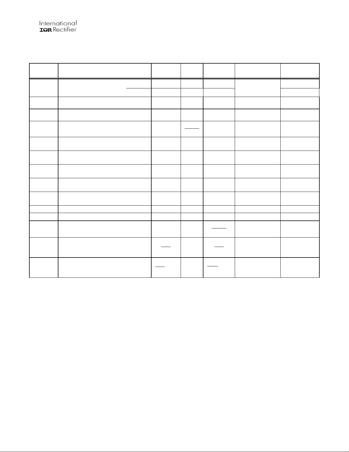
Product Summary
V
(max) IR2277 1200 V
OFFSET
IR2177 600 V
V
range ±250mV
in
Bootstrap supply range 8-20 V
Floating channel quiescent
current (max)
Sensing latency (max) 7.5 µsec
Throughput 40ksample/sec
Over Current threshold
(max)
2.2 mA
(@20kHz)
(@20kHz)
±470 mV
Package
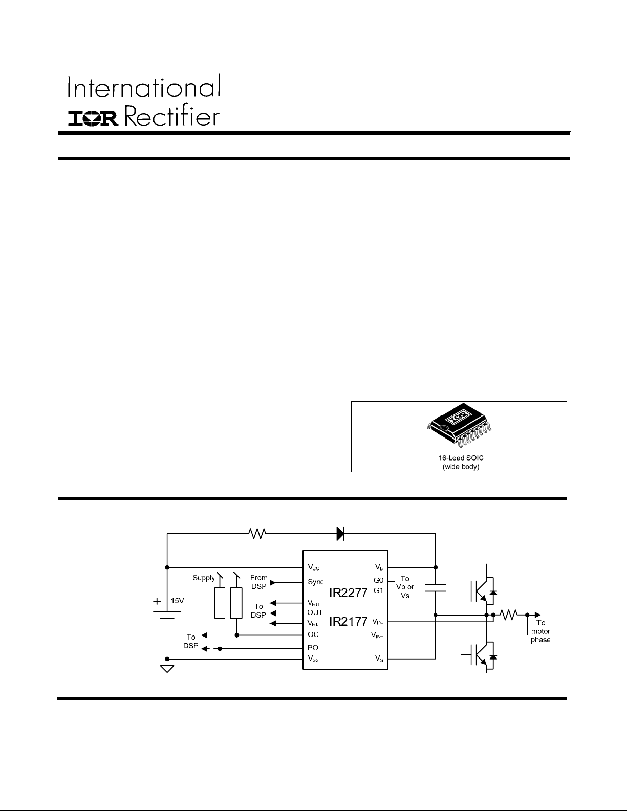
Typical Connection
(Please refer to
Lead Assignments
for correct pin
configuration. This
diagram shows
electrical
connections only)
1 www.irf.com
Page 2
IR2277S/IR2177S(PbF)
Absolute Maximum Ratings
Absolute Maximum Ratings indicate sustained limits beyond which damage to the device may occur. All voltage parameters
are absolute voltages referenced to V
Dissipation ratings are measured under board mounted and still air conditions.
, all currents are defined positive into any lead. The Thermal Resistance and Power
SS
Symbol Definition Min. Max. Units
VB High Side Floating Supply Voltage
VS High Side Floating Ground Voltage
V
/ V
in+
High-Side Inputs Voltages
in-
G0 / G1 High-Side Range Selectors
VCC Low-Side Fixed Supply Voltage - 0.3 25 V
Sync Low-Side Input Synchronization Signal
VRH/VRL DSP Reference Hi gh and Low Voltages - 0.3 VCC + 0.3 V
Out Analog Output Voltage - 0.3 VCC + 0.3 V
PO PWM Output - 0.3 VCC + 0.3 V
OC Over Current Output Voltage - 0.3 VCC + 0.3 V
dVS/dt Allowable Offset Voltage Slew Rate 50 V/ns
PD Maximum Power Dissipation 250 mW
R
Thermal Resistance, Junction to Ambient 90 ºC/W
thJA
TJ Junction Temperature -40 125 ºC
TS Storage Temperature -55 150 ºC
TL Lead Temperature (Soldering, 10 seconds) 300 ºC
IR2277 - 0.3 1225
V
V
- 25
B
- 5
S
- 0.3
S
625
+ 0.3 V
V
B
+ 0.3 V
V
B
+ 0.3 V
V
B
IR2177 - 0.3
V
- 0.3 VCC + 0.3 V
V
Recommended Operating Conditions
For proper operation the device should be used within the recommended conditions. All voltage p arameters are absolute
voltages referenced to V
. The
ss
Symbol
VBS High Side Floating Supply Voltage (V
VS
V
/ V
in+
G0 / G1 High-Side Range Selectors Note 1 Note1
VCC Low Side Logic Fixed Supply Voltage 8 20 V
Sync Low-Side Input Synchronization Signal
f
sync
PO PWM Output -0.3 Note 2 V
OC Over Current Output Voltage -0.3 Note 2 V
VRH
VRL
TA
Note 1: Shorted to VS or V
Note 2: Pull-Up Resistor to
High Side Floating Ground Voltage
High-Side Inputs Voltages VS - 5.0 VS + 5.0 V
in-
Sync Input Frequency
OUT Reference High Voltage 3 V
OUT Reference Low Voltage V
Ambient Temperature -40 125 ºC
B
V
CC
offset rating is tested with all supplies biased at 15V differential.
V
s
Definition Min. Max. Units
V
)
V
-
B
S
IR2277 1200
IR2177
Using PO 4 20
Using OUT 8 20
+ 8.0 VS + 20 V
S
VSS V
-5
V
SS
600
V
CC
-2.5 V
CC
-3 V
RH
V
kHz
2 www.irf.com
Page 3
IR2277S/IR2177S(PbF)
Static Electrical Characteristics
, VBS = 15V unless otherwise specified. Temp=27°C; Vin=V
V
CC
Pin: V
, VSS, VB, VS
CC
Symbol Definition Min. Typ. Max. Units
I
Quiescent VBS supply current 1 2.2 mA
QBS
I
Quiescent VCC supply current 6 mA
QCC
IR2277 50
ILK Offset supply leakage current
IR2177 50
Pin: V
in+
, V
, Sync, G0, G1, OC
in-
Symbol Definition Min. Typ. Max. Units
V
Maximum input voltage before saturation 250 mV
inmax
V
Minimum input voltage before saturation -250 mV
inmin
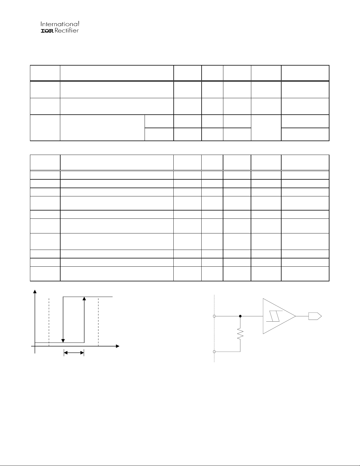
VIH Sync Input High threshold 2.2 V See Figure 1
VIL Sync Input Low threshold 0.8
Vhy Sync Input Hysteresis 0.2 V See Figure 1
I
V
vinp
Ipu G0, G1 pull-up Current -20 -8 µA
|V
|
octh
R
Sync
R
Over Current On Resistance 25 75
onOC
input current -18 -6 µA
in+
Over Current Activation Threshold 300 470 mV
SYNC to VSS internal pull-down 6 12
- Vin.
in+
µA
V
kΩ
Ω
Test
Conditions
f
= 10kHz,
sync
20kHz
f
= 10kHz,
sync
20kHz
V
= VS =
B
1200V
= VS = 600V
V
B
Test
Conditions
See Figure 1
f
= 4kHz to
sync
20kHz
G1, G0 = V
5V
@ I = 2mA
Figure
See
B
3
-
Schm itt trig g e r
SYNC
R
sync
V
IL
V
hy
V
IH
V
SS
Figure 1: Sync input thresholds Figure 2: Sync input circuit
Page 4
IR2277S/IR2177S(PbF)
j
Pin: PO
Symbol Definition Min. Typ. Max. Units
V
POs
∆V
POs
∆T
∆V
POs
Gp PWM Output Gain -38 -40.5 -42.5 %/V Vin=±250mV
∆G
/
p
CMRR
PO
V
POlin
∆ V
lin
V
thPO
PSRR PO PSRR for PO Output 0.2 %/V
R
onPO
Note1: Refer to PO output description for channels definition
Input offset voltage measured by PWM
output
/
Input offset voltage temperature drift TBD
-50 20 mV
µV/°C
∆offset between samples on channel1
and channel2 measured at PO (See
-10 10 mV
Note1)
∆Tj
PWM Output Gain Temperature Drift TBD %/(V
PO Output common mode (V
) rejection 0.2 m%/V
S
ºC)
*
PO Linearity 0.07 0.2 % 10kHz
∆Tj
PO Linearity Temperature Drift TBD %/ºC 10kHz
/
PO threshold for OC reset 0.8 1.6 V
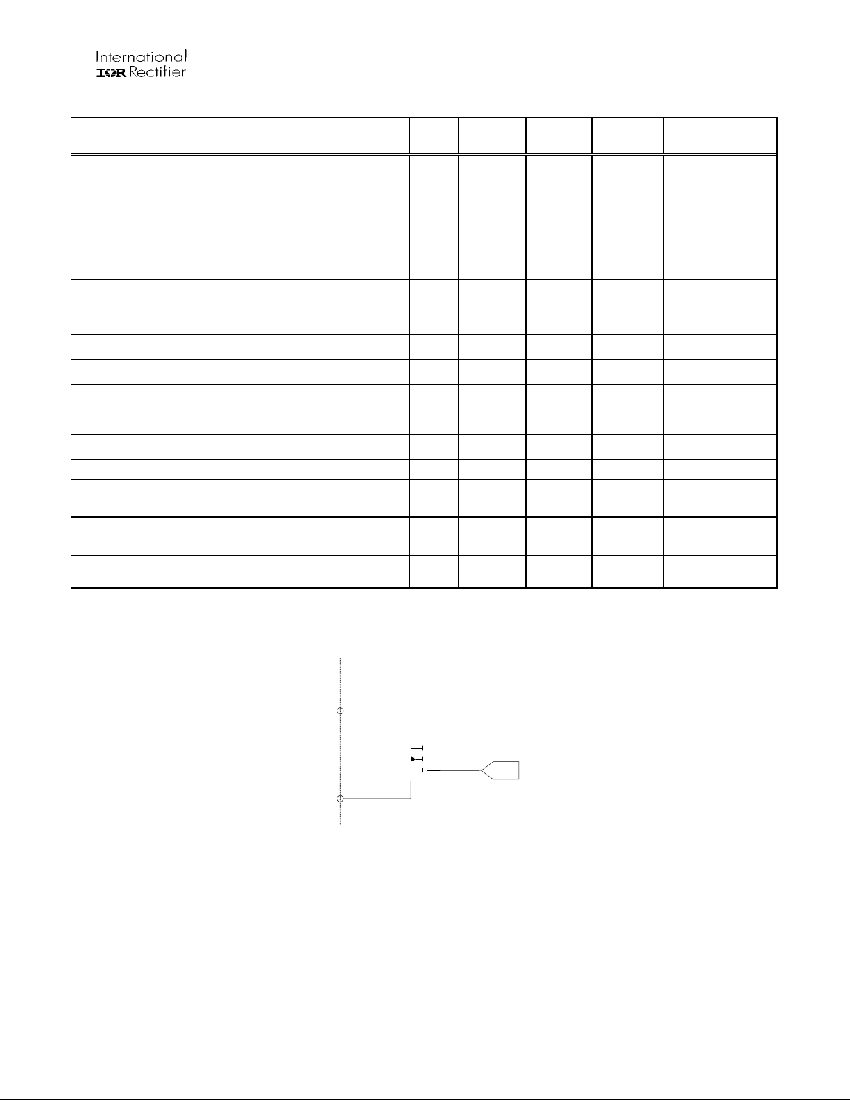
PO On Resistance 25 75
Ω
Test
Conditions
R
=500 Ω
pull-up
= 4, 20kHz
f
sync
V
Ext supply=5V
(See Figure 6)
OC active (See
V
=2.75V
threshold
f
= 10kHz
sync
See Figure 6
= 0,
V
s-Vss
600V
f
= 10kHz
sync
Figure 4
CC=VBS
)
=
8,20V
@ I = 2mA
See Figure 3
PO
or
OC
R
ON
V
SS
Figure 3: PO and OC open collector circuit
4 www.irf.com
Internal signal
Page 5

IR2277S/IR2177S(PbF)
Pin: OUT, VRH, VRL
Symbol Definition Min. Typ. Max. Units
R
V
REF
V
aos
∆ V
/
aos
∆Tj
∆V
aos
to VRL input resistance 36 84
RH
Input offset voltage measured by
analog output
-100 50 mV
kΩ
Input offset voltage temperature drift TBD µV / ºC
∆offset between samples on channel1
and channel2 measured at OUT
(Note1)
Test
Conditions
f
= 8kHz, 20
sync
kHz
Measured by
analog output
f
= 8kHz, 20
sync
kHz
Ga Analog Output Gain -20% 2VR +20% V/V
-1
∆Ga / ∆Tj
CMRR
OUT
V
OUTlin
∆ V
/
lin
∆Tj
PSRR
OUT
V
Vout Low Saturation 0 50 mV Vin= -500mV
OUTl
V
OUTh
Note1: Refer to PO output description for channels definition
Analog Output Gain Temperature Drift TBD ºC
Analog Output common mode (VS
offset) rejection
100 dB
Out Linearity 0.3 0.7 %
Out Linearity Temperature Drift TBD %/ºC
PSRR for Analog Output 30 100 dB
Vout High Saturation VRH+0.2 VRH+0.7 V Vin = +500mV
VR=VRH-VRL=3V
Vs-Vss=0V,
f
sync
f
sync
f
sync
V
CC
600V
= 10kHz
= 8kHz,
20kHz
= 8kHz,
20kHz
= VBS =8V,
20V
5 www.irf.com
Page 6
IR2277S/IR2177S(PbF)
AC Electrical Characteristics
V
V
BIAS
Symbol Definition Min. Typ. Max. Units
f
sync
f
out
BW Bandwidth (@ -3 dB)
GD Group Delay (input filter)
, VBS) = 15V unless otherwise specified. Temp=27°C.
(
CC
PWM frequency
PO 4
OUT 8
Throughput
Test
Conditions
f2⋅
sync
f
sync
1
f4
⋅
sync
20
kHz
20
ksample/sec
kHz
µs
D
min
D
max
t
dOCon
T
OCoff
C
Analog output load capacitor 0 50 nF NOTE 2
load
SL
OUT
t
Output settling time (1%) 5 30 µs
settl
MD Measure Delay
SR
SR
OUT
Note 1: negative logic, see Figure 4 on page 7
Note 2: Cload < 5 nF avoids overshoot
Minimum Duty Cycle (Note 1) 10 % Vin=+V
Maximum Duty Cycle (Note 1) 30 % Vin=-V
De-bounce time of OC 2.7 3.5 4.7 µs See Figure 4
Time to reset OC forcing PO 0.5 µs
Analog output (OUT) Slew Rate 0.2 1 V/µs
Step response (max time to reach
steady state) for PO output
Step response (max time to reach
steady state) for OUT output
30.0
f2
⋅
sync
51.0
f
sync
51.0
t+
settl
f
sync
3.1
f
sync
3.1
t+
sync
settl
f
µs
µs
µs
See
See
Figure 5
See
Figure 5
C
out
C
out
inmax
inmin
Figure
≤ 5 nF
≤ 5 nF
4
6 www.irf.com
Page 7

IR2277S/IR2177S(PbF)
Figure 4: OC timing diagram
V
max
V
in
V
min
SYNC
PO
V
RH
OUT
V
RL
SR
(PO full response time)
MD
t
settl
SR
OUT
OUT full response time
(
Figure 5: timing diagram
)
7 www.irf.com
Page 8

V
max
Vin
V
min
SYNC
IR2277S/IR2177S(PbF)
Supply=5V
PO
GP *V
POs1
20% 20%
GP *V
POs0
DV
POs
GP *V
POs1
20% 20%
= V
POs1-VPOs0
GP *V
Vth=2.75V
POs0
Figure 6: ∆offset between two consecutive samples measured at PO
8 www.irf.com
Page 9

Lead Assignments
IR2277S/IR2177S(PbF)
SOIC16WB
Lead Definitions
Pin Symbol Description
1 VCC
2 OUT
3 VSS
4 VRL
5 VRH
6 OC
7 PO
8 Sync
9 NC
10 NC
11 G0
12 G1
13 VS
14 V
15 V
16 VB
IN-
IN+
Low side voltage supply
Analog output
Low side ground supply
Lower rail of A/D voltage range
Higher rail of A/D voltage range
Over current signal (open drain)
PWM output (open drain)
DSP synchronization signal
No connection
No connection
Integrator gain lsb
Integrator gain msb
High side return
Negative sense input
Positive sense input
High side supply
9 www.irf.com
Page 10

IR2277S/IR2177S(PbF)
Timing and logic state diagrams description
** See OC and PO detailed descriptions below in this document
Functional block diagram
10 www.irf.com
Page 11

IR2277S/IR2177S(PbF)
τ
1 Device Description
1.1 SYNC input
Sync input clocks the whole device. In order to
make the device work properly it must be
synchronous with the triangular PWM carrier as
shown in Figure 8.
SYNC pin is internally pulled-down (10 kΩ) to V
1.2 PWM Output (PO)
PWM output is an open collector output (active low).
It must be pulled-up to proper supply with an
external resistor (suggested value between 500Ω
and 10kΩ).
Supply
V
low
Figure 7: PO rising and falling slopes
PO pull-up resistor determines the rising slope of
the PO output and the lower value of PO as shown
in Figure 7, where
capacitance and R is the pull-up resistance.
low
SupplyV
⋅=
where R
and R
is the internal open collector resistance
on
is the external pull-up resistance.
pull-up
PO duty cycle is defined for active low logic by the
following formula:
T
D
Eq. 1
PO duty cycle (D
Zero input voltage corresponds to 20% duty cycle.
=
n
T
n
τ
RC=
, C is the total PO pin
R
on
RR
+
uppullon
−
ncycleoff
1__ +
ncycle
_
) swings between 10% and 30%.
SS
.
A residual offset can be read in PO duty cycle
according to V
(see Static electrical
POs
characteristics).
According to
Figure 8, it can be assumed that odd cycles are
represented by SYNC at high level (let’s name
channel 1 the output related to this state of SYNC)
and even cycles represented by SYNC at low level
(channel 2).
The two channels are independent in order to
provide the correct duty cycle value of PO even for
non-50% duty cycle of SYNC signal. Small variation
of SYNC duty cycle are then allowed and
automatically corrected when calculating the duty
cycle using Eq. 1.
However, channel 1 and channel 2 can have a
difference in offset value which is specified in
∆V
(see Static electrical characteristics).
POS
To implement a correct offset compensation of PO
duty cycle and analog OUT, each channel must be
compensated separately.
1.3 Over Current output (OC)
OC output is an open drain pin (active low).
A simplified block diagram of the over current circuit
is shown in the
Figure 9.
Over current is detected when |V
If an event of over current lasts longer than t
OC pin is forced to V
and remains latched until
SS
PO is externally forced low for at least t
timing on Figure 4). During an over current event
(OC is low), PO is off (pulled-up by external
resistor).
If OC is reset by PO and over current is still active,
OC pin will be forced low again by the next edge of
SYNC signal.
To reset OC state PO must be forced to V
least T
OCoff
.
• Autoreset function
The autoreset function consists in clearing
automatically the OC fault.
To enable the autoreset function, simply short
circuit the OC pin with the PO pin.
|=|V
in
inp-Vinm
|>V
OCoff
SS
OCth
dOCon
(see
for at
.
,
11 www.irf.com
Page 12

Triangular
SYNC (0)
PO
IR2277S/IR2177S(PbF)
Cycle 1 Cycle 2 Cycle 3 Cycle 4
T
off_cycle1
Dn =
1
T
cycle1
T
cycleoff
2_
T
cycle
1
Dn =
T
off_cycle2
T
cycle2
T
cycleoff
T
cycle
3_
2
2
T
off_cycle3
Dn =
3
T
cycle3
T
T
cycleoff
cycle
T
off_cycle4
4_
3
Figure 8: PO Duty Cycle
Ext
supply
High voltage
V
IN+
V
IN-
Over current
detection
Low voltage
SRD
OC
V
SS
Level shifter
PO
Figure 9: Over current block diagram
12 www.irf.com
Page 13

IR2277S/IR2177S(PbF)
∆
1.4 Analog Output (OUT)
The analog output is internally buffered and capable
of driving capacitive loads ranging up to 50nF.
V
and VRL set the dynamic range and gain of OUT
RH
pin.
Additional circuitry to protect A/D converter input
against excessive voltage is not required.
Hereafter follow some definitions (see Figure 10
and following).
• V
in=Vinp-Vinm
• Input referred analog offset (V
): It is
aos
the input that gives an output that equals
VV
+
RLRH
OUT
=
(referred to VSS).
2
1
SYNC
OUT
=
a
V
∆
in
curve
in
.
++≤≤++
• Gain: It is defined by the ratio G
• Linearity: It is defined by the maximum
difference between the ideal OUT/V
and the measured curve depurated of the
offset voltage and the gain error.
The analog output is also defined by some dynamic
characteristics (see figure 8):
• Slew Rate (SL
). The maximum slope of
OUT
OUT measured in V/µs
• Settling time (t
). Time needed by the
settl
analog output (OUT) to reach 90% of final
value.
• Measure delay (MD). It is defined by the
time interval between the actual SYNC
edge and PO rising edge.
• Step response (SR). Is the time needed by
Output to reach the final value after a step
of the input.
Is always within the following range:
1
f
⋅
2
SYNC
settl
SROUTtMD
f
tMD
settl
V
V
V
V
V
V
V
V
V
OUT
RH
VRH+V
RL
2
RL
SS
V
aos
Figure 10: Input offset definition
OUT
RH
G
RL
SS
a
G
V
id
in
Figure 11: Gain definition
OUT
RH
G
a
G
RL
SS
id
(V
if PO is measured
pos
instead of OUT)
OUT
Linearity
Error
V
V
V
in
in
in
Figure 12: Linearity error definition
13 www.irf.com
Page 14

IR2277S/IR2177S(PbF)
+
−
1.5 DC transfer functions
The working principle of the device can be easily
explained by Figure 13, in which the main signals
are represented.
Triangular
reference
SYNC
Vin
PO
VRH
OUT
VRL
Figure 13: Main current sensor signals and
outputs
PWM out (PO pin) gives a duty cycle which is
inversely proportional to the input signal while the
OUT pin gives the analog converted output.
Eq. 2 gives the resulting D
pin):
Eq. 2
D ⋅−=
40%20
where V
= V
in
inp-Vinm
of the PWM output (PO
n
%
V
inn
V
VV
Eq. 3
()
2
+⋅−⋅=
VVVOUT
inRLRH
RLRH
2
The same equation can be referred to V
RL
, as
follows in Eq. 4:
Eq. 4
VV
()
2
OUT
-250mV
-200mV
-100mV
Figure 15: ideal OUT/V
VVVVOUT
+⋅−⋅=−
inRLRHRL
V
RH
(VRH+VRL)/2
V
RL
0mV
100mV
transfer function
in
2
V
250mV
200mV
RLRH
in
PO duty cycle
30%
25%
20%
15%
V
10%
in
Figure 14: PO Duty Cycle (D
)
n
The Voltage-to-Time conver si on (V
to PO) must be
in
reconstructed (see Functional Block Diagram) to
give an analog voltage output at OUT pin.
OUT pin swings from V
output (referred to V
SS
to VRH, so the analog
RL
) follows Eq. 3:
14 www.irf.com
Page 15

IR2277S/IR2177S(PbF)
Filter AC characteristic
IR2177/2277 signal path can be considered as
composed by three stages in series (see Figure 17).
The first two stages perform the filtering action.
Stage 1 (input filter) implements the filtering action
originating the transfer function shown in Figure 18.
The input filter is a self-adaptive reset integrator
which performs an accurate ripple cancellation. This
stage extracts automatically the PWM frequency
from Sync signal and puts transmission zeros at
even harmonics, rejecting the unwanted PWM
noise.
The following timing diagram shows the principle by
which even harmonics are rejected (Figure 16).
As can be seen from Figure 18, the odd harmonics
are rejected as a first order low pass filter with a
single pole placed in f
PWM
.
The input filter group delay in the pass-band is very
low (see GD on AC electrical characteristics) due to
the beneficial action of the zeroes.
The second stage samples the result of the first
stage at double Sync frequency. This action can be
used to fully remove the odd harmonics from the
input signal.
To perform this cancellation it is necessary a shift of
90 degrees of the SYNC signal with respect to the
triangular carrier edges (SYNC2).
The following timing diagrams show the principle of
odd harmonics cancellation (Figure 19), in which
SYNC2 allows the sampling of stage 1 output
during odd harmonic zero crossings.
Odd harmonic cancellation using SYNC2 (i.e. 90
degree shifted SYNC signal) signal will introduce
Tsync/4 additional propagation delay.
Anther way to obtain the same result (odd
harmonics cancellation) can be achieved by
controller computing the average of two consecutive
PO results using SYNC1 (SYNC is in this case
aligned to triangular edges, i.e. 0 degree shift).
This method is suitable for most symmetric (center
aligned) PWM schemes.
For this particular PWM scheme another suitable
solution is driving the IR2x77 with a half frequency
SYNC signal (f
sync=fPWM
/2).
In this case the cut frequency of the input filter is
reduced by half allowing zeroes to be put at f
PWM
multiples (i.e. even and odd harmonics cancellation,
no more computational effort needed by the
controller).
Figure 16: Even harmonic cancellation principle
Figure 17: Simplified block diagram
15 www.irf.com
Page 16

IR2277S/IR2177S(PbF)
Figure 18: Input filter transfer function (10 kHz PWM)
16 www.irf.com
Page 17

IR2277S/IR2177S(PbF)
Switching level
Switching level
Triangular
Triangular
Phase voltage
Phase voltage
Phase current
Phase current
Current Mean
Current Mean
Fundamental
Fundamental
harmonic
harmonic
Third
Third
harmonic
harmonic
Fundamental
Fundamental
harmonic
harmonic
Third
Third
harmonic
harmonic
SYNC 1
SYNC 1
Error
Error
SYNC 2
SYNC 2
Stage 1 input:
Input signal
components
st
(1
and 2
harmonic only)
Stage 1
output
Sampling
Sampling
instant
instant
Sampling
Sampling
instant
instant
nd
Figure 19: Even harmonic cancellation principle
1.6 Input filter gain setting
G0 and G1 pins are used to change the time
constant of the integrators of the high side input
filter.
To avoid internal saturation of the input filter, G0
and G1 must be connect according to SYNC
frequency as shown in Table 1. A too small time
constant may saturate the internal integrator, while
a large time constant may reduce accuracy.
G0 and G1 do not affect the overall current sensor
gain.
f
G0 G1
PWM
> 16 kHz * VB VB
16 / 10 kHz VS VB
10 / 6 kHz VB VS
< 6 kHz VS VS
*Æ 40 kHz
Table 1: G0, G1 gain settings
2 Sizing tips
2.1 Bootstrap supply
The V
side drivers circuitry of the IR2277S/IR2177S. V
supply sit on top of the V
floating.
The bootstrap method to generate V
be used with IR2277S/IR2177S current sensors.
The bootstrap supply is formed by a diode and a
capacitor connected as in Figure 20.
voltage provides the supply to the high
BS1,2,3
voltage and so it must be
S
supply can
BS
IR2277SorIR2177S
17 www.irf.com
Figure 20: bootstrap supply schematic
BS
Page 18

IR2277S/IR2177S(PbF)
⋅
=
=
This method has the advantage of being simple and
low cost but may force some limitations on dutycycle and on-time since they are limited by the
requirement to refresh the charge in the bootstrap
capacitor.
Proper capacitor choice can reduce drastically
these limitations.
Bootstrap capacitor sizing
Given the maximum admitted voltage drop for VBS,
namely ∆V
V
decrease are:
BS
, the influencing factors contributing to
BS
− Floating section quiescent current (I
− Floating section leakage current (I
− Bootstrap diode leakage current (I
);
QBS
)
LK
LK_DIODE
);
− Charge required by the internal level shifters
); typical 20nC
(Q
LS
− Bootstrap capacitor leakage current (I
− High side on time (T
I
is only relevant when using an electrolytic
LK_CAP
HON
).
LK_CAP
);
capacitor and can be ignored if other types of
capacitors are used. It is strongly recommend using
at least one low ESR ceramic capacitor (paralleling
electrolytic and low ESR ceramic may result in an
efficient solution).
Then we have:
+++++= )(
TIIIIQQ
__
HONCAPLKDIODELKLKQBSLSTOT
The minimum size of bootstrap capacitor is then:
Q
TOT
C
BOOT
min
=
V
∆
BS
Some important considerations
a) Voltage ripple
There are three different cases making the
bootstrap circuit get conductive (see Figure 20)
I
IGBT displaying relevant V
In this case we have the lowest value for V
This represents the worst case for the bootstrap
capacitor sizing. When the IGBT is turned off the
Vs node is pushed up by the load current until the
< 0; the load current flows in the low side
LOAD
CEon
VVVV −−=
CEonFCCBS
BS
.
high side freewheeling diode get forwarded
biased
I
on and V
= 0; the IGBT is not loaded while being
LOAD
can be neglected
CE
VVV −
FCCBS
I
> 0; the load current flows through the
LOAD
freewheeling diode
VVVV +−
FPFCCBS
In this case we have the highest value for V
Turning on the high side IGBT, I
and V
is pulled up.
S
flows into it
LOAD
BS
.
b) Bootstrap Resistor
A resistor (R
boot
) is placed in series with the
bootstrap diode (see Figure 20) to limit the current
when the bootstrap capacitor is initially charged. We
suggest not exceeding some Ohms (typically 5,
maximum 10 Ohms) to avoid increasing the V
BS
time-constant. The minimum on time for charging
the bootstrap capacitor or for refreshing its charge
must be verified against this time-constant.
c) Bootstrap Capacitor
For high T
designs where an electrolytic tank
HON
capacitor is used, its ESR must be considered. This
parasitic resistance develops a voltage divider with
R
generating a voltage step on V
boot
at the first
BS
charge of bootstrap capacitor. The voltage step and
the related speed (dV
/dt) should be limited. As a
BS
general rule, ESR should meet the following
constraint:
ESR
+
RESR
BOOT
CC
VV
3≤⋅
Parallel combination of small ceramic and large
electrolytic capacitors is normally the best
compromise, the first acting as fast charge tank for
the gate charge only and limiting the dV
/dt by
BS
reducing the equivalent resistance while the second
keeps the V
voltage drop inside the desired ∆VBS.
BS
d) Bootstrap Diode
The diode must have a BV> 600V (or 1200V
depending on application) and a fast recovery time
(t
< 100 ns) to minimize the amount of charge fed
rr
back from the bootstrap capacitor to V
supply.
CC
18 www.irf.com
Page 19

IR2277S/IR2177S(PbF)
3 PCB LAYOUT TIPS
3.1 Distance from H to L voltage
The IR2277S/IR2177S package (wide body)
maximizes the distance between floating (from DCto DC+) and low voltage pins (V
). It is strongly
SS
recommended to place components tied to floating
voltage in the respective high voltage portions of the
device (V
, VS) side.
B
3.2 Ground plane
Ground plane must NOT be placed under or nearby
the high voltage floating side to minimize noise
coupling.
VB
VS
Vin-
Vin+
Antenna
Loop
Figure 21: antenna loops
3.3 Antenna loops and inputs
connection
Current loops behave like antennas able to receive
EM noise. In order to reduce EM coupling loops
must be reduced as much as possible. Figure 21
shows the high side shunt loops.
Moreover it is strongly suggested to use Kelvin
connections for V
connect V
to V
S
and V
in+
close to the shunt resistor as
in-
to shunt paths and star-
in-
explained in Fig. 22.
VB
VS
Vin-
Vin+
Figure 22: Recommended shunt connection
3.4 Supply capacitors
The supply capacitors must be placed as close as
possible to the device pins (V
ground tied supply, V
and VS for the floating
B
supply) in order to minimize parasitic traces
inductance/resistance
and VSS for the
CC
19 www.irf.com
Page 20

Case Outline
IR2277S/IR2177S(PbF)
WORLD HEADQUARTERS: 233 Kansas St., El Segundo, California 90245 Tel: (310) 252-7105
Data and specifications subject to change without notice. 8/18/2005
20 www.irf.com
This part has been qualified for the Industrial Market
 Loading...