

Page 1
Data Sheet No. PD60208 Rev. E
IR2175(S) & (PbF)
LINEAR CURRENT SENSING IC
Features
• Floating channel up to +600V
• Monolithic integration
• Linear current feedback through shunt resistor
• Direct digital PWM output for easy interface
•
•
•
•
condition
•
•
QBS
Low I
Independent fast overcurrent trip signal
High common mode noise immunity
Input overvoltage protection for IGBT short circuit
Open Drain outputs
Also available LEAD-FREE
allows the boot strap power supply
Description
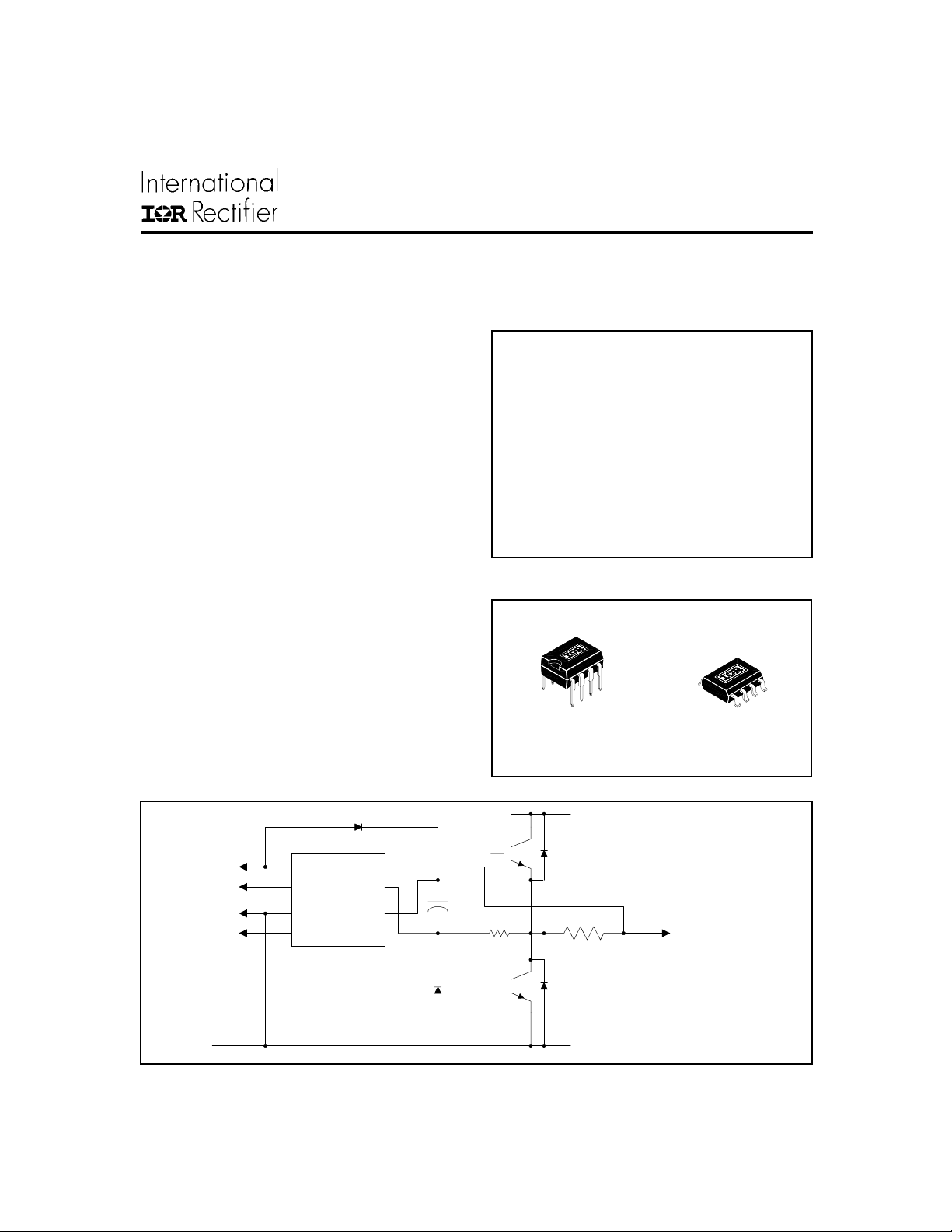
The IR2175 is a monolithic current sensing IC designed
for motor drive applications. It senses the motor phase
current through an external shunt resistor, converts from
analog to digital signal, and transfers the signal to the
low side. IR’s proprietary high voltage isolation technology is implemented to enable the high bandwidth
signal processing. The output format is discrete PWM
to eliminate need for the A/D input interface for the
IR2175. The dedicated overcurrent trip (OC) signal facilitates IGBT short circuit protection. The open-drain
outputs make easy for any interface from 3.3V to 15V. S
Product Summary
V
OFFSET
I
QBS
V
in
Gain temp.drift 20ppm/
f
o
Overcurrent trip 2µsec (typ)
signal delay
Overcurrent trip level +/-260mV (typ.)
600Vmax
2mA
+/-260mVmax
o
C (typ.)
130kHz (typ.)
Packages
8 Lead PDIP
IR2175
8 Lead SOIC
IR2175S
Block Diagram
15V
PWM Output
GND
VCC
PO
COM
OCOvercurrent
Up to 600V
V+
VS
IR2175
VB
To Motor Phase
(Refer to Lead Assignments for correct pin configuration). This/These
diagram(s) show electrical connections only. Please refer to our Application Notes and DesignTips for
proper circuit board layout.
Page 2
IR2175
(S) & (PbF)
Absolute Maximum Ratings
Absolute maximum ratings indicate sustained limits beyond which damage to the device may occur. All voltage
parameters are absolute voltages referenced to COM, all currents are defined positive into any lead. The thermal
resistance and power dissipation ratings are measured under board mounted and still air conditions.
Symbol Definition Min. Max. Units
V
S
V
BS
V
CC
V
IN
V
PO
V
OC
dV/dt Allowable offset voltage slew rate — 50 V/ns
P
D
Rth
JA
T
J
T
S
T
L
Note 1: Capacitors are required between VB and Vs when bootstrap power is used. The external power supply,
when used, is required between VB and Vs pins.
High side offset voltage -0.3 600
High side floating supply voltage
Low side and logic fixed supply voltage -0.3 25
Maximum input voltage between V
Digital PWM output voltage COM -0.3 VCC +0.3
Overcurrent output voltage COM -0.3 VCC +0.3
Package power dissipation @ T
Thermal resistance, junction to ambient 8 lead SOIC — 200
Junction temperature — 150
Storage temperature -55 150
Lead temperature (soldering, 10 seconds) — 300
IN+ and VS
≤ +25°C 8 lead SOIC — .625
A
8 lead PDIP — 1.0
8 lead PDIP — 125
-0.3 25
-5 5
V
W
°C/W
°C
Recommended Operating Conditions
The output logic timing diagram is shown in figure 1. For proper operation the device should be used within the recommended
conditions.
Symbol Definition Min. Max. Units
V
B
V
S
V
PO
V
OC
V
CC
V
IN
T
A
2
High side floating supply voltage VS +13.0 VS +20
High side floating supply offset voltage 0.3 600
Digital PWM output voltage COM VCC
Overcurrent output voltage COM VCC
Low side and logic fixed supply voltage 9.5 20
Input voltage between V
Ambient temperature -40 125
IN+
and V
S
-260 +260 mV
V
°C
www.irf.com
Page 3
IR2175
(S) & (PbF)
DC Electrical Characteristics
V
= VBS = 15V, and T
CC
Symbol Definition Min. Typ. Max. Units Test Conditions
V
IN
V
OC+
V
OC-
V
OS
∆
V
OS
G Gain (duty cycle % per VIN) 155 160 165 %/V max gain error=5%
∆
∆
G
/
I
LK
I
QBS
I
QCC
LIN Linearity (duty cycle deviation from ideal linearity — 0.5 1 %
∆
V
LIN
I
OPO
I
OCC
Note 1: ±10mV offset represents ±1.5% duty cycle fluctuation
Note 2: Gain = (full range of duty cycle in %) / (full input voltage range).
Nominal input voltage range before saturation -260 — 260
V
IN+
Overcurrent trip positive input voltage —
Overcurrent trip negative input voltage — -260 —
Input offset voltage -10 0 10 VIN = 0V (Note 1)
∆
/
T
/
Input offset voltage temperature drift — 25 — µV/
A
T
Gain temperature drift — 20 — ppm/oC
A
Offset supply leakage current — — 50 µA V
Quiescent VBS supply current — 2 — VS = 0V
Quiescent VCC supply current — — 0.5
curve)
∆
Linearity temperature drift — .005 — %/oC
A
T
Digital PWM output sink current 20 — —
OC output sink current 10 — —
= 25o unless otherwise specified.
A
_
V
S
260
2——
1——
—
mV
mA
mA
o
C
(Note 2)
= VS = 600V
B
VO = 1V
VO = 0.1V
VO = 1V
VO = 0.1V
AC Electrical Characteristics
VCC = VBS = 15V, and T
Symbol Definition Min. Typ. Max. Units Test Conditions
Propagation delay characteristics
fo Carrier frequency output 100 130 180 kHz
∆
∆
f
/
Dmin Minimum duty — 9 — %
Dmax Maximum duty — 91 — % V
BW fo bandwidth — 15 — kHz
PHS Phase shift at 1kHz — -10 —
tdoc Propagation delay time of OC 1 2 —
twoc Low true pulse width of OC — 1.5 —
Temperature drift of carrier frequency — 500 — ppm/oC
A
T
www.irf.com
= 25o unless otherwise specified.
A
VIN = 0 & 5V
V
+ = 100mVpk -pk
IN
sine wave, gain=-3dB
o
VIN+ =100mVpk-pk
µsec
figure 1
VIN+=-260mV,
+=+260mV
IN
sine wave
3
Page 4

IR2175
(S) & (PbF)
Timing Waveforms
PO
PO
Duty=9%
Vin+= -260mV
Vs = 0V
Duty=91%
Vin+= +260mV
Vs = 0V
Carrier Frequency =
130kHz
Figure 1 Output waveform
Application Hint:
T emperature drift of the output carrier frequency can be cancelled by measuring both a PWM period and the on-time
of PWM (Duty) at the same time. Since both periods vary in the same direction, computing the ratio between these
values at each PWM period gives consistent measurement of the current feedback over the temperature drift.
4
www.irf.com
Page 5

Lead Definitions
Symbol Description
V
CC
COM Low side logic ground
V
IN+
V
B
V
S
PO Digital PWM output
OC
N.C. No connection
Low side and logic supply voltage
Positive sense input
High side supply
High side return
Overcurrent output (negative logic)
Lead Assignment
IR2175
(S) & (PbF)
www.irf.com
VC
1
C
2
PO
3
COM
4
OC
VIN
Vs
NC
8
+
7
V
6
B
5
8 lead SOIC
Also available LEAD-FREE (PbF)
IR2175S
VC
1
C
2
PO
3
COM
4
OC
VIN
+
Vs
V
B
NC
8 lead PDIP
Also available LEAD-FREE (PbF)
IR2175
8
7
6
5
5
Page 6

IR2175
(S) & (PbF)
Case Outlines
A
E
D B
5
87
6
6X
0.25 [ . 010 ]
65
H
4312
0.25 [ . 010 ] A
e
8X b
e1
A1
A
CAB
NOTES:
1. DIMENSIONING & TOLERANCING PER ASME Y14.5M-1994.
2. CONT ROLLING DIMENSION: MILL IMETER
3. D IMENSI ONS A RE SHOWN IN MILLIMETERS [INCHES].
4. OUTLI NE CONFORMS T O JED EC OUT L INE MS-012AA.
C
0.10 [ . 004 ]
8 Lead PDIP
6.46 [. 2 55]
3X 1.27 [. 05 0]
y
8 Lead SOIC
01-3003 01
DIM
FOOTPRINT
8X 0.72 [. 02 8]
8X 1.78 [. 07 0]
MIN MAX
A
.0532
A1
b
c .0075 .0098 0.19 0.25
D
E
e
e1
H
K
L
y
.0688
.0040
.0098
.013
.020
.189
.1968
.1497
.1574
.050 BASIC
.025 BASIC 0.635 BASI C
.2284
.2440
.0099
.0196
.016
.050
0°
K x 4 5°
8X L
8X c
7
5 DIMENSI ON D OES NOT INCLUDE MOLD PROTR USIONS.
MOLD PROTRUSIONS NOT TO EXC EED 0.15 [.006].
6 DIMENSI ON D OES NOT INCLUDE MOLD PROTR USIONS.
MOLD PROTRUSIONS NOT TO EXC EED 0.25 [.010].
7 DIMENSI ON IS THE LENGT H OF LEAD FOR SOLD ERING TO
A SUBSTRATE.
01-0021 11
8°
01-6014
(MS-001AB)
MILLIMETERSINC H E S
MIN MAX
1.35
1.75
0.10
0.25
0.33
0.51
4.80
5.00
3.80
4.00
1.27 BASIC
5.80
6.20
0.25
0.50
0.40
1.27
8°
0°
01-6027
(MS-012AA)
6
www.irf.com
Page 7

IR2175
LEADFREE PART MARKING INFORMATION
(S) & (PbF)
Part number
Date code
Pin 1
Identifier
?
MARKING CODE
Lead Free Released
P
Non-Lead Free
Released
IRxxxxxx
YWW?
ORDER INFORMATION
Basic Part (Non-Lead Free)
8-Lead PDIP IR2175 order IR2175
8-Lead SOIC IR2175S order IR2175S
IR logo
?XXXX
Lot Code
(Prod mode - 4 digit SPN code)
Assembly site code
Per SCOP 200-002
Leadfree Part
8-Lead PDIP IR2175 order IR2175PbF
8-Lead SOIC IR2175S order IR2175SPbF
www.irf.com
Thisproduct has been designed and qualified for the industrial market.
Qualification Standards can be found on IR’s Web Site http://www.irf.com
Data and specifications subject to change without notice.
IR WORLD HEADQUARTERS: 233 Kansas St., El Segundo, California 90245 Tel: (310) 252-7105
9/6/2004
7
 Loading...