

Page 1
Data Sheet No. PD60219 rev.B
IR2161(S) & (PbF)
HALOGEN CONVERTOR CONTROL IC
Features
Intelligent half-bridge driver
•
Auto Resetting Short Circuit Protection
•
Auto Resetting Overload Protection
•
Packages
• Externally Triggerable Latching Shutdown
• Latching Overtemperature Protection
• Frequency Modulation “dither” (for lower EMI)
• Micropower Startup (<300 µA)
• Phase Cut dimmable for leading / trailing edge
• Output Voltage Shift Compensation.
8-Lead PDIP
IR2161
8-Lead SOIC
IR2161S
• Real Softstart
• Adaptive Dead Time
• Small 8 Pin DIP/SOIC Package
• Also available LEAD-FREE (PbF)
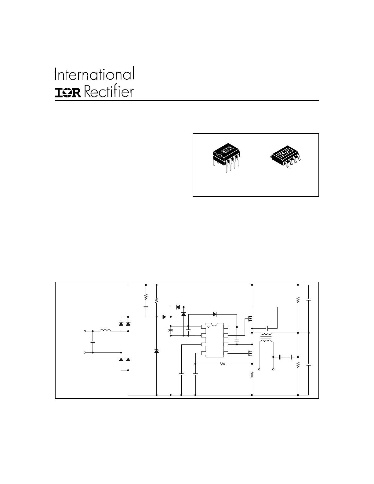
Description
The IR2161 is a dedicated Intelligent Half bridge Driver IC for a Halogen convertor (electronic transformer). It
includes all necessary protection features and also allows the Convertor to be dimmed externally with a
standard phase cut dimmer with both leading or trailing edge types. This IC provides the advantage of reduced
thermal stress in the lamp due to softstart. There is also compensation of the output voltage for load regulation.
It enables the convertor to operate with extremely low harmonic distortion over the full range of loads. The
IR2161 includes adaptive deadtime to allow cool running MOSFETs and improves the EMI behaviour due to
frequency modulation (dither). All the features are integrated in a small 8 pin DIP/SOIC package to allow for a
size reduction in the next generation of convertors.
Typical Connections
AC LINE
INPUT
CLF
LF
D1 D2
D3 D4
RD
CD
RS
DCP1
CS
1
2
3
4
CCS
DB
8
IR2161
7
6
5
RL
Q1
Q2
OUTPUT
CSNUB
12VAC
VB
HO
CB
VS
LO
RCS
CVCC2
DCP2
VCC
COM
CSD
CSD
DS
CVCC1
VZ
R1
T1
C3 C4
R2 C2
C1
Note: Throughout this data sheet “convertor” is spelled in accordance with standard IEC 61047 “DC or AC supplied convertors
for filament lamps – Performance requirements”.
www.irf.com 1
Page 2
IR2161(S) & (PbF)
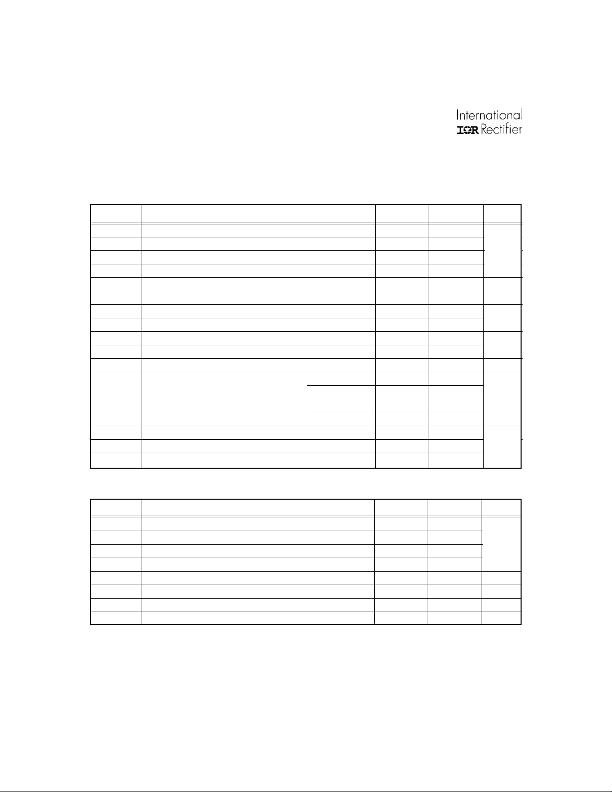
Absolute Maximum Ratings
Absolute maximum ratings indicate sustained limits beyond which damage to the device may occur. All voltage parameters
are absolute voltages referenced to COM, all currents are defined positive into any lead. The thermal resistance and power
dissipation ratings are measured under board mounted and still air conditions.
Symbol Definition Min. Max. Units
V
B
V
S
V
HO
V
LO
IO
MAX
V
CSDMAX
V
CS
I
CS
I
CC
dV/dt Allowable offset voltage slew rate -50 50 V/ns
P
D
Rth
JA
T
J
T
S
T
L
High side floating supply voltage -0.3 625
High side floating supply offset voltage VB - 25 VB + 0.3
High side floating output voltage VS - 0.3 V
B
+ 0.3
Low side output voltage -0.3 VCC + 0.3
Maximum allowable output current (HO,LO) due to external -500 500
power transistor miller effect
CSD pin voltage -0.3 V
Current sense pin voltage -0.3 V
CC
CC
+ 0.3
+ 0.3
Current sense pin current -5 5
Supply current (Note 1) -20 20
Maximum power dissipation @ T
PD = (T
JMAX-TA
)/Rth
(8 Lead SOIC) — 0.625
JA
≤ +25°C (8 Lead DIP) — 1
A
Thermal resistance, junction to ambient (8 Lead DIP) — 125
(8 Lead SOIC) — 200
Junction temperature -55 150
Storage temperature -55 150
Lead temperature (soldering, 10 seconds) — 300
V
mA
V
mA
W
°C/W
°C
Recommended Operating Conditions
For proper operation the device should be used within the recommended conditions.
Symbol Definition Min. Max. Units
V
BS
V
BSMIN
V
S
V
CC
I
CC
C
SD
I
CS
T
J
Note 1: This IC contains a zener clamp structure between the chip VCC and COM which has a nominal breakdown
Note 2: Enough current should be supplied into the VCC pin to keep the internal 15.6V zener clamp diode on this pin
2 www.irf.com
High side floating supply voltage VCC - 0.7 V
CLAMP
Minimum required VBS voltage for proper HO functionality 4.3 —
Steady state high-side floating supply offset voltage -1 600
Supply voltage V
CCUV+
V
CLAMP
V
Supply current (Note 2) 10 mA
CSD pin external capacitor 47 — nF
Current sense pin current -1 1 mA
Junction temperature -25 125 °C
voltage of 15.6V. Please note that this supply pin should not be driven by a DC, low impedance power source
greater than the V
regulating its voltage, V
specified in the Electrical Characteristics section.
CLAMP
.
CLAMP
Page 3
IR2161(S) & (PbF)
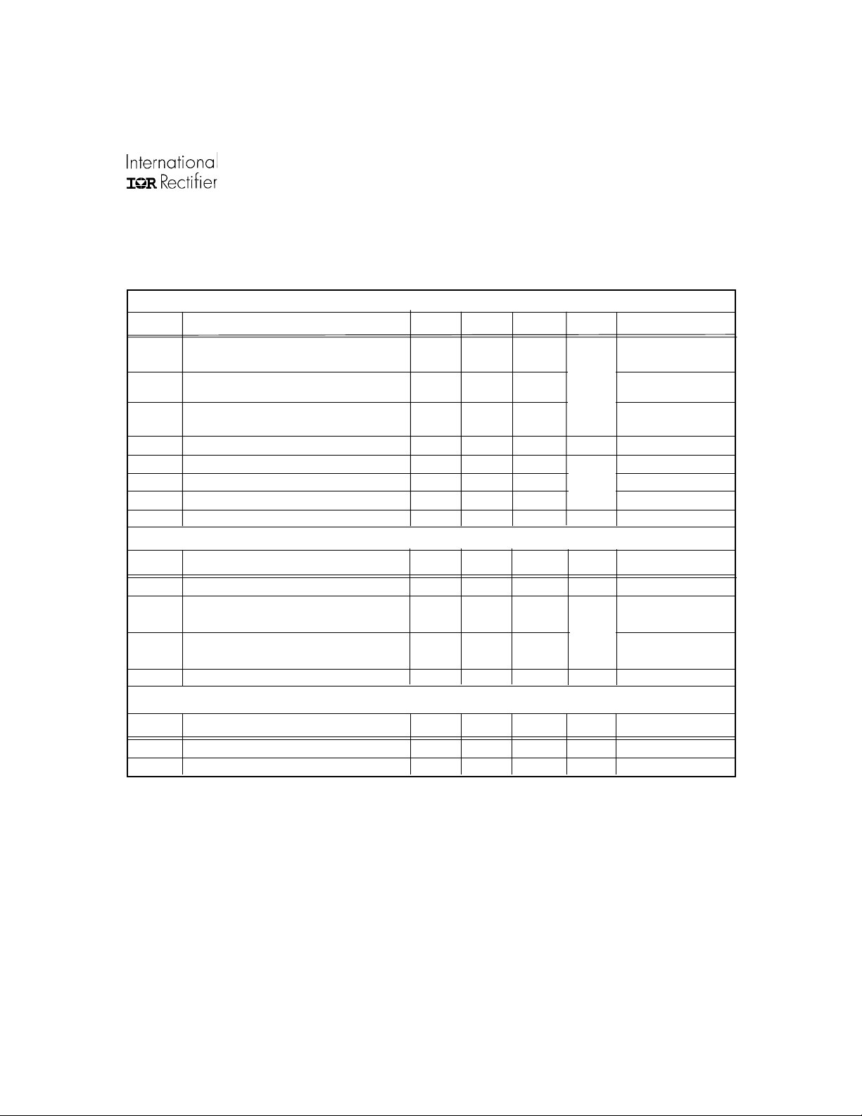
Electrical Characteristics
VCC = VBS = V
Supply Characteristics
Symbol Definition Min. Typ. Max. Units Test Conditions
V
CCUV+VCC
V
CCUV-
V
CCUVL-VCC
I
QCCUV
I
CCFLT
I
VCC current (low frequency) — 2.0 3.0 VCC=14V,VCSD=5.2V
CC
LF
I
VCC current (high frequency) — 4.0 7.0 VCC=14V,VCSD=0V
CC
HF
V
CLAMPVCC
Floating Supply Characteristics
Symbol Definition Min. Typ. Max. Units Test Conditions
V
BSM IN
I
BSHF
I
BSLF VBS
I
LEAK
= 14V, +/- 0.25V, VCSD = 5.0V, C
BIAS
supply undervoltage positive going
threshold 11.5 12.1 12.7 VCC rising from 0V
VCC supply undervoltage negative going
threshold 10 10.5 11 VCC falling from 14V
supply softstart reset negative going
threshold — — 5.5 VCC - V
UVLO mode quiescent current — 250 300 VCC = 11V
Fault-mode quiescent current — 1.4 2.0 CS=8V, VCSD=0V
zener clamp voltage 14.5 15.4 16.5 V ICC = 5mA
Minimum V
V
high frequency supply current — 3.0 — VCC=14V,VBS=14V,
BS
low frequency supply current — 0.8 — VCC=14V,VBS=14V,
Offset supply leakage current — — 50 µAV
to start oscillation at HO 3.0 3.6 4.3 V
BS
LO =CHO
= 1000 pF, and TA = 25°C unless otherwise specified.
V
(-2V)
µA
mA
mA
CCUV-
VCSD=0V
VCSD=5.2V
= VS = 600V
B
Voltage Compensation Characteristics (Run Mode)
Symbol Definition Min. Typ. Max. Units Test Conditions
V
CSD (min)
V
CSD (max)
www.irf.com 3
Min CSD voltage (in Run Mode) — 0 — V VCS = 0V
Max CSD voltage (in Run Mode) — 5.5 — V VCS = 0.4V
Page 4
IR2161(S) & (PbF)
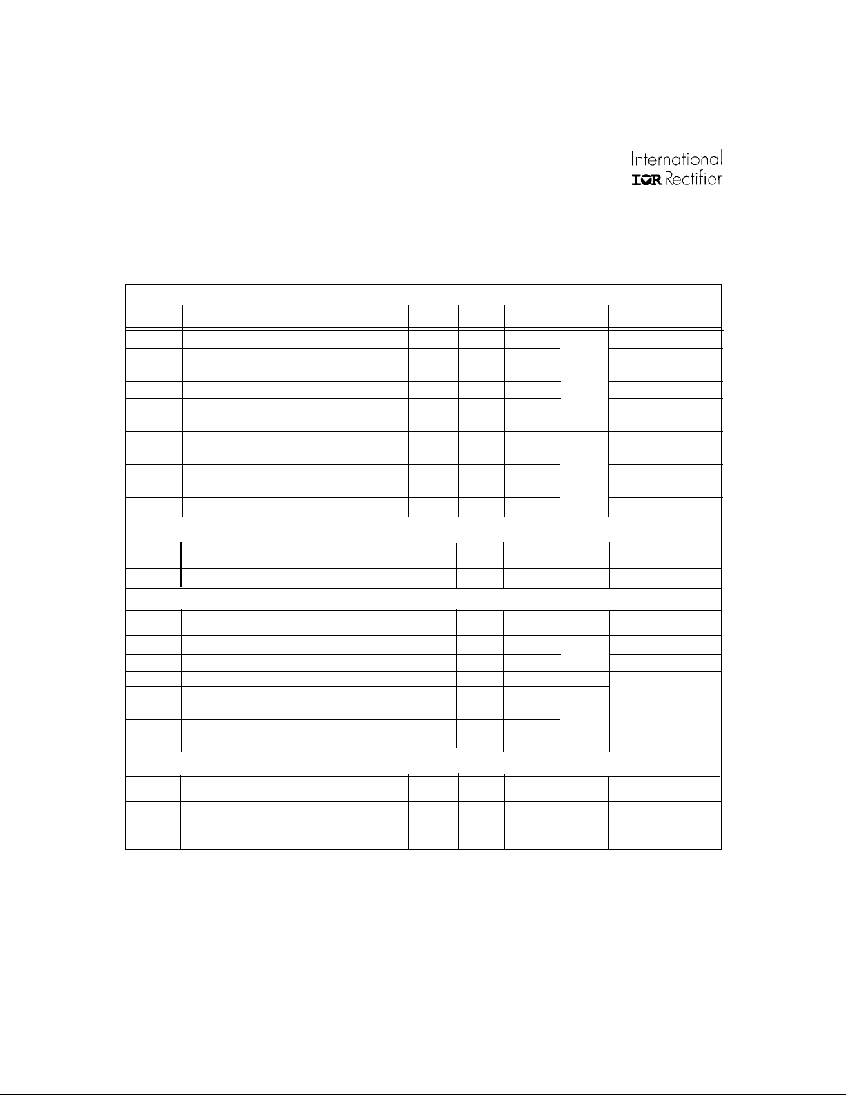
Electrical Characteristics (cont’d)
VCC = VBS = V
Shutdown Circuit Characteristics
Symbol Definition Min. Typ. Max. Units Test Conditions
V
CSOL
V
CSSC
I
OL
I
SC
I
RESET
V
CSLATCH
T
CSLATCH
V
CSDOL
V
CSDSD
V
CSDRS
Thermal Shutdown Characteristics
Symbol Definition Min. Typ. Max. Units Test Conditions
T
SD
Oscillator Characteristics
= 14V, +/- 0.25V, VCSD = 5.0V, C
BIAS
Overload threshold (CS PID) 0.47 0.56 0.64
CSD short circuit threshold (CS PID) 1 1.2 1.4
CSD overload charging current
CSD short circuit charging current 75 100 120 VCS=1.5V,VCSD=7V
CSD shutdown reset current 0.1 0.7
Latched shutdown threshold
Latched shutdown delay 1 µsec VCS>VCSLATCH
Begin fault timing
Positive going threshold for oscillator
shutdown
Negative going threshold for oscillator restart
Latched over temperature limit
LO =CHO
= 1000 pF, and TA = 25°C unless otherwise specified.
V
6
—
—
—
—
—
9 12 VCS=0.8V,VCSD=7V
uA
9
5
12
2.4
135
—
—
—
—
—
—
oC
VCSD=14V
V
VCS>VCSOL
VCS > VCSOL
V
Symbol Definition Min. Typ. Max. Units Test Conditions
f
(min)
f
(max)
D Oscillator duty cycle
LO(max)
DT
DT
HO(max)
Minimum oscillator frequency — 34 — VCSD = 5.3V
Maximum oscillator frequency in RUN mode
Maximum LO output deadtime — 1.0 —
(run mode default)
Maximum HO output deadtime — 1.0 —
(run mode default)
—
70
— 50 — %
—
kHz
µsec
VCSD = 0V
no reset from ADT
Adaptive Dead-Time System Characteristics
Symbol Definition Min. Typ. Max. Units Test Conditions
DT
DT
LO(min)
HO(min)
Minimum LO output deadtime — 700 —
Minimum HO output deadtime — 700
—
4 www.irf.com
Minimum propagation
nsec
delay from ADT to
output drivers
Page 5
IR2161(S) & (PbF)
Electrical Characteristics (cont.)
VCC = VBS = V
Soft Start Characteristics
Symbol Definition Min. Typ. Max. Units Test Conditions
I
SS
f
SS
Gate Driver Output Characteristics
Symbol Definition Min. Typ. Max. Units Test Conditions
V
V
V
V
t
RISE
t
FALL
IO+ HO, LO source current — 200 —
IO- HO, LO sink current — 300 —
LO voltage when LO is low — COM —
LO=LOW
HO=LOW
LO voltage when LO is high — VCC —
LO=HIGH
HO voltage when HO is high — VCC —
HO=HIGH
Turn-off fall time — 60 140
= 14V, +/- 0.25V, VCSD = 5.0V, C
BIAS
Soft start CSD charge current — 0.5 — mA
Soft start frequency
HO voltage when HO is low — COM —
Turn-on rise time — 110 250
LO =CHO
= 1000 pF, and TA = 25°C unless otherwise specified.
—
115
—
kHz VCC>VCCUV+
CHO=CLO=1nFns
mA
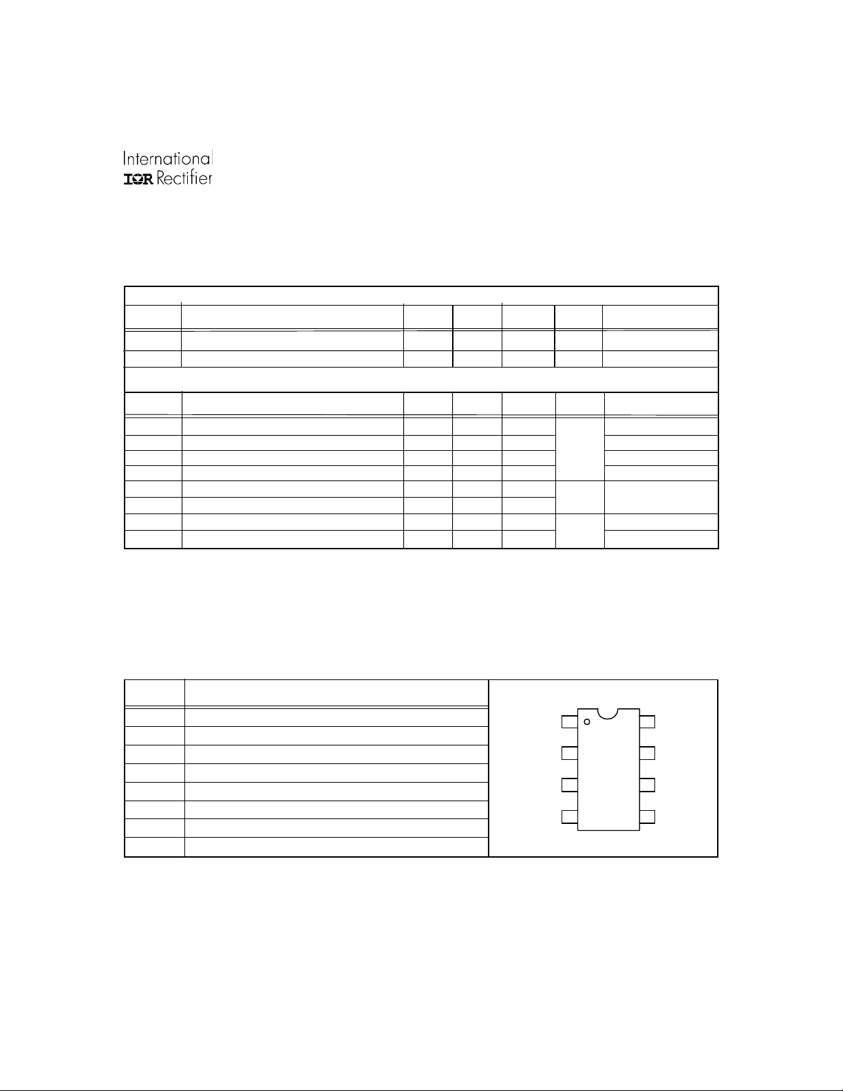
Lead Definitions
Lead Assignments
Symbol Description
V
CC
COM IC power and signal ground
CSD Shutdown timing and compensation capacitor
CS Current sensing input
LO Low-side gate driver output
V
S
HO High side gate driver output
V
B
* Recommended value for CSD is 100nF (all performance data relates to this value)
NOTE: The recommended value for RL is 1K Ohm and CCS is 1nF.
www.irf.com 5
Supply voltage
High-side floating return
High side gate driver floating supply
VCC
COM
CSD
CS
1
IR2161
2
3
4
8
VB
HO
7
6
VS
5
LO
Page 6
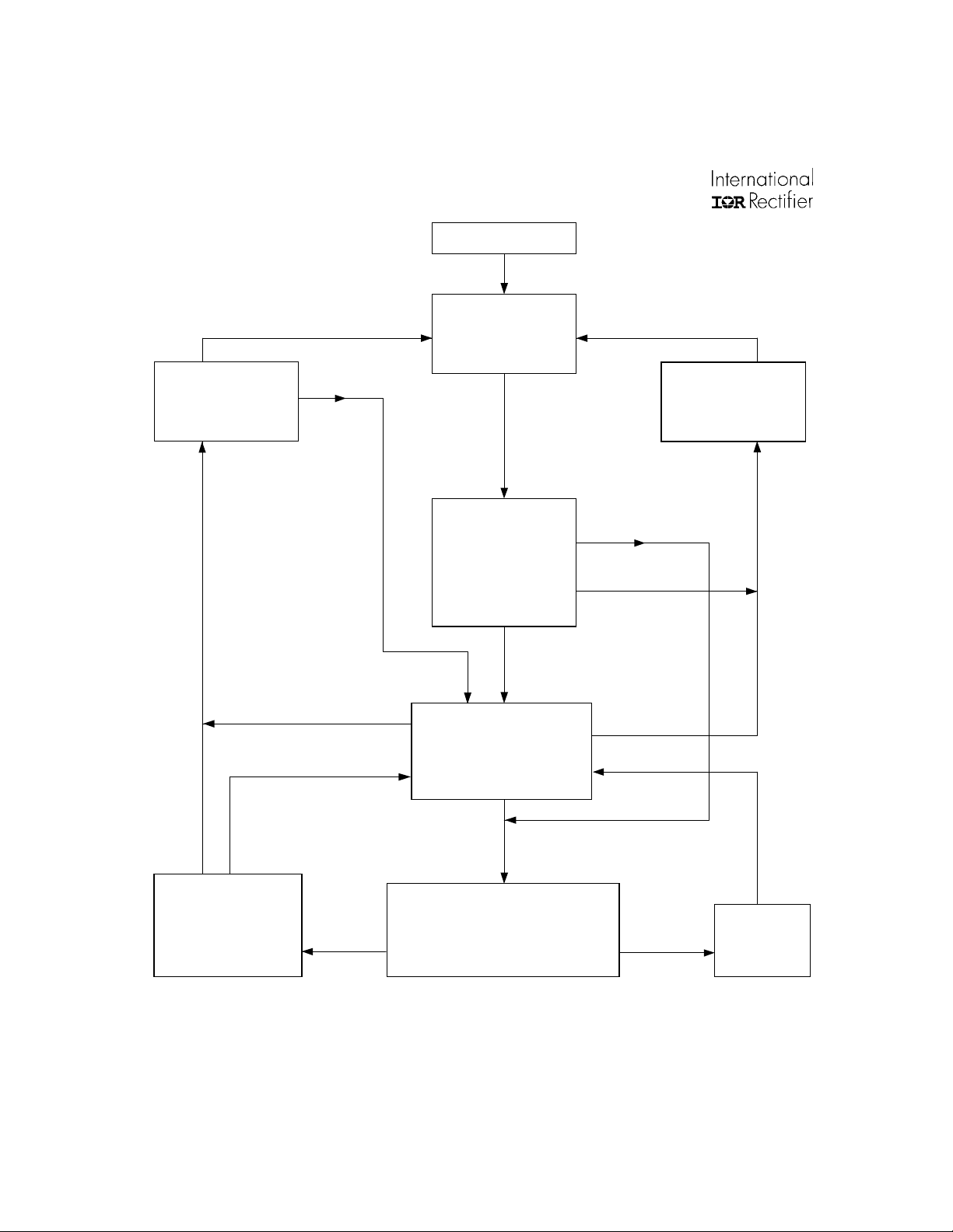
IR2161(S) & (PbF)
Power Turned On
VCC < 5.5V (V
(Power Turned Off)
STANDBY Mode
1
/
-Bridge Off
2
≅
I
QCC
Oscillator Off
µ
A
300
VCC < 10.5V (V )
(Phase Cut Dimming)
VCC < 10.5V (V )
(Phase Cut Dimming)
Auto-Restart Timeout
(V
< 2.4V) (V
CSD
CSD switched to run mode
CCUVL-
VCC > 12.1V(V
T
<135 C
J
Oscillator On
CCUV-
CCUV-
)
CSDRS
)
CCUV+
jmax
)
)
o
(T
UVLO Mode
1
-Bridge Off
/
2
≅
I
QCC
Oscillator Off
CSD = 0V
300
A
µ
VCC > 12.1V
T
<135 C
J
o
(V
CCUV+
(T
)
jmax
VCC < 5.5V (V
(Power Turned Off)
)
CCUVL-
)
FAULT Mode
1
/
-Bridge Off
2
Oscillator Off
Oscillator On
SOFTSTART
Mode
1
/
- Bridge On
2
Initial frequency 130kHz
CSD charged from Isource
Fault Detected
CS
(Vpk at V
T
<135 C
J
> 0.56V)(V )
o
(T
)
jmax
(Over-Temperature)
CSOL
Frequency ramps down to
f(min)
CSD
V
> 5.2V
(End of SOFTSTART Mode)
CSD switched to Comp function
Fault Detected
CS
(V
<135 C
J
CSLATCH
o
> 9V)
)
(T
jmax
)
RUN Mode
Voltage compensation active
CSD varies between
VCSD (min)
to V
CSD(max)
= 0 for f
= 5.5V for f
(min)
(Vpk at V
T
(Over-Temperature)
CSD switched to
run mode
(max)
SHUTDOWN Mode
1
/
-Bridge Off
2
CSD is slowly discharged
Fault Confirmed
> 12V)
CSD
(V
(V
)
CSDSD
Fault Timing Mode
1
/
CSD initialized to 5V (V
VCS >0.56V(V
V
> 1.2V (V
CS
CSOL
CSSC
Fault Detected (Vpk at VCS > 0.56V (V ))
CSD switched to Shutdown Circuit
CSD discharged to 0V
Frequency defaults to f(min)
- Bridge On
2
CSDOL
)
)=Overload:CSD slow charge
Fault Removed
(Vpk at VCS < 0.5V)
(V )
) = Short Circuit : CSD
fast charge
CSOL
CSOL
Delay
CSD is slowly
discharged to 2.4V
CSDRS
(V
)
All values are typical
NOTE: If the IR2161 die temperature exceeds 135o at any time the system will enter FAULT Mode. At a typical frequency of
40kHz, the die temperature is approximately 12oC above the ambient air temperature
6 www.irf.com
Page 7

Block Diagram
IR2161(S) & (PbF)
0.54V
www.irf.com 7
Page 8

IR2161(S) & (PbF)
Halogen Convertor Controller
Functional Description
Under-voltage Lock-Out Mode (UVLO)
The under-voltage lockout mode (UVLO) is defined as the
state the IC is in when VCC is below the turn-on threshold.
To identify the different modes of operation, refer to the
State Diagram shown on page 7 of this data sheet. The
IR2161 under voltage lock-out is designed to maintain an
ultra low supply current of less than 300uA, and to guarantee the IC is fully functional before the high and low side
output drivers are activated. Figure 1 shows a simple VCC
supply arrangement that will work effectively, also when
the convertor is being dimmed from a conventional triac
based wall dimmer
RD
RS
CD
BR
LF
CF
The start-up capacitor (C
supply resistor (RS) minus the start-up current drawn by
the IC. This resistor is chosen to provide sufficient current
to supply the IR2161 from the DC bus. In a Halogen convertor it is important to consider that the DC bus is completely
unsmoothed and has a full wave rectified shape. C
be large enough to hold the voltage at Vcc above the UVLO
threshold for one half cycle of the line voltage as it will only
be charged at the peak. A charge pump consisting of two
diodes (DCP1 and DCP2) connected to CSNUB is recommended to supply VCC as this allows RS to be a large value
since it is only needed at startup. IF RS is required to supply
the circuit without a charge pump it needs to be a relatively
low value and consequently dissipates 1 to 2W, which is
undesirable.
An external 16V zener diode DZ has been added to avoid
the need for the internal zener to dissipate power (it should
DS
CVCC
DZ
DB
VCC
1
IR2161
COM
2
CSD
3
CS
4
CSD
CCS
M1
VB
8
HO
7
CB
VS
6
LO
M2
5
RL
RCS
Figure 1, Halogen Convertor.
) is charged by current through
VCC
OUTPUT
VCC
should
be rated at 1.3W). The resistor RD in series with CD is
necessary if the convertor is required to operate from a
triac based (leading edge) phase cut dimmer. When the
triac fires at a point during the mains half-cycle the high dv/
dt allows a large current to flow through this path to instantly
charge C
to the maximum Vcc voltage.
VCC
The external zener (DZ) will prevent possible damage to
the IC by shunting excess current to COM.
Once the capacitor voltage on VCC reaches the start-up
threshold the IC turns on and HO and LO begin to
oscillate.
The supply resistor (RS) and RD/CD must be selected such
that enough supply current is available over all ballast
operating conditions. A bootstrap diode (DB) and supply
capacitor (CB) comprise the supply voltage for the high
side driver circuitry. To guarantee that the high-side supply
is charged up before the first pulse on pin HO, the first
pulse from the output drivers comes from the LO pin. During
under voltage lock-out mode, the high and low-side driver
outputs HO and LO are both low.
Soft Start Mode
The soft start mode is defined as the state the IC is in at
system switch on when the lamp filament is cold. As with
any type of filament lamp, the Dichroic Halogen lamp has a
positive temperature coefficient of resistance such that the
cold resistance (at switch on when the lamp has been off
long enough to cool) is much lower than the hot resistance
when the lamp is running. This normally results in a high
inrush current occurring at switch on. Under worst-case
conditions this could potentially trigger the convertor’s shut
down circuit. To overcome this problem the IR2161
incorporates the soft start function.
When the IC starts oscillating the frequency is initially very
high (about 130kHz). This causes the output voltage of the
convertor to be lower since the HF transformer in the system
has a fixed primary leakage inductance that will present a
higher impedance at higher frequency and thus allowing
less AC voltage to appear across the primary. The reduced
output voltage will naturally result in a reduced current in
the lamp which eases the inrush current thus avoiding
tripping of the shutdown circuit and will ease the stress on
the lamp filament as well as reducing the current in the half
bridge MOSFETs (M1 and M2).
The frequency sweeps down gradually from 130kHz to the
8 www.irf.com
Page 9

IR2161(S) & (PbF)
minimum frequency over a period of around 1s (assuming
CSD=100nF). During this time the external capacitor at the
CSD pin charges from 0V to 5V, controlling the oscillator
frequency through the internal voltage controlled oscillator
(VCO). The value of CSD will determine the duration of the
soft start sweep. However, since it also governs the shut
down circuit delays, the value should be kept at 100nF to
achieve the datasheet operation.
ISS
CSD
5V
Figure 2, Halogen Convertor.
It can be seen from Figure 2, that at switch on, the CSD
capacitor is internally switched to the soft start circuit input.
A current source charges CSD linearly to 5V over a period
of 0.5s at which time the comparator output goes high. The
PMOS switch opens and the ISS current source is
disconnected from CSD. The comparator latches high at this
point and this causes the oscillator range to change and the
CSD capacitor to be disconnected from the soft start circuit
and connected to the voltage compensation circuit. The
latching comparator has a built in delay of at least 20uS in
order to prevent false triggering caused by transients.
Set Oscillator
Range
Figure 4, Cold Lamp Inrush Current with Soft Start.
Run Mode (Voltage Compensation)
When soft start is completed the system switches over to
compensation mode. This function provides some regulation of the output voltage of the convertor from minimum to
maximum load. In this type of system it is desirable that the
voltage supplied to the lamp does not exceed a particular
limit. If the lamp voltage becomes too high the temperature
of the filament runs too high and the life of the lamp is
significantly reduced. The problem is that the output transformer is never perfectly coupled so there will always be a
degree of load regulation.
The transformer has to be designed such that the lamp
voltage at maximum load is sufficiently high to ensure
adequate light output.
At minimum load the voltage will consequently be higher
and is likely to exceed the maximum desired lamp voltage.
In the widely used self-oscillating system based around
bipolar power transistors, there is some frequency change
(increasing the frequency reduces the output voltage)
depending on the load that helps to compensate for this,
although this is non-linear and depends on many parameters
in the circuit and so is not easy to predict.
The IR2161 based system includes a function that monitors
the load current through the current sense resistor (RCS).
Figure 3, Typical Cold Lamp Inrush Current.
The peak current is detected and amplified within the IC
then appears at the CSD pin during run mode. The voltage
www.irf.com 9
Page 10

IR2161(S) & (PbF)
across the CSD capacitor will vary from 0V if there is no
load to approximately 5V at maximum load.
This is provided that the correct value of current sense
resistor has been selected for the maximum rated load and
line voltage supply of the convertor. This should be 0.33
Ohm (0.5W) for a 100W system running from a 220-240V
AC line. (It should be noted that the RCS resistor value is
also critical for setting the limits for the shut down circuit)
In RUN mode the oscillator frequency will vary from
approximately 34kHz when VCSD is 5V (maximum load) to
70kHz when VCSD is 0V (no load). The result of this is that
if a lighter load, such as a single 35W lamp, is connected to
a 100W convertor, the frequency will shift upwards so that
the output voltage falls below the maximum that is desirable
for the lamp. This provides sufficient compensation for the
load to ensure that the lamp voltage will always be within
acceptable limits but does not require a complicated regulation
scheme involving feedback from the output.
An additional internal current source has been included to
discharge the external capacitor. This will provide
approximately 10% ripple at twice the line frequency if CSD
is 100nF.
The advantage of this is that during the line voltage half
cycle the oscillator frequency will vary by several kHz thus
spreading the EMI conducted and radiated emissions over
a range of frequencies and avoiding high amplitude peaks
at particular frequencies. In this way the filter components
used may be similar to those used in a common bipolar self-
Figure 6, VS voltage and CSD voltage.
In the above trace it can be seen that a leading edge phase
cut (triac) dimmer is connected at close to maximum
brightness. There is a short delay at the beginning of each
half cycle before the AC line voltage is switched to the
convertor. Dimming increases the ripple in the CSD voltage
and gives more modulation. This is an inherent effect that
causes no system problems.
The startup sequence of the CSD pin can be seen from the
point where VCC increases above the UVLO+ threshold.
AV > 13
CS
12K
oscillating system.
Figure 5, Voltage Compensation Circuit
150K
CSD
Figure 7, Startup sequence of CSD.
This trace shows that after the CSD voltage has ramped up
through soft start, the system switches over to voltage compensation mode and a ripple exists which allows the frequency modulation (or “dither”) to occur. In this case the
10 www.irf.com
Page 11

IR2161(S) & (PbF)
convertor is close to maximum load. If the load is reduced,
the average level at which the ripple occurs (i.e. the DC
component) will be at a lower level.
Shut Down Circuit
The IR2161 contains a dual mode auto-resetting shutdown
circuit that detects both a short circuit or overload condition
in the convertor. The load current detected at the CS pin is
used to sense these conditions. If the output of the convertor
is short-circuited, a very high current will flow in the half
bridge and the system must shut down within a few mains
half cycles, otherwise the MOSFETs will rapidly be destroyed
due to excessive junction temperature. The internal CS pin
has an internal threshold (V
threshold so that if the voltage exceeds this level for more
than 50mS, the system will shut down.
A delay is included to prevent false tripping either due to
lamp inrush current at switch on (this current is still higher
than normal with the soft start operation) or transient
currents that may occur if an external triac based phase
cut dimmer is being used.
There also exists a lower threshold (V
much longer delay before it shuts down the system. This
provides the overload protection if an excessive number of
lamps is connected to the output or the output is shortcircuited at the end of a length of cable that has sufficient
resistance to prevent the current from being large enough
to trip the short circuit protection. Also under this condition
there is an excessive current in the half bridge that is
sufficient to cause heating and eventual failure but over a
longer period of time. The threshold for overload shutdown
is approximately 50% above maximum load with a delay of
approximately 0.5s. These timings are based on a current
waveform that has a sinusoidal envelope and a high
frequency square wave component with 50% duty cycle.
Both shutdown modes are auto resetting, which allows the
oscillator to start again approximately 1.5s after shutting
down. This is so that if the fault condition is removed the
system can start operating normally again without the line
voltage having to be switched off and back on again. It also
provides a good indication of overload to the end user as all
the lamps connected to the system will flash on and off
continuously if too many are connected.
The shut down circuit also uses the external CSD capacitor for
it’s timing functions. When the 0.5V threshold (V
ceeded at CS the CSD is internally disconnected from the voltage
compensation circuit and connected to the shutdown circuit.
). There also exists a lower
CSSC
), which has a
CSOL
CSOL
) is ex-
1.2V
Shutdown Functi on
0.54V
Overload Functi on
I_SC
I_OL
12V
2.5V
4V
RQ
I_RESET
QS
Enable OutputsCS
Switch
CSD
Figure 8, Shut Down Circuit.
The oscillator operates at minimum frequency when the
CSD capacitor is required for shutdown circuit timing.
During soft start or run mode, if the 0.5V threshold (V
CSOL
is exceeded the IR2161 charges CSD rapidly to approximately 5V (V
CSDOL
).
When the voltage at the CS input is greater than 0.5V, the
CSD capacitor is charged by current source IOL and when
the short circuit threshold of 1.2V is exceeded it is charged
by ISC as well. If 1.2V is exceeded CSD will charge from 5V
(V
CSDOL
) to 12V (V
), in approximately 50ms. When
CSDSD
0.5V is exceeded but 1.2V is not, CSD charges from 5V
(V
CSDOL
) to 12V (V
) in approximately 0.5s. It should
CSDSD
be remembered that, the timing accounts for the fact that
high frequency pulses with approximately 50% duty cycle
and a sinusoidal envelope appear at the CS pin.
The values of ISC and IOL take into account that only at the
peak of the mains will the comparator outputs go high and
effectively the capacitor will be charged in steps each line
half cycle. Once VCSD reaches 12V (V
discharges down to 2.4V (V
) and the system starts
CSDRS
CSDSD
), VCSD
up again. If the fault mode is still present, CSD starts
charging again.
If a fault is detected but goes away before CSD reaches
12V (V
), then CSD will discharge to 2.4V (V
CSDSD
CSDRS
and then the system will revert to compensation mode
without interruption of the output.
Following a shutdown, when the system starts up again
after the delay, the CSD capacitor will be internally switched
back to the voltage compensation circuit. However, if the
fault is still present the system will switch CSD back to the
shutdown circuit again.
)
)
www.irf.com 11
Page 12

IR2161(S) & (PbF)
Figure 9, Short Circuit Output Current.
In addition, any time Vcs exceeds VCSLATCH
(approximately half Vcc), this latching shutdown function
will be triggered and the system will remain in FAULT mode
until VCC is re-cycled.
The IR2161 also includes over temperature shutdown, which
latches the convertor off when the die temperature of the
IC exceeds 130-135
that the die temperature will be no more than 20
the ambient temperature at all operating frequencies inside
the convertor.
°C. Experimental measurements reveal
°C above
Calculating Rcs
The value of the current sense resistor Rcs is critical to
achieve correct operation in the IR2161 based Halogen
convertor.
DC Bus
Voltage
VS
LOAD
1/2 DC Bus
Voltage
VCSpk
VCS
RCS
Figure 10, Overload Output Current.
In figures 9 and 10, trace (1) shows the half bridge
oscillations during both types of fault mode and trace (2)
shows the charging and discharging of the CSD capacitor.
The IR2161 can also be externally shut off by applying a
voltage above 9V (VCSLATCH) to the CS pin. This will
cause the system to go directly to a latched fault mode,
after a delay of approximately 1uS to avoid the possibility of
false tripping caused by transients. To restart the system, it
is necessary to cycle Vcc off and on.
Ignoring the output transformer we can assume for this
calculation that the load is connected from the half bridge to
the mid point of the two output capacitors and that the
voltage at this point will be half the DC bus voltage. The
RMS voltage of the DC bus is the same as that of the AC line
so we can see that the RMS voltage across the load shown
in Figure 8, will be half the RMS voltage of the line. The load
is the maximum rated load of the convertor. The current in
Rcs will be half the load current given by :
12 www.irf.com
Figure 11, Calculating RCS
Page 13

IR2161(S) & (PbF)
P
I =
RMSCS
Since the load is resistive the current waveform will have a
sinusoidal envelope and so the peak can be easily determined taking into account that the current has a high frequency component with an approximate 50% duty cycle:
Therefore:
For correct operation at maximum load the peak voltage
should be 0.4V.
The calculation can be simplified by combining the formulae,
=
R
CS
Which can be simplified to:
R ⋅= 141.0
CS
LOAD
)(
V
AC
22
II ×=
)()(
V
⋅
4.0
⋅⋅
22
V
P
CS
P
LOAD
AC
LOAD
)()(
RMSCSPKCS
RIV ×=
CSPKCSPKCS
In this case :
2
100
=×
W062.033.0
230
It is important to bear in mind that the resistor must be rated
to handle this current in a high ambient temperature.
IMPORTANT NOTE
The filter resistor RL should be 1K, which is needed to
protect the CS input from negative going transients. CCS
should be 1nF and is also necessary to filter out switching
transients that can impair the operation of the shutdown
circuit.
Adaptive Dead Time
Because of the fact that the DC bus voltage varies during
the mains half cycle, the dead time may need to vary in
order to achieve soft switching. The IR2161 has an adaptive dead time circuit (ADT) that detects the point at which
the voltage at the half bridge slews to 0V (COM) and sets
the LO output high at this point. There is an internal sample
and hold system that allows approximately the same delay
to be used to set HO high after LO has gone low. This
reacts on a cycle-by-cycle basis of the oscillator and therefore will adjust the dead time as necessary regardless of
external conditions.
Example
For a 100W convertor working from a 230VAC supply the
current sense resistor would need to be :
×
230141.0
324.0
Ω=
100
The nearest preferred value to this would be 0.33 Ohms.
The power dissipation in Rcs should also be considered
and is given by :
2
LOAD
V
AC
R
CS
Figure 12, ADT when VS slews from VBUS to COM
P
P ×
=
CS
www.irf.com 13
Page 14

IR2161(S) & (PbF)
Figure 12, ADT when VS slews from COM to VBUS
The above waveforms are typical, showing the operation
of the ADT circuit in either direction. In this case the design
could be optimized further by increasing the snubber capacitor to slightly increase the slew time, in order to account for the propagation delays in the system. Alternatively an output transformer with a greater leakage inductance can extend the period before the VS voltage turns
around and starts to go back the other way again.
The designer does not need to take into account parasitic
capacitances in the MOSFETs or leakage inductance in the
output transformer and fix the dead time accordingly.
The system can operate reliably down to dead times in the
order of 300nS, which should be low enough to
accommodate the output transformer leakage inductance
and parasitic MOSFET capacitances of a practical Halogen
convertor.
The slew rate can easily be increased, if necessary, by
adding a small snubber capacitor across the primary of the
transformer if necessary. However, should the snubber
capacitor be too large, it will prevent the VS voltage from
slewing all the way to the opposite rail. Consequently the
ADT function will be unable to operate, causing the IR2161
to revert to the default dead time of 1µS. Snubber capacitors
would normally be in the order of hundreds of pF.
of the power MOSFETs in the half-bridge will be at a
maximum. At lighter loads there may be hard switching if
the VS voltage is unable to slew all the way or it slews so
rapidly that the voltage begins to turn around again before
the IR2161 is able to switch on the relevant MOSFET in the
half bridge.
Such a situation is not desirable but may be acceptable at
lighter loads where the conduction losses are small.
With correct optimization of the output transformer and
surrounding circuit it is possible to achieve a design that
will not hard switch from 20% to 100% of the maximum
rated load of the system.
This system avoids the need for an external resistor to
program the dead time and contributes to the multi functional nature of the CSD pin to the IR2161 being realized
with only 8 external pins
In any design when there is no load at the output, the VS
voltage will not slew and obviously the ADT circuit is not
able to function in this condition. In this case the dead time
will default to approximately 1µS, the maximum allowed by
the IC and there will be hard switching.
Although this will inevitably lead to some switching losses,
there are no conduction losses so the temperature rise of
the half bridge MOSFETs should not create a problem in this
case.
Dimming
Almost any Halogen convertor available can be dimmed by
an external phase cut dimmer that operates in trailing edge
mode. This means that at the beginning of the line voltage
half cycle, the switch inside the dimmer is closed and mains
voltage is supplied to the convertor allowing the convertor
to operate normally. At some point during the half cycle, the
switch inside the dimmer is opened and voltage is no longer
applied. The DC bus inside the convertor almost immediately
drops to 0V and the output is no longer present. In this way
bursts of high frequency output voltage are applied to the
lamp. The RMS voltage across the lamp will naturally vary
depending on the phase angle at which the dimmer switch
switches off. In this way the lamp brightness may easily
be varied from zero to maximum output.
When designing a halogen convertor it is desirable to optimize
the system at maximum load, where the conduction losses
14 www.irf.com
Page 15

IR2161(S) & (PbF)
DC BUS VOLTAGE
LAMP VOLTAGE
Figure 13, Trailing Edge Dimming
Trailing edge dimmers are less common however than leading
edge dimmers. This is because they are more expensive to
make and need to incorporate a pair of MOSFETs or IGBTs
whereas a leading edge dimmer is based around a single
triac.
Conversely many Halogen convertors are not able to operate with leading edge dimmers because of the fact that
they are based around a triac. It is possible, however, to
design a Halogen convertor that will work effectively with
a triac based dimmer by designing the input filter components correctly ensuring that at the firing point of the triac
the oscillator can start up rapidly. In the IR2161 based system this is easy to achieve through the addition of RD and
CD, which conduct a large current to VCC due to the high
dv/dt that occurs when the triac fires. At the same time, the
bus voltage rises rapidly from zero to the AC line voltage. If
the VCC voltage falls below V
the triac in the dimmer is off, the soft start will not be initiated because the soft start circuit is not reset until VCC
drops approxmately 2V below V
time as the VCC capacitor discharges very slowly during
UVLO micro-power operation. The intermediate period is
referred to as Standby mode.
during the time when
CCUV-
. This takes some
CCUV-
DC BUS VOLTAGE
LAMP VOLTAGE
Figure 14, Leading Edge Dimming
holding current. If the load is purely resistive (as in a filament lamp directly connected to the dimmer) this will naturally happen at the end of the line voltage half cycle as the
current has to fall to zero. In a Halogen convertor it is necessary to place a capacitor and inductor at the AC input to
comply with regulations regarding EMI conducted emis-
sions. This means that when the line voltage falls to zero
there could still be some current flowing that is enough to
keep the triac switched on and so the next cycle will follow
through and not be phase cut as required. This can happen
intermittently resulting in flickering of the lamps. The way to
avoid the problem is to ensure that the product has the
smallest possible filter capacitor CCS and to state a minimum load for the convertor. This would be typically one
third of the maximum load to avoid problems of this kind.
During dimming the voltage compensation circuit will cause
a frequency shift upward at angles above 90° because the
peak voltage at CS will be reduced (see figure 14). This will
result in a reduction of voltage at CSD and thus an increase
in frequency. However this will not have a noticeable effect
on the light output.
The problem associated with operation of Halogen convertors with triac dimmers is due to the fact that after a triac
has been fired it will conduct until the current falls below its
Figure 15, Half Bridge voltage and current during dimming
www.irf.com 15
Page 16

IR2161(S) & (PbF)
5
5
)
a
5
15
VCCUV+
12
9
VCC(V)
6
3
0
-25 0 25 50 75 100 12
VCCUV-
Temperature (°C)
Graph : VCCUV +/- vs TEMP (IR2161)
20
VCCLAMP_25ma
15
VCCLAMP_5ma
5
4
3
2
IQCC (mA
1
0
-25 0 25 50 75 100 12
ICCHF
ICCLF
IQCCFLT
Temperature (°C)
Graph : IQCC vs TEMP (IR2161)
6
5
4
VCSDMAX
10
VCCLAMP_5_25m
5
3
VCSD (V)
2
1
VCSDMIN
0
-25 0 25 50 75 100 125
Temperature (°C)
Graph : VCCLAMP_5_25ma vs TEMP (IR2161)
0
-25 0 25 50 75 100 12
Temperature (°C)
VCSDMIN,MAX vs TEMP (IR2161)
16 www.irf.com
Page 17

IR2161(S) & (PbF)
5
5
5
5
2
1.5
VCS_SC
1
VCSOL, VCSSC (V)
0.5
VCS_OL
0
-25 0 25 50 75 100 12
Temperatur e (°C)
VCS_OL, VCS_SC vs TEMP (IR2161)
100
20
15
10
I (uA)
5
I_OL
I_RESET
0
-25 0 25 50 75 100 12
Temperature ( °C)
I_RESET, I_OL vs TEMP (IR2161)
12
VCSD_SD
VCSD_OL
I(uA)
90
80
70
I_SC
9
6
VCSD (V)
3
VCSD_RS
60
-25 0 25 50 75 100 12
Temperature (°C)
I_SC vs TEMP (IR2161)
0
-25 0 25 50 75 100 12
Temperature (°C)
Graph : VCSDSD,OL,RS vs TEMP (IR2161)
www.irf.com 17
Page 18

IR2161(S) & (PbF)
5
5
175
150
125
100
75
Frequency (kHz)
50
25
0
-25 0 25 50 75 100 12
FSS
FRUN
FMIN
Temperatur e (°C)
Frequency vs TEMP (IR2161)
1
0.8
0.6
Iss (uA)
0.4
0.2
0
-25 0 25 50 75 100 12
Temperature (°C)
Graph : Iss (uA) vs TEMP (IR2161)
18 www.irf.com
Page 19

Case outlines
IR2161 8-Lead PDIP
IR2161(S) & (PbF)
01-6014
01-3003 01
(MS-001AB)
A
E
D B
5
87
6
6X
0.25 [.010]
65
H
4312
0.25 [.010] A
e
8X b
e1
A1
A
CAB
NOTES:
1. DIMENS IO NING & TOLE RAN CING PE R ASME Y14.5M-1994.
2. CONTROLLING DIM ENSION: MILLIMETER
3. DIMENSIONS ARE SHOWN IN MILLIMETERS [INCHE S].
4. OUTLINE CONFORMS TO JEDEC OUTLINE MS-012AA.
IR2161S 8-Lead SOIC
C
0.10 [.004]
6.46 [.255]
3X 1.27 [.050]
y
DIM
FOOTPRINT
8X 0.72 [.028]
8X 1.78 [.070]
MIN MAX
.0532
A
.0040
A1
b
.013
c .0075 .0098 0.19 0.25
D
.189
E
.1497
.050 B ASIC
e
.025 BA SIC 0.635 BA SIC
e1
.2284
H
.0099
K
.016
L
y
0°
K x 45°
8X L
8X c
7
5 DIMENSION DOES NOT INCLUDE MOLD PROTRUSIONS.
MO LD P ROTR US IO NS N OT TO EX CE ED 0.15 [.006].
6 DIMENSION DOES NOT INCLUDE MOLD PROTRUSIONS.
MO LD P ROTR US IO NS N OT TO EX CE ED 0.25 [.010].
7 DIMENSION IS THE LENGTH OF LEAD FOR SOLDERING TO
A SU BSTR ATE .
01-0021 11
.0688
.0098
.020
.1968
.1574
.2440
.0196
.050
8°
MILLIMETERSIN C H E S
MIN MAX
1.35
1.75
0.10
0.25
0.33
0.51
4.80
5.00
3.80
4.00
1.27 BA SIC
5.80
6.20
0.25
0.50
0.40
1.27
0°
8°
01-6027
(MS-012AA)
www.irf.com 19
Page 20

IR2161(S) & (PbF)
LEADFREE PART MARKING INFORMATION
Part number
Date code
Pin 1
Identifier
?
MARKING CODE
Lead Free Released
P
Non-Lead Free
Released
IRxxxxxx
YWW?
ORDER INFORMATION
Basic Part (Non-Lead Free)
8-Lead PDIP IR2161 order IR2161
8-Lead SOIC IR2161S order IR2161S
IR logo
?XXXX
Lot Code
(Prod mode - 4 digit SPN code)
Assembly site code
Per SCOP 200-002
Leadfree Part
8-Lead PDIP IR2161 order IR2161PbF
8-Lead SOIC IR2161S order IR2161SPbF
IR WORLD HEADQUARTERS: 233 Kansas St., El Segundo, California 90245 Tel: (310) 252-7105
20 www.irf.com
This product has been qualified per industrial level MSL-3, Lead-free available
Data and specifications subject to change without notice. 9/19/2005
 Loading...