

Page 1
Preliminary Data Sheet No. PD60169-E
DIMMING BALLAST CONTROL IC
Features
Ballast control and half-bridge driver in one IC
•
T ransf ormer-less lamp power sensing
•
Closed-loop lamp power control
•
Closed-loop preheat current control
•
Programmable preheat time
•
Programmable preheat current
•
Programmable ignition-to-dim time
•
0.5 to 5VDC dimming control input
•
Min and max lamp power adjustments
•
Programmable minimum frequency
•
Internal current sense blanking
•
Full lamp fault protection
•
Description
Description: The IR2159/IR21591 are complete dimming ballast controllers and 600V
half-bridge drivers all in one IC. The architecture includes phase control for transformer-less lamp power sensing and regulation which minimizes changes needed to
adapt non-dimming ballasts for dimming. Externally programmable features such as
preheat time and current, ignition-to-dim time, and a complete dimming interface with
minimum and maximum settings provide a high degree of flexibility for the ballast
design engineer. Protection from failure of a lamp to strike , filament failures, thermal
overload, or lamp failure during normal operation, as well as an automatic restart
function, have been included in the design. The heart of this control IC is a voltagecontrolled oscillator with externally programmable minimum frequency. The IR2159/
IR21591 are available in both 16 pin DIP and 16 pin narrow body SOIC packages.
Brown-out protection
•
Automatic restart
•
Micro-power startup
•
Zener clamped V cc
•
Over-temperature protection
•
16-pin DIP and SOIC package types
•
Parameter IR2159 IR21591
Deadtime 1.8us 1.0us
Frequency
Range
IR2159
IR21591
See
Graph 3
Packages
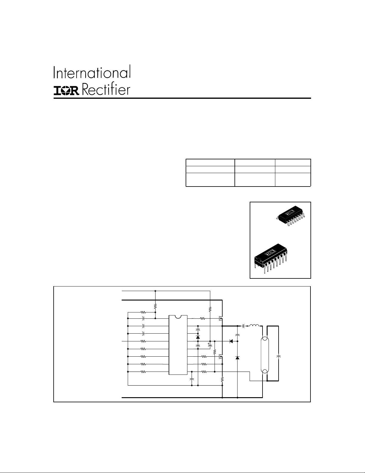
16 Lead SOIC
(narrow body)
(S)
(S)
See
Graph 4
16 Lead PDIP
T ypical Connection
+ Rectified AC Line
+ DC Bus
0.5 to 5VDC
- DC Bus
R
VAC
R
VDC
C
VDC
1
C
VCO
C
PH
R
DIM
R
MAX
R
MIN
R
FMIN
R
IPH
VDC
2
VCO
3
CPH
DIM
5
MAX
6
MIN
7
FMIN
8 9
IPH
R
PULL-UP
16
HO
15
VS
14
VB
134
VCC
12
COM
11
LO
10
CS
SD
R
CS
www.irf.com 1
Single Lamp Dimmable
Page 2
IR2159/IR21591
(S)
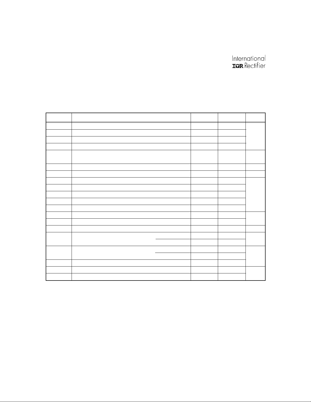
Absolute Maximum Ratings
Absolute maximum ratings indicate sustained limits beyond which damage to the device may occur. All voltage
parameters are absolute voltages referenced to COM, all currents are defined positive into any lead. The thermal
resistance and power dissipation ratings are measured under board mounted and still air conditions.
Symbol Definition Min. Max. Units
V
B
V
S
V
HO
V
LO
I
OMAX
V
VCO
I
CPH
V
IPH
V
DIM
V
MAX
V
MIN
V
CS
I
SD
I
CC
dV/dt Allowable offset voltage slew rate - 50 50 V/ns
P
D
Rth
JA
T
J
T
S
T
L
High side floating supply voltage -0.3 625
High side floating supply offset voltage VB - 25 VB + 25
High side floating output voltage VS - 0.3 V
B
+ 0.3
Low side output voltage -0.3 VCC + 0.3
Maximum allowable output current (either output) -500 500
due to external power transistor miller effect
mA
Voltage controlled oscillator input v oltage -0.3 6.0 V
CPH current -5 5 mA
IPH voltage -0.3 5.5
Dimming control pin input voltage -0.3 5.5
Maximum lamp power setting pin input voltage -0.3 5.5
V
Minimum lamp power setting pin input voltage -0.3 5.5
Current sense input voltage -0.3 5.5
Shutdown pin current -5 5
Supply current (note 1) — 25
Package power dissipation @ TA ≤ +25°C (16 pin DIP) — 1.60
P
D
(T
=
JMAX-TA
)/Rth
JA
(16 pin SOIC) — 1.25
Thermal resistance, junction to ambient (16 pin DIP) — 7 5
(16 pin SOIC) — 11 5
mA
W
o
C/W
Junction temperature -55 15 0
Storage temperature -55 15 0
o
Lead temperature (soldering, 10 seconds) — 300
V
C
Note 1: This IC contains a zener clamp structure between the chip VCC and COM which has a nominal breakdown
voltage of 15.6V (V
power source greater than the diode clamp voltage (V
). Please note that this supply pin should not be driven by a DC, low impedance
CLAMP
) as specified in the Electrical Characteristics
CLAMP
section.
2 www.irf.com
Page 3
IR2159/IR21591
(S)
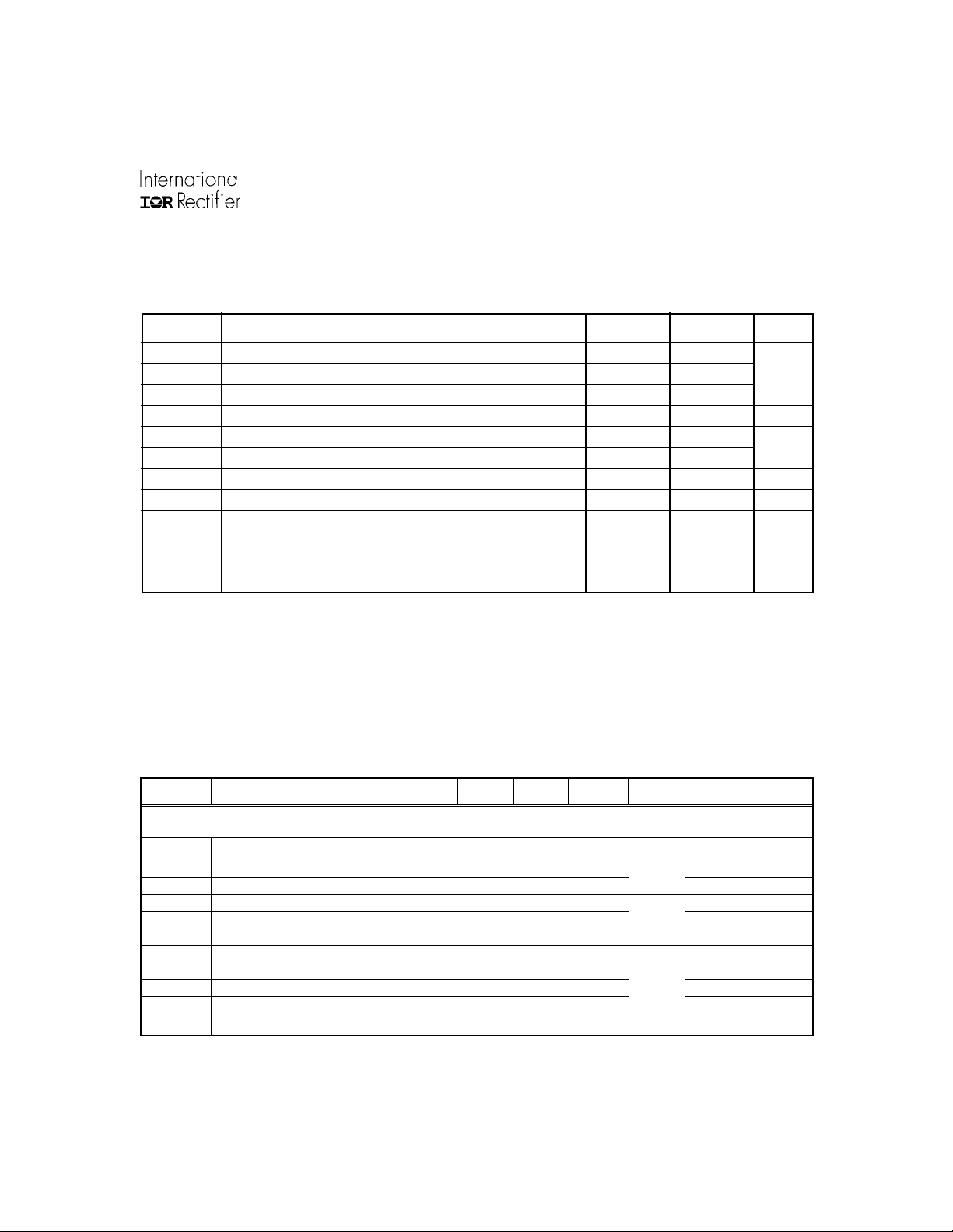
Recommended Operating Conditions
For proper operation the device should be used within the recommended conditions.
Symbol Definition Min. Max. Units
V
BS
V
S
V
CC
I
CC
V
VCO VCO pin voltage
V
DIM
V
MAX
V
MIN
R
FMIN
I
SD
I
CS
T
J
High side floating supply voltage VCC - 0.7 V
Steady state high side floating supply offset voltage -1 600
Supply voltage V
Supply current note 2 10 mA
DIM pin voltage 0 5
MAX pin current (note 3) -750 0
MIN pin voltage 1 3 V
Minimum frequency setting resistance 10 1 00
Shutdown pin current - 1 1
Current sensing pin current -1 1
Junction temperature -40 125
CCUV+VCLAMP (15.6)
05
CLAMP
V
V
µA
kΩ
mA
o
C
Note 2: Enough current should be supplied into the VCC lead to keep the internal 15.6V zener clamp diode on this lead
Note 3: The MAX lead is a voltage-controlled current source. For optimum dim interface current mirror performance,
regulating its voltage, V
this current should be kept between 0 and 750µA.
CLAMP
.
Electrical Characteristics
VCC = VBS = V
R
= 56k, V
MIN
Symbol Definition Min. Typ. Max. Units Test Conditions
Supply Characteristics
V
CCUV+ VCC
V
CCHYS VCC
I
QCCUV
I
QCCFLT
I
QCCFMIN VCC
I
QCCFMAX VCC
I
QCCFMIN VCC
I
QCCFMAX VCC
V
CLAMP VCC
= 14V +/- 0.25V, VCS = 0.5V, VSD = 0.0V, R
BIAS
= 0.0V, C
CPH
supply undervoltage positive going 12.0 12.5 13.0
threshold
supply undervoltage lockout hysteresis 1.5 1.6 1.7
UVLO mode quiescent current — 200 — VCC = 10V
Fault-mode quiescent current — 240 — SD=5V, CS=2V, or
supply current @ FMIN (IR2159) — 5.6 — V
supply current @ FMAX (IR2159) — 6.6 — V
supply current @ FMIN (IR21591) — 5.4 — V
supply current @ FMAX (IR21591) — 6.8 — V
zener shunt clamp voltage 14.5 15.6 16.5 V ICC = 10mA
= 1000pF, TA = 25oC unless otherwise specified.
LO,HO
FMIN
= 40k, C
VCO
= 10 nF, V
= 0.0V, R
DIM
V
µA
mA
MAX
Tj > TSD
VCO
VCO
VCO
VCO
= 33k,
= 0V
= 5V
= 0V
= 5V
www.irf.com 3
Page 4
IR2159/IR21591
(S)
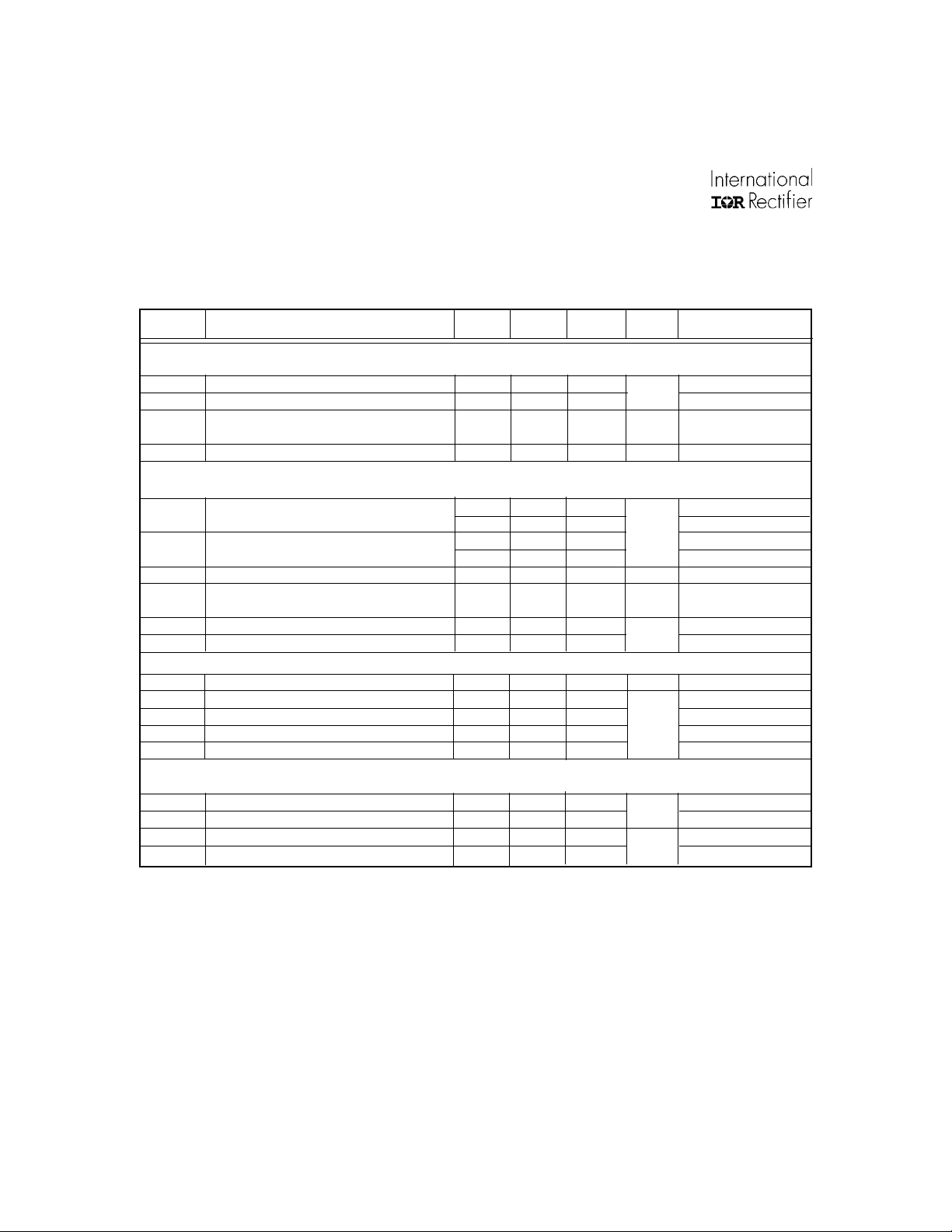
Electrical Characteristics (cont.)
VCC = VBS = V
R
= 56k, V
MIN
Symbol Definition Min. Typ. Max. Units Test Conditions
Floating Supply Characteristics
I
QBS0
I
QBS1
V
BSMIN
I
LK
Oscillator I/O Characteristics
f
vco
f
vco
d Gate drive outputs duty cycle
V
VCOFLT
IVCOPH Preheat mode VCO pin discharge current
IVCODIM Dim mode VCO pin discharge current
= 14V +/- 0.25V, VCS = 0.5V, VSD = 0.0V, R
BIAS
= 0.0V, C
TPH
Quiescent VBS supply current — 0 — VHO = V
Quiescent VBS supply current —
Minimum required VBS v oltage for proper
HO functionality
Offset supply leakage current — — 50
VCO frequency range (IR2159) — 25 —
(See graph 3) —
VCO frequency range (IR21591) — 30 —
(See graph 4) —
Fault-mode VCO pin voltage (UVLO,
shutdown, over-current/temp.)
= 1000pF, TA = 25oC unless otherwise specified.
LO,HO
= 40k, C
FMIN
— 4
—
—
—
1.0
—
VCO
30
95
230
50
5 V
16.0
= 10 nF, V
—V
5 V
—
—
—
—
—
= 0.0V, R
DIM
µA
µA
kHz
% V
µA
MAX
= V
HO
VB = VS = 600V
V
=0V, RFMIN=39KΩ
VCO
V
=5V, RFMIN=10KΩ
VCO
V
=0V, RFMIN=68KΩ
VCO
V
=5V, RFMIN=10KΩ
VCO
VCO
VCPH < 5V
= 33k,
S
B
= 0V
IVCOPK
t
DTLO
t
DTHO
t
DTLO
t
DTHO
Amplitude control VCO pin charging current — 60.0 —
LO output deadtime (IR2159)
HO output deadtime (IR2159)
LO output deadtime (IR21591)
HO output deadtime (IR21591)
— 1.8 —
— 1.8 —
— 1.0 —
— 1.0 —
µA
µs
V
CPH
< 5V, V
CS
Gate Driver Output Characteristics
VOL Low-level output voltage — — 100
VOH High-level output voltage — — 100 V
tr Turn-on rise time — — 150
tf T urn-off fall time
—
—
100
4 www.irf.com
mV
ns
BIAS
- Vo
>
V
IPH
Page 5
IR2159/IR21591
(S)
Electrical Characteristics (cont.)
VCC = VBS = V
R
= 56k, V
MIN
Symbol Definition Min. Typ. Max. Units Test Conditions
Preheat Characteristics
ICPH CPH pin charging current
VCPHIGN CPH pin ignition mode threshold voltage
VCPHCLMP CPH pin clamp voltage —
IIPH IPH pin DC source current — 25.0 — µAIIPH = 1/RFMIN
VCSTH Peak preheat current regulation threshold — 0.7 — V VCSTH =(IIPH) x (RIPH)
VCPHFLT CPH pin voltage during UVLO or fault —
Ignition Characteristics
V
CSTH
Protection Characteristics
V
SDTH+
V
VDCTH+
V
SDHYS
V
VDCHYS
V
SDCLMP
V
CSTH
T
SD
= 14V +/- 0.25V, VCS = 0.5V, VSD = 0.0V, R
BIAS
= 0.0V, C
TPH
Peak over current threshold — 1.6 — V VCPH < 5V
Rising shutdown pin threshold voltage — 2.0 —
Rising VDC pin threshold voltage — 5. 1 —
SD threshold hysteresis — 150 — mV
VDC threshold hysteresis — 2. 1 —
SD pin clamp voltage — 7. 6 — ISD = 100mA
Peak ov er-current latch threshold voltage — 1.6 —
Thermal shutdown junction temperature —
= 1000pF, TA = 25oC unless otherwise specified.
LO,HO
—
—
FMIN
= 40k, C
1.3
5.0
10
0.0
165 —
VCO
= 10 nF, V
—
—
—
—
= 0.0V, R
DIM
µA
V
V SD = 5V, or CS = 2V,
or Tj
V
V
o
C
V
MAX
CPH
= 33k,
> TSD
>
5.1V
Phase Control
V
CSTHZX
R
FB
t
Blank
Zero-crossing threshold voltage — 0.0 — V
Phase control FB resistor (Internal) — 5.7 — kΩ
Zero-crossing internal blank time — 400 — ns
Dimming Interface
V
DIMOFF
V
DIM
V
MINMIN
V
MINMAX
V
DIMTH
V
DIMTH DIM mode VCO Threshold (IR21591)
Minimum Frequency Setting
V
FMIN
V
FMINFLT
www.irf.com 5
DIM pin offset voltage — 0.5 —
DIM pin input voltage range 0.0 — 5.0
DIM minimum reference voltage (MIN pin) — 1.0 —
DIM maximum reference voltage (MIN pin) — 3.0 —
DIM mode VCO Threshold (IR2159) — 0.5 —
— 1.1 —
FMIN pin voltage during normal operation — 5.1 — V
FMIN pin voltage during fault mode — 0.0 — V
V
= 5V
DIM
V
V
= 0V
DIM
SD = 5V, or CS = 2V,
or Tj
> TSD
Page 6
IR2159/IR21591
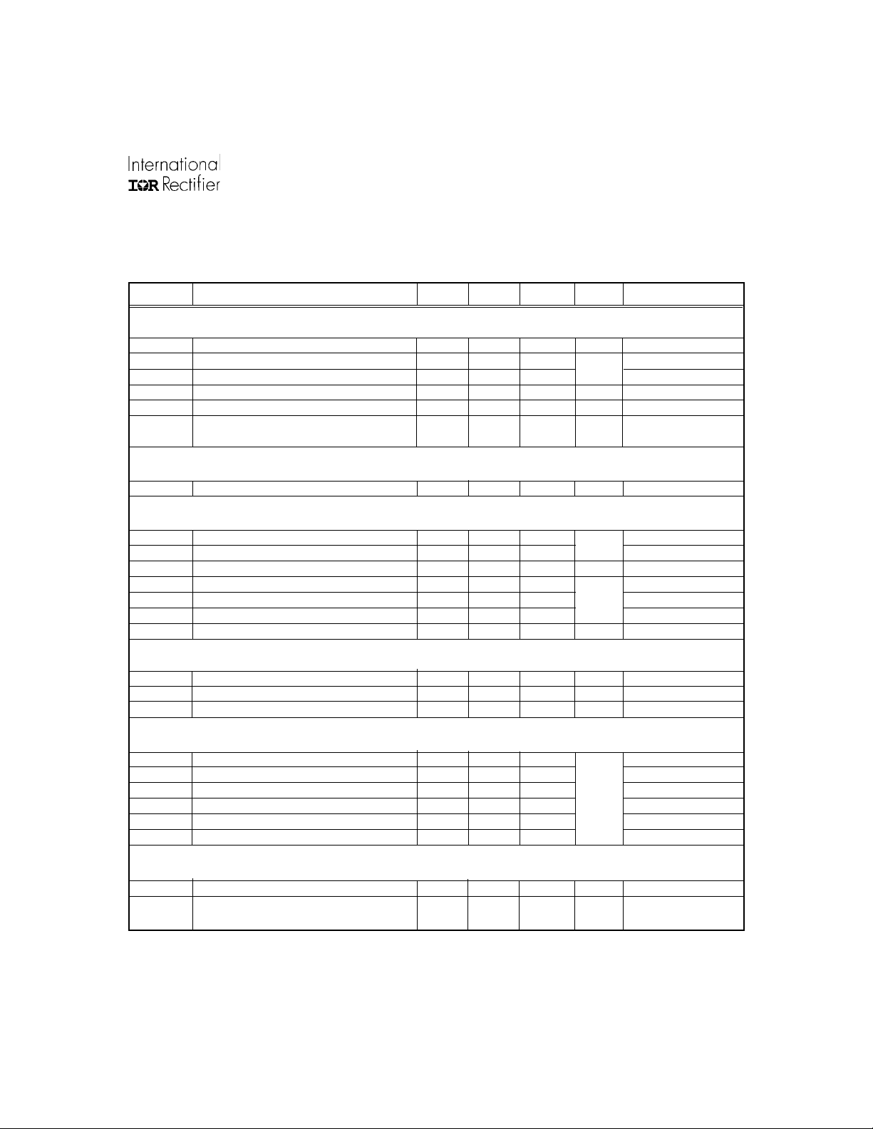
Block Diagram
(S)
5.1V
VCC
I
R
FB
15uA
1.3uA
RQ
I
DIM
4/R
FMIN
I
/5
DIM
1/R
1.6V
FMIN
CT
V
DIMTH
10 CYCLES
IGNITION
COUNTER
IDT+I
RQ
CT
I
CT
CT
QS
REF
QS
FB
3V
5.1V
1
0
VCO
VDC
CPH
DIM
MAX
MIN
FMIN
IPH
60uA
2
1uA
1
3
10V
4
5
6
I
FMIN
7
5.1V
8
Lead Assignments & Definitions
QS
RQ
5.1V
1.0V
CT
UNDER-
VOLTAGE
DETECT
14
VB
SHIFT
PULSE
FILTER &
LATCH
400ns
DELAY
15.6V
2.0V
7.6V
16
HO
15
VS
13
VCC
11
LO
12
COM
10
CS
9
SD
LEVEL
ERR
T
R1
R2 Q
QS
QS
Q
RQ
RQ
OVER-
TEMP
DETECT
Pin Assignments
1
VDC
2
VCO
3
CPH
4
DIM
5
MAX
6
MIN
7
FMIN
8
IPH
16
HO
15
VS
14
VB
13
VCC
12
COM
11
LO
10
CS
9
SD
Pin # Symbol Description
Line input voltage detection
Voltage controlled oscillator Input
Preheat timing input
0.5 to 5VDC dimming control input
Maximum lamp power setting
Minimum lamp power setting
Minimum frequency setting
Shutdown input
Current sensing input
Low-side gate driver output
IC power & signal ground
Logic & low-side gate driver supply
High-side gate driver floating supply
High voltage floating return
High-side gate driver output
15
10
11
12
13
14
16
1
2
3
4
5
6
7
8
9
VDC
VCO
CPH
DIM
MAX
MIN
FMIN
IPH Peak preheat current reference
SD
CS
LO
COM
VCC
VB
VS
HO
6 www.irf.com
Page 7
State Diagram
(
g)
(
)
Power Turned On
UVLO Mode
1/2-Bridge Off
IQCC=200mA
CPH=0V
Oscillator Off
IR2159/IR21591
(S)
SD > 2.0V
(Lamp Removal)
or
VCC < 10.9V
(Power Turned Off)
FAULT Mode
Fault Latch Set
1/2-Bridge Off
I
=240µA
QCC
CPH=0V
VCC=15.6V
Oscillator Off
CS > V
CSTH
(Over-Current or Hard Switching)
or
TJ > 165C
(Over-Temperature)
TJ > 165C
(Over-Temperature)
CS > V
CSTH
Failure to Strike Lamp
or Hard Switchin
or
TJ> 165C
Over-Temperature
(1.6V)
(1.6V)
PREHEAT Mode
1/2-BridgeOscillator On
V
(Peak Current Control)
CSPK+VIPH
CPH Charging@I
DIM+Open Circuit
Over-Current Disabled
IGNITION Mode
fPH ramps to fMIN
CPH Charging@I
DIM=Open Circuit
Over-Current Enabled
DIM Mode
PhaseCS=Phase
DIM=CPH
Over-Current Enabled
and
and
and
+1µA
+1µA
REF
DIMTH
(UV+)
(Bus OK)
(Lamp OK)
(T
jmax
VCC > 12.5V
VDC > 5.1V
SD < 1.7V
TJ < 165C
PH
CPH > 5.1V
(End of PREHEAT Mode)
PH
VCO < V
(End of IGNITION Mode)
VCC < 10.9V
(VCC Fault or Power Down)
or
VDC < 3.0V
(dc Bus/ac Line Fault or Power Down)
or
SD > 2.0V
)
(Lamp Fault or Lamp Removal)
www.irf.com 7
Page 8
IR2159/IR21591
(S)
Timing Diagram
Non-strike fault condition with lamp exchange
VCC
15.6V
UVLO+
UVLO-
VDC
VDCTH+
VDCTH-
CPH
5.1V
V
DIM
VCO
SD
HO
LO
CS
1.6V
V
5V
5V
IPH
PH FLT
IGN
SD PH
IGN
DIM UVLOUVLO
f
8 www.irf.com
Page 9

IR2159/IR21591
y
g
g
)
Q
g
g
g
ϕ
(Eq
)
y
ϕ
ϕ
y
)
)
(S)
External Components Selection Procedure
(Note:
Please refer to
"T
pical Connection"
dia
ram, page 1)
Set R
and R
VAC
on pin VDC will exceed 5.1 volts at the
desired line turn-on volta
The minimun operating frequency must
be lower than f
lower
. R
FMIN
, so R
I
IPH
FMIN
RCS sets the maximum ignition current
which corresponds to the maximum
i
nition voltage across the lamp.
The voltage at pin IPH is the reference
for amplitude current control durin
preheat mode. R
R
.
FMIN
such that the voltage
VDC
e.
of f
100%
also programs I
(whichever is
IGN
must be set first.
must be set after
IPH
MIN
and
R
Use Graph 5 or Graph 6
BEGIN
Calculate R
R
−
Calculate R
=
VDC
1
Select R
Calculate R
UPPULL
−
R
=
VAC
VAC
CS
VAC
=
I
1.5
1.5
I
IGN
PULL-UP
CCUV
VDC
−
ONTURN
−
ONTURN
FMIN
CS
6.1
PK
−
Select & Calculate R
Use Graph 8 to find I
then calculate R
=
R
IPH
IPH
RI
⋅
CSPH
PK
I
IPH
ONTURN
R
VAC
IPH
:
IPH
,
R
VDC
R
FMIN
R
CS
R
IPH
VAC
f
MIN
I
IGN
I
PH
TURN-ON
V
IGN
V
PH
During preheat, an internal 1.3 µA
current source at pin CPH char
es
external capacitor CCPH. Preheat mode
ends when VCPH exceeds 5.1 volts.
R
sets the lower phase boundar
MIN
corresponding to minimum lamp
power when V
be set after R
R
sets the upper phase boundar
MAX
corresponding to maximum lamp power
when V
after R
FMIN
DIM
FMIN
= 5 volts. R
DIM
and R
= 0 volts. R
.
must be set
MAX
.
MIN
MIN
must
Calculate
Calculate C
()
Calculate R
Find I
Find V
(Graph 7
MIN
uations 8 & 9
MIN
(Graph 9
MIN
V
R
=
MIN
I
Calculate R
Use Equation 15
MIN
MIN
CPH
teC
−=
76.2
PHCPH
MIN
MAX
C
CPH
R
MIN
R
MAX
t
PH
MINPLAMP
MAXPLAMP
www.irf.com 9
Page 10

IR2159/IR21591
Characteristic Curves
125
(S)
230
105
RFMIN=10K
85
RFMIN=16K
65
Frequency (KHz)
45
25
125
105
IN=20K
RFM
RFMIN=27K
RFMIN=39K
012345
(V)
V
VCO
85
Graph 1. F requency vs V
V
VCO
=5V
VCO
(IR2159)
190
RFMIN=10K
150
RFMIN=16K
110
70
RFMIN=20K
RFMIN=27K
RFMIN=39K
RFMIN=68K
Frequency (KHz)
30
012345
Graph 2. F requency vs V
(IR21591)
VCO
230
190
V
=5V
VCO
150
65
Frequency (KHz)
45
25
10 14 18 22 26 30 34 38
Graph 3. Frequency vs R
R
V
VCO
V
VCO
FMIN
=0.5V
=0V
K
Ω
FMIN
(IR2159)
110
Frequency (KHz)
V
VCO
=1.1V
70
V
=0V
VCO
30
10 20 30 40 50 60 70
R
K
Ω
FMIN
Graph 4. Frequency vs R
FMIN
(IR21591)
10 www.irf.com
Page 11

IR2159/IR21591
(S)
90
85
80
75
70
65
60
V
55
Frequency (KHz)
50
VCO
=0.5V
45
40
35
10 14 18 22 26 30 34 38
R
K
Ω
FMIN
Graph 5. Frequency vs R
450
400
350
300
( A)
250
MIN
I
200
150
100
50
10 20 30 40 50 60 70
R
FMIN
(KΩ)
FMIN
(IR2159)
170
160
150
140
130
120
V
=1.1V
110
Frequency (KHz)
VCO
100
90
80
10 14 18 22 26 30 34 38
K
R
Ω
FMIN
Graph 6. Frequency vs R
110
100
90
80
70
60
( A)
IPH
I
50
40
30
20
10
10 20 30 40 50 60 70
R
FMIN
(KΩ)
(IR21591)
FMIN
Graph 7. I
MIN
vs R
(IR2159/IR21591) Graph 8. I
FMIN
IPH
vs R
(IR2159/IR21591)
FMIN
www.irf.com 11
Page 12

IR2159/IR21591
(S)
0
-15
-30
I
VS
I/V
-45
VS
II
-60
-75
-90
1 1.25 1.5 1.75 2 2.25 2.5 2.75 3
V
(V)
MIN
Graph 9. ϕ IIVS/VVSI vs V
(IR2159/IR21591)
MIN
3
2.5
30
25
20
(KΩ)
MIN
R
15
10
5
2 2.2 2.4 2.6 2.8 3
(V)
V
MIN
Graph 10. R
MIN
vs V
MIN
150
140
RFMIN=39K
RFMIN=33K
RFMIN=27K
RFMIN=20K
RFMIN=16K
RFMIN=10K
2
A
µ
1.5
CPH
I
1
0.5
0
-25 0 25 50 75 100 125
Temperature °C
Graph 11. I
vs Temperature (IR2159/IR21591) Gr aph 12. I
CPH
130
A
µ
120
MIN
I
110
100
90
-25 0 25 50 75 100 125
Temperature °C
vs T emper ature (IR2159/IR21591)
MIN
12 www.irf.com
Page 13

IR2159/IR21591
(S)
40
36
32
(µA)
IPH
I
28
24
20
-25 0 25 50 75 100 125
Temperature °C
Graph 13. I
55
50
45
40
Frequency (KHz)
35
30
25
vs T emper ature (IR2159/IR21591) Graph 14. V
IPH
IR21591
IR2159
-25 0 25 50 75 100 125
Temperature °C
6
5.6
5.2
(V)
FMIN
V
4.8
4.4
4
-25 0 25 50 75 100 125
Temperature °C
vs Temperature (IR2159/IR21591)
FMIN
110
105
100
IR21591
95
90
85
80
75
Frequency (KHz)
70
65
60
IR2159
55
-25 0 25 50 75 100 125
Temperature °C
Graph 15. F requency vs Temperature
V
= 0V (IR2159/IR21591)
VCO
Graph 16. F requency vs Temperature
V
= 2V (IR2159/IR21591)
VCO
www.irf.com 13
Page 14

IR2159/IR21591
3
2.5
(S)
2
1.5
Dead Time Sec
1
0.5
0
-25 0 25 50 75 100 125
Temperature °C
Graph 17. Dead Time vs T emperature
(IR2159/IR21591)
IR2159
IR21591
14 www.irf.com
Page 15

IR2159/IR21591
%
%
%
%
g
(S)
Functional Description
Phase Control
To understand phase control, a simplified model
for the ballast output stage is used (Figure 1). The
lamp and filaments are replaced with resistors,
with the lamp inserted between the filament
resistors (R1, R2, R3 and R4).
R1 R2
L
Vin
Figure 1, Dimming ballast output stage.
During preheat and ignition (Figure 2), the circuit
is a high-Q series LC with a strong input current to
input voltage phase inversion from +90 to -90
degrees at the resonance frequency . For operating
frequencies slightly above resonance and higher ,
the phase is fixed at -90 degrees for the duration
of preheat and ignition. During dimming, the circuit
is an L in series with a parallel R and C, with a
weak phase inversion at high lamp power and a
strong phase inversion at lo w lamp power.
Rlamp
C
R3 R4
20
10
0
Magnitude [dB]
-10
-20
-30
5 101520253035404550
50%
100
Frequency [kHz]
PH/IGN
10%
50
100
PH/IGN
10
400
350
300
250
200
150
100
50
0
-50
-100
Phase [deg]
Figure 2, Typical output stage transfer function for
different lamp power levels.
In the time domain (Figure 3), the input current is
shifted -90 degrees from the input half-bridge
voltage during preheat and ignition, and
somewhere between 0 and -90 degrees after
ignition during running. Zero phase-shift
corresponds to maximum power
V
in
I
in
run
0
n
run
n
ph/ign
in
I
n
ph/i
t
Figure 3, Typical ballast output stage waveforms.
When the phase is calculated and plotted versus
lamp power (Figure 4), the result is a linear dimming
curve, even down to ultra-low light levels where
the resistance of the lamp can change by orders
of magnitude.
www.irf.com 15
Page 16

IR2159/IR21591
(S)
-60.0
-65.0
-70.0
-75.0
Phase [degrees]
-80.0
-85.0
-90.0
0 5 10 15 20 25 30
Lamp Po wer [Watts]
Figure 4, Lamp power vs. phase of output stage.
Under-voltage Lock-Out (UVLO)
The IR2159 undervoltage lock-out is designed to
maintain an ultra low quiescent current of less
than 200uA, while guaranteeing the IC is fully
functional before the high and low side output
drivers are activated. Figure 5 shows an efficient
supply voltage using the start-up current of the
IR2159 together with a charge pump from the
ballast output stage (R1, C1, C2, D1 and D2).
(+)
V
BUS
Rectified
AC Line
R3
VDC
1
CVDC
V
(-)
BUS
RVDC
16
15
14
13
12
11
VCC
COM
R1
HO
VS
C3
VB
D3
C1
LO
Q1
D1
Q2
RCS
Figure 5, Typical application of start-up circuitry.
Half-Bridge
Output
C2
D2
The start-up capacitor (C1) is charged by current
through resistor (R1) minus the start-up current
drawn by the IC . This resistor is typically chosen
to provide 2X the maximum start-up current at
low line to guarantee start-up under the worst case
condition. Once the capacitor voltage reaches the
start-up threshold, and, the voltage on pin VDC is
above 5.1V (see Brown-out Protection), the IC
turns on and HO and LO begin to oscillate. The
capacitor begins to discharge due to the increase
in IC operating current (Figure 6).
V
C1
V
UVLO+
VHYST
V
UVLO-
R1 & C1 TIME
CONSTANT
C1
DISCHARGE
INTERNAL
CLAMP VOLTAGE
DISCHARGE
TIME
CHARGE PUMP
OUTPUT
t
Figure 6, Start-up capacitor (C1) voltage.
During the discharge cycle, the rectified current
from the charge pump charges the capacitor above
the minimum operating voltage of the device and
the charge pump and internal 15.6V zener clamp
of the IC take over as the supply voltage. The
start-up capacitor and snubber capacitor must be
selected such that worst case IC conditions are
satisfied. A bootstrap diode (D3) and supply
capacitor (C3) comprise the supply voltage for
the high side driver circuitry. To guarantee that
the high-side supply is charged up before the first
pulse on pin HO, the first pulse from the output
drivers comes from the LO pin. During UVLO,
the high and low side driver outputs are low, pin
VCO is pulled-up internally to 5V resetting the
starting frequency to the maximum, and pin CPH
is short-circuited internally to COM resetting the
preheat time.
16 www.irf.com
Page 17

IR2159/IR21591
g
g
(S)
Brown-out Protection
In addition to the voltage on VCC being above
the start-up threshold, pin VDC must also be
above 5.1V for HO and LO to begin oscillating. A
voltage divider (R3,R VDC) from the rectified AC
line connected to pin VDC measures the rectified
AC line input voltage to the ballast and programs
the turn-on and turn-off line voltages. A filter
capacitor (CVDC) is also connected to pin VDC
that must be chosen such that the ripple is low
enough and the lower turn-off threshold of 3V is
not crossed during normal line conditions. This
detection is necessary due to the possibility of
the lamp extinguishing during low-line conditions
before the IC is properly reset. Should a brownout occur, the DC bus can drop to a level below
the minimum required for the tank circuit to
maintain the necessary lamp voltage. This
detection will insure a clean turn-off before the
DC bus drops too low and properly resets the
IC to the preheat mode when the line returns.
Preheat (PH)
The IR2159 enters preheat mode when VCC
exceeds the UVLO+ threshold and VDC exceeds
5.1V. HO and LO begin to oscillate at the
maximum operating frequency with 50% duty
cycle and at the internally set dead-time of 2us.
Pin CPH is disconnected from COM and an
internal 1uA current source (Figure 7) charges
the external timing capacitor on CPH linearly .
V
(+)
BUS
60uA
VCO
2
C
VCO
C
CPH
R
R
(-)
V
BUS
1uA
1uA
CPH
3
I
FMIN
FMIN
7
5.1V
FMIN
1/R
FMIN
IPH
8
IPH
VCO
Half
Brid
Driver
PH
LOGIC
7.6V
e
IR2159
HO
16
15
11
10
12
VS
LO
CS
COM
Q2
Q2
RCS
Half
Brid
Output
I
LOAD
Load
Return
e
Figure 7, IR2159 preheat circuitry.
An internal 1uA current source slowly discharges
the external capacitor on pin VCO and the voltage
on pin VCO begins to decrease . This decreases
the frequency, which, for operating frequencies
above resonance, increases the load current.
When the peak voltage measured on pin CS,
produced by a portion of the load current flowing
through an external sense resistor (RCS), exceeds
the voltage level on pin IPH, a 60uA internal
current source is connected to pin VCO and the
capacitor charges (Figure 8). This forces the
frequency to increase and the load current to
decrease. When the voltage on pin CS decreases
below IPH, the 60uA current source is
disconnected and the frequency decreases again.
www.irf.com 17
Page 18

IR2159/IR21591
(S)
HO
LO
VS
t
t
t
t
V
V
I
CVCO
60uA
CVCO
RCS
V
-1uA
IPH
Figure 8, Peak load current regulation timing diagram.
This feedback keeps the peak preheat current
regulated to the user-programmable setting on pin
IPH for the duration of the preheat time. An
internal current source connected to an external
resistor on pin IPH sets a voltage reference for
the peak pre-heat current. The pre-heat time
continues until the voltage on pin CPH exceeds
5V.
Ignition (IGN)
The IR2159 enters ignition mode when the voltage
on pin CPH exceeds 5V. The peak current
regulation reference voltage is disconnected from
the user-programmable setting on pin IPH and is
connected to a higher internal threshold of 1.6V
(Figure 9).
V
(+)
BUS
1.6V
IR2159
HO
VS
LO
CS
COM
Q2
Q2
RCS
Half
Bridge
Output
I
LOAD
Load
Return
16
15
11
10
12
0.5 to 5V
V
BUS
VCO
2
C
VCO
1uA
1uA
CPH
3
C
CPH
DIM
4
R
DIM
(-)
VCO
Half
Bridge
Driver
PH
LOGIC
7.6V
DIM
INTERFACE
FAULT
LOGIC
PHASE
CONTROL
Figure 9, IR2159 ignition circuitry.
The ignition ramp is then initiated as the capacitor
on pin VCO discharges linearly through an internal
1uA current source. The frequency decreases
linearly towards the resonance frequency of the
high-Q ballast output stage, causing the lamp
voltage and load current to increase (Figure 10).
The frequency continues to decrease until the lamp
ignites or the current limit of the IR2159 is reached.
If the current limit is reached, the IR2159 enters
FAULT mode. The 1.6V threshold together with
the external current sensing resistor on pin CS
determine the maximum allowable peak ignition
current (and therefore peak ignition voltage) of the
ballast output stage. The peak ignition current
must not exceed the maximum allowable current
ratings of the output stage MOSFETs or IGBTs,
and, the resonant inductor must not saturate
at any time.
Should the lamp ignite, the frequency continues
to decrease until the voltage on pin VCO reaches
VDIMTH, corresponding to the minimum operating
frequency set by the external resistor on pin FMIN,
18 www.irf.com
Page 19

IR2159/IR21591
g
g
(S)
and the IR2159 enters DIM mode and the phase
control loop is closed.
V
CPH
5.1V
R
& C
DIM
TPH
TIME CONSTANT
V
DIM
V
VCO
PH
IGN
IGN-TO-DIM
TIME
DIM
t
t
Figure 10, IR2159 ignition timing diagram.
For a reliable ignition with minimal start-up flash,
the resistor on FMIN should be set to 5kHz lower
than the ignition frequency or the 100% brightness
dimming frequency , whichev er is lower .
down smoothly to the user setting. Should the
ignition-to-dim time be too fast, how ever , the loop
can respond faster than the ionization constant
of the lamp (milliseconds) causing the VCO to
over-shoot. This can result in a frequency that is
higher than the minimum brightness frequency and
can extinguish the lamp. The capacitor on pin
CPH serves multiple functions by setting the
preheat time, the travel rate just after ignition
(together with resistor RDIM), and, serving as a
filter capacitor on pin DIM during dimming to
increase high-frequency noise immunity and
minimize component count.
Dimming (DIM)
To regulate lamp power, the error between the
reference phase and the phase of the output stage
current forces the VCO to steer the frequency in
the proper direction, as determined by the transfer
function of the output stage, such that the error is
forced to zero . An internal 15uA current source is
connected to pin VCO during dimming mode
(Figure 11) to discharge the VCO capacitor and
decrease the frequency towards lock.
V
(+)
Ignition-to-Dim (IGN-to-DIM)
When the VCO decreases below VDIMTH, the
IR2159 enters dim mode. The phase control loop
is closed and the phase of the load current is
regulated against the user control input on pin DIM.
To control the rate at which the dim setting
changes from maximum brightness to the user
setting (IGN-TO-DIM time , Figure 10), pin DIM is
connected internally to pin CPH when the IR2159
enters DIM mode. The resistor on pin DIM (RDIM)
discharges the capacitor on pin CPH down to the
user dim setting. The resistor can be selected for
a fast time constant to minimize the amount of
BUS
0.5 to 5V
V
BUS
VCC
R
FB
VCO
2
16uA
C
VCO
CPH
3
C
R
R
R
(-)
7.6V
CPH
DIM
4
DIM
MAX
5
MAX
MIN
6
MIN
PHASE
CONTROL
VCO
DIM
INTERFACE
IR2159
HO
16
Half
15
Brid
e
Driver
11
FAULT
LOGIC
1.6V
CS
10
COM
12
Q2
Half
Brid
Q2
RCS
Output
I
LOAD
Load
Return
e
VS
LO
flash visible ov er the lamp just after ignition, or, a
long time constant such that the brightness ramps
Figure 11, IR2159 dimming circuitry.
www.irf.com 19
Page 20

IR2159/IR21591
(S)
Once lock is achieved, the phase detector (PDET)
outputs short pulses to an open-drain PMOS that
charges the VCO capacitor through an inter nal
resistor (RFB) each time an error pulse occurs
(Figure 12). This action "nudges" the integr ator at
the input of the VCO to keep the phase of the
output stage current exactly locked in phase with
the reference.
V
CS
t
LO
n
REF
n
FB
n
ERR
V
VCO
t
Figure 12, Phase control timing diagram.
V
MIN
5V
V
R
MIN
3V
1V
0
0.5V 5V
R
MAX
SETTING
V
DIM
Figure 13, Dimming interface
USER
CT
LO
n
REF
0 -90 -180
---
DIM
RANGE
n
The charging time of CT from 1V to 5.1V
determines the on-time of output gate drivers HO
and LO and corresponds to -180 degrees of
possible phase shift in load current (minus
deadtime). For the 0 to -90 degree dim range, the
voltage on pin MIN is bounded between 1V and
3V using pins MIN and MAX. An external resistor
on pin MAX programs the minimum phase shift
reference (maximum lamp power) corresponding
to 5V on pin DIM, and an external resistor on pin
MIN sets the maximum phase shift (minimum
lamp power) corresponding to 0.5V on pin DIM.
The IR2159 includes a dimming interface for
analog lamp power control. The DIM pin input
requires a voltage in the range of 0.5 to 5VDC,
with 5V corresponding to minimum phase shift
(maximum lamp power). The output of the dim
interface is the voltage on pin MIN, which is
compared with the internal timing capacitor (CT)
voltage to produce a frequency-independent digital
reference phase (Figure 13).
Current Sensing
During dimming, the current sensing circuitry
(Figure 14) detects over-current which can occur
during hard-switching (see Fault section), and
zero-crossing to measure the phase of the total
load current. To reject any s witching noise which
can occur at the turn-on of the low-side MOSFET
or IGBT, a digital current sense blanking circuit
blanks out the signal from the zero-crossing
20 www.irf.com
Page 21

detection comparator for 400ns after LO goes 'high'
g
(+)
(-)
g
(Figure 15).
V
BUS
IR2159
IR2159/IR21591
V
CS
Switching
Noise
(S)
t
HO
16
Half
Brid
Driver
FAULT
LOGIC
PHASE
400ns
CONTROL
BLANK
V
BUS
VS
15
e
LO
11
1.6V
CS
10
COM
12
Q2
Half
e
Brid
Output
I
LOAD
Q2
R1
RCS
Load
Return
Figure 14, Current sensing circuitry.
The internal blank time reduces the dimming range
slightly (Figure 15) when operating at minimum
phase shift (maximum lamp power). The e xternal
programming resistor on pin MAX must be
selected such that the minimum phase shift is
set a safe margin away from the blank time. A
series resistor (R1) is required to limit the amount
of current flowing out of pin CS when the voltage
across RCS goes below -0.7V. A filter capacitor
at pin CS may be required due to other possible
asynchronous noise sources present in the ballast
system.
LO
J
BLANK
Dimming
Range
Figure 15, Current sense timing diagram.
Fault Mode (F AULT)
During dimming, the peak current regulation circuit
active during preheat and ignition is disabled.
Should non-zero voltage switching at the output
of the half-bridge occur (Figure 16), high current
spikes will result. A lamp filament failure, lamp
end-of-life, lamp remov al, or a deadtime shorter
than what is required for commutation, can all
cause hard-switching.
LOAD
REMOVAL
HO
LO
VS
V
CS
1.6V
t
t
NORMAL
OPERATION
HARD
SWITCHING
FAULT
Figure 16, hard-switching with latch off
www.irf.com 21
Page 22

IR2159/IR21591
p
p
(S)
Should the peak voltage on pin CS e xceed 1.6V
at any time during dimming, the IR2159 enters
FAULT mode and the high and low-side driver
outputs, HO and LO, are both turned off . Cycling
the supply voltage on VCC below or the voltage
on pin SD will reset the IR2159 to preheat (PH)
mode (see ST ATE DIAGRAM).
Ballast Design
Lamp Requirements
Before selecting component values for the ballast
output stage and the programmable inputs of the
IR2159, the following lamp requirements must first
be defined:
Variable Description Units
I
t
V
V
P
V
P
V
I
Cath
Filam e nt pr e- he at curr en t
ph
Filam e nt pr e- he at tim e
h
Maximum lamp pre-heat voltage
h
max
Lamp ignition voltage
ign
Lamp power at 100% brightness
%100
Lamp voltage at 100% brightness
%100
Lamp power at 1% brightness
%1
Lam p volt ag e at 1% br ig htn es s
%1
Minimum cathode heating current Arms
min
Table I, Typical lamp requirements
Arms
s
Vpp
Vpp
W
Vpp
W
Vpp
Ballast Output Stage
The components comprising the output stage are
selected using a set of equations. Different ballast
operating frequencies and their respective
voltages and currents are calculated.
The inductor and capacitor values are obtained
using equations (2) through (7). The results of
these equations reveal the location of each
operating frequency and the corresponding
voltages and currents. For a given L, C, DC bus
voltage, and pre-heat current, the resulting voltage
over the lamp during pre-heat is given as:
2
=
V
ph
2
V
DC
8
L
+
C
1
2
2
2
I
ph
V
DC
−
(2)
ππ
The resulting operating frequency during pre-heat
is given as:
2
I
π
ph
[Hz]
CV
ph
(3)
=
f
ph
The resulting operating frequency during ignition
is given as:
4
V
DC
π
1
+
1
=
f
ign
2
π
V
LC
ign
[Hz]
(4)
The total load current during ignition is given as:
=
IfCV
ign ign ign
π
2
[App]
(5)
22 www.irf.com
Page 23

IR2159/IR21591
ϕ
ϕ
(S)
The operating frequency [Hz] at maximum lamp
power is given as:
2
4
V
DC
1
−
2
2
32
f
121
%100
π
LC
P
%100
4
2
%100
2
32
1
LCVC
P
%100
−+−=
−
4
2
VC
%100
π
V
(6)
%100
22
CL
The cathode heating current at minimum lamp
power is given as:
π
CfV
I
Cath
=
%1
%1%1
2
(7)
Design Constraints
The inductor and capacitor values should be
iterated until the following design constraints have
been fulfilled (T able II).
Design Constraint Reason
VV
<
ph ph
ff kHz
ph ign
II
ign ign
max
−>
5
<
max
≥
II
CathCath
Table II, Ballast design constraints
Ignition during preheat
Production tolerances
Inductor saturation
Lamp extinguishing
min%1
during dimming
−
1
2
2
LC
P
%
4%2
LCVC
2
2
V
1
−
[(tan
2
P
%
P
%
C
2
V
%
%
1
f
%
π
2
180
%
π
2
P
321321
%
−+−=
−
4%2
VC
2
V
%
−−=
fL
%
P
%
With the lamp requirements defined, the L and C
of the ballast output stage selected, and the
minimum and maximum phase calculated, the
component values for setting the programmable
inputs of the IR2159 are obtained with the following
equations:
MIN
MIN
−⋅−
ef
R
FMIN
=
[Ohms] (10)
⋅
=
R
CS
=
)6.1(2
I
ign
2
IRRR
phCSFMINIPH
−=
tEC
PHCPH
[Ohms] (11)
[Ohms] (12)
[Farads] (13)
))(76.2(
2
V
4
DC
π
V
%
(8)
−⋅−−−
(9)
)101()10000()625(
22
CL
3%32
]42)
ππ
fLC
efe
)142()10000(
IR2159 Programmable Inputs
R
FMIN
R
MIN
1
4
%1
−=
45
[Ohms] (14)
In order to program the MIN and MAX settings of
the dimming interface, the phase of the output
stage current at minimum and maximum lamp
power must be calculated. This is obtained using
the following equations:
=
R
MAX
86.0
RR
⋅⋅
RR
MINFMIN
ϕ
45
%100
−⋅−⋅
14
FMINMIN
[Ohms] (15)
www.irf.com 23
Page 24

IR2159/IR21591
This ballast design procedure has been summarized into the following 3 steps:
(S)
Define
Lamp
Requirements
Calculate
IR2159
Programmable
Inputs
Figure 19, Simplified Ballast Design Procedure
Iterate L and C
to fulfi ll
constraints
Case outline
16 Lead PDIP
24 www.irf.com
01-3065 00 (MS-001A)
01-6015
Page 25

IR2159/IR21591
(S)
16 -Lead SOIC (narrow body)
IR WORLD HEADQUARTERS: 233 Kansas St., El Segundo, California 90245 Tel: (310) 252-7105
Data and specifications subject to change without notice. 10/8/2001
01-3064 00 (MS-012AC)
01-6018
www.irf.com 25
 Loading...