

Page 1
Data Sheet No. PD60107 revX
IR2133/IR2135(J&S
IR2233/IR2235(J&S
) & (PbF)
) & (PbF)
3-PHASE BRIDGE DRIVER
Features
••
• Floating channel designed for bootstrap operation
••
Fully operational to +600V or+1200V
Tolerant to negative transient voltage
dV/dt immune
••
• Gate drive supply range from 10V/12V to 20V DC and
••
up to 25V for transient
••
• Undervoltage lockout for all channels
••
••
• Over-current shut down turns off all six drivers
••
••
• Independent 3 half-bridge drivers
••
••
• Matched propagation delay for all channels
••
••
• 2.5V logic compatible
••
••
• Outputs out of phase with inputs
••
••
• All parts are also available LEAD-FREE
••
Description
The IR2133IR2135/IR2233IR2355 (J&S) are high voltage, high speed
power MOSFET and IGBT driver with three independent high side and
low side referenced output channels for 3-phase applications. Proprietary HVIC technology enables ruggedized monolithic construction.
Logic inputs are compatible with CMOS or LSTTL outputs, down to
2.5V logic. An independent operational amplifier provides an analog
feedback of bridge current via an external current sense resistor. A
current trip function which terminates all six outputs can also be derived from this resistor. A shutdown function is available to terminate all six outputs. An open drain FAULT signal is provided to
indicate that an over-current or undervoltage shutdown has occurred. Fault conditions are cleared with the FLT-CLR lead. The
output drivers feature a high pulse current buffer stage designed for minimum driver cross-conduction. Propagation delays are
matched to simplify use in high frequency applications. The floating channels can be used to drive N-channel power MOSFETs or
IGBTs in the high side configuration which operates up to 600 volts or 1200 volts.
Product Summary
V
OFFSET
V
OUT
t
on/off
Deadtime (typ.) 250 ns
600V or 1200V max.
I
+/-
O
200 mA / 420 mA
10 - 20V or 12 - 20V
(typ.) 750/700 ns
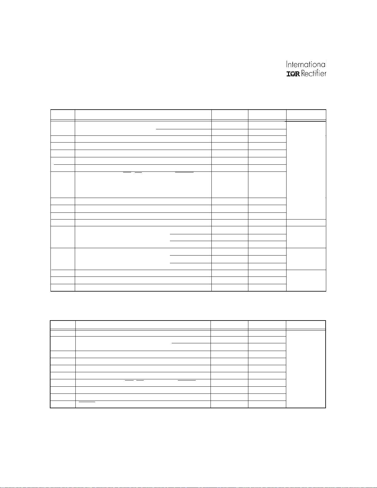
Packages
28-Lead SOIC
44-Lead PLCC w/o 12 leads
28-Lead PDIP
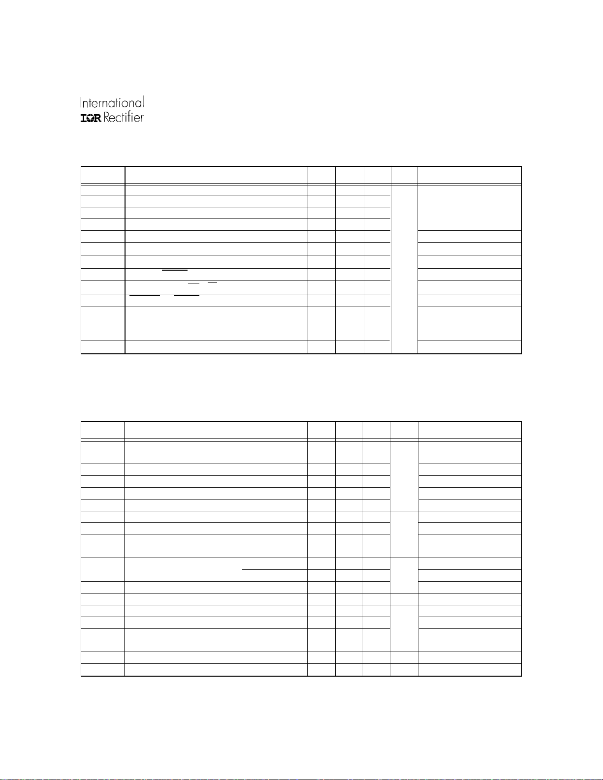
Typical Connection
(Refer to Lead Assignments for correct pin configuration). This/These diagram(s) show electrical connections only.
Please refer to our Application Notes and DesignTips for proper circuit board layout.
www.irf.com 1
up to 600V or 1200V
Page 2
IR2133/IR2135/IR2233/IR2235(J&S
) & (PbF)
Absolute Maximum Ratings
Absolute Maximum Ratings indicate sustained limits beyond which damage to the device may occur. All voltage parameters are absolute voltages referenced to COM. The Thermal Resistance and Power Dissipation
ratings are measured under board mounted and still air conditions.
Symbol Definition Min. Max. Units
V
B1,2,3
High side floating supply voltage (IR2133/IR2135) -0.3 625
(IR2233/IR2235) -0.3 1225
V
V
V
V
V
V
S1,2,3
HO1,2,3
CC
SS
LO1,2,3
IN
High side floating supply offset voltage V
High side floating output voltage V
- 25 V
B1,2,3
- 0.3 V
S1,2,3
B1,2,3
B1,2,3
+ 0.3
+ 0.3
Fixed supply voltage -0.3 25
Logic ground VCC - 25 VCC + 0.3
Low side output voltage -0.3 VCC + 0.3
Logic input voltage (HIN, LIN, ITRIP, SD & FLT-CLR) VSS - 0.3 (VSS + 15) or
(V
+ 0.3)
CC
V
whichever is
lower
V
V
V
dV
P
IN,AMP
OUT,AMP
FLT
D
Op amp input voltage (CA+ & CA-) VSS - 0.3 VCC + 0.3
Op amp output voltage (CAO) VSS - 0.3 VCC + 0.3
output voltage
FAULT
/dt Allowable offset supply voltage transient — 50
S
Package power dissipation @ T
≤ 25ºC (28 Lead PDIP) — 1.5
A
VSS - 0.3 VCC + 0.3
(28 Lead SOIC) — 1.6
V/ns
W
(44 lead PLCC) — 2.0
Rth
(28 Lead SOIC) — 78
Thermal resistance, junction to ambient (28 Lead PDIP) — 83
JA
ºC/W
(44 lead PLCC) — 63
T
J
T
S
T
L
Junction temperature — 125
Storage temperature -55 150
Lead temperature (soldering, 10 seconds — 300
ºC
Recommended Operating Conditions
The input/output logic timing diagram is shown in figure 1. For proper operation the device should be used within the
recommended conditions. All voltage parameters are absolute voltages referenced to COM. The VS offset rating is
tested with all supplies biased at 15V differential.
Symbol Parameter Definition Min. Max. Units
V
B1,2,3
V
S1,2,3
V
HO1,2,3
V
CC
V
SS
V
LO1,2,3
V
IN
V
IN,AMP
V
OUT,AMP
V
FLT
Note 1: Logic operational for VS of COM - 5V to COM + 600V/1200V. Logic state held for VS of COM -5V to COM -VBS. (Please refer to the Design Tip
DT97-3 for more details).
Note 2: All input pins, op amp input and output pins are internally clamped with a 5.2V zener diode.
High side floating supply voltage V
+ 10/12 V
S1,2,3
S1,2,3
High side floating supply offset voltage (IR2133/IR2135) Note 1 600
(IR2233/IR2235) Note 1 1200
High side floating output voltage V
S1,2,3
V
B1,2,3
Fixed supply voltage 10 or 12 20
Low side driver return -5 5
Low side output voltage 0 V
Logic input voltage (HIN, LIN, ITRIP, SD & FLT-CLR) V
Op amp input voltage (CA+ & CA-) V
Op amp output voltage (CAO) V
output voltage
FAULT
V
SS
SS
SS
SS
CC
VSS + 5
VSS + 5
VSS + 5
V
CC
+ 20
V
2 www.irf.com
Page 3
IR2133/IR2135/IR2233/IR2235(J&S
Dynamic Electrical Characteristics
(
V
BIAS
,
V
V
CC
BS1,2,3
)
= 15V, V
S1,2,3
= V
SS
,
TA = 25oC and C
= 1000 pF unless otherwise specified.
L
) & (PbF)
Symbol
t
on
t
off
t
r
t
f
t
sd
t
itrip
t
bl
t
flt
t
fil,in
t
fltclr
Definition Min. Typ. Max. Units Test Conditions
Turn-on propagation delay 500 750 1000
Turn-off propagation delay 450 700 950
Turn-on rise time — 90 150
Turn-off fall time — 40 70
SD to output shutdown propagation delay 500 750 1000 V
ITRIP to output shutdown propagation delay 600 850 1100 V
ITRIP blanking time — 400 — ITRIP = 1V
ITRIP to FAULT propagation delay 400 650 900 V
Input filter time (HIN, LIN and SD) — 310 — V
FLT-CLR to FAULT clear time 600 850 1100 V
DT Deadtime, LS turn-off to HS turn-on & 100 250 400 V
HS turn-off to LS turn-on
SR+ Amplifier slew rate (positive) 5 10 —
SR- Amplifier slew rate (negative) 2 2.5 —
NOTE: For high side PWM, HIN pulse width must be ≥ 1µ sec
Static Electrical Characteristics
V
BIAS
are referenced to V
referenced to COM
Symbol
V
IH
V
IL
V
FCLR,IH
V
FCLR,IL
V
SD,TH
V
SD,TH
V
IT,TH
V
IT,TH
V
OH
V
OL
I
LK
I
QBS
I
QCC
+
I
IN
-
I
IN
I
SD
-
I
SD
I
ITRIP
I
ITRIP
,
(V
CC
V
) = 15V unless otherwise specified and TA = 25oC. All static parameters other than IO and VO
BS1,2,3
and are applicable to all six channels (H
SS
and V
and are applicable to the respective output leads: H
S1,2,3
S1,2,3
& L
). The VO and IO parameters are
S1,2,3
Definition Min. Typ. Max. Units Test Conditions
Logic “0” Input Voltage (OUT = LO) 2.2 — —
Logic “1” Input Voltage (OUT = HI) — — 0.8
Logic “0” Fault Clear Input Voltage 2.2 — —
Logic “1” Fault Clear Input Voltage — — 0.8
+
SD Input Positive Going Threshold 1.6 1.9 2.2
-
SD Input Negative Going Threshold 1.4 1.7 2.0
+
I
Input Positive Going Threshold 470 570 670
ITRIP
-
I
Input Negative Going Threshold 360 460 560
ITRIP
High Level Output Voltage, V
Low Level Output Voltage, V
Offset Supply Leakage Current (IR2133/IR2135) — — 50 V
(IR2233/IR2235) — — 50 V
Quiescent VBS Supply Current — 50 100 VIN = 0V or 5V
Quiescent VCC Supply Current — 4 8 mA VIN = 0V or 5V
Logic “1” Input Bias Current (OUT = HI) — 200 350 VIN = 0V
Logic “0” Input Bias Current (OUT = LO) — 100 250 VIN = 5V
+
“High” Shutdown Bias Current — 30 100 SD = 5V
“Low” Shutdown Bias Current — — 100 nA SD = 0V
+
“High” I
-
“Low” I
Bias Current — 30 100 µA I
ITRIP
Bias Current — — 100 nA I
ITRIP
BIAS
O
- V
O
— — 100 VIN = 0V, IO = 0A
— — 100 VIN = 5V, IO = 0A
ns
V/µs
O1,2,3
V
mV
µA
µA
VIN = 0 & 5V
V
S1,2,3
IN,VSD
IN,VITRIP
IN,VITRIP
= 0 & 5V
IN
IN,VITRIP
= 0 & 5V
IN
or L
O1,2,3.
B1,2,3=VS1,2,3
B1,2,3=VS1,2,3
= 5V
ITRIP
= 0V
ITRIP
= 0 to 600V
or 1200V
= 0 & 5V
= 0 & 5V
= 0 & 5V
= 0 & 5V
= 600V
= 1200V
www.irf.com 3
Page 4
IR2133/IR2135/IR2233/IR2235(J&S
Static Electrical Characteristics — Continued
(V
CC
,
V
) = 15V unless otherwise specified and TA = 25oC. All static parameters other than IO and VO
BS1,2,3
and are applicable to all six channels (H
SS
and V
and are applicable to the respective output leads: H
S1,2,3
V
BIAS
are referenced to V
referenced to COM
) & (PbF)
& L
S1,2,3
). The VO and IO parameters are
S1,2,3
O1,2,3
or L
O1,2,3.
Symbol
I
FLTCLR
I
FLTCLR
V
BSUV
Parameter Definition Min. Typ. Max. Units Test Conditions
+ “High” Fault Clear Input Bias Current — 200 350 FLT-CLR = 0V
- “Low” Fault Clear Input Bias Current — 100 250 FLT-CLR = 5V
+
Supply Undervoltage Positive Going Threshold
V
BS
µA
(for IR2133/IR2233) 7.6 8.6 9.6
(for IR2135/IR2235) 9.2 10.4 11.6
-
V
BSUV
Supply Undervoltage Negative Going Threshold
V
BS
(for IR2133/IR2233) 7.2 8.2 9.2
(for IR2135/IR2235) 8.3 9.4 10.5
V
BSUVHVBS
Supply Undervoltage Lockout Hysteresis
(for IR2133/IR2233) — 0.4 —
(for IR2135/IR2235) — 1 —
V
+
CCUV
Supply Undervoltage Positive Going Threshold
V
CC
V
(for IR2133/IR2233) 7.6 8.6 9.6
(for IR2135/IR2235) 9.2 10.4 11.6
-
V
CCUV
Supply Undervoltage Negative Going Threshold
V
CC
(for IR2133/IR2233) 7.2 8.2 9.2
(for IR2135/IR2235) 8.3 9.4 10.5
V
CCUVHVCC
Supply Undervoltage Lockout Hysteresis
(for IR2133/IR2233) — 0.4 —
(for IR2135/IR2235) — 1 —
R
on,FLT
+
I
O
-
I
O
V
OS
I
IN,AMP
FAULT- Low On Resistance — 70 100
Output High Short Circuit Pulsed Current 200 250 —
Output Low Short Circuit Pulsed Current 420 500 — V
Amplifier Input Offset Voltage — 0 30 mV CA+=0.2V, CA-=CAO
Amplifier Input Bias Current — — 4 nA CA+ = CA- = 2.5V
Ω
mA
= 0V, VIN = 0V
V
OUT
PW ≤ 10
= 15V, VIN = 5V
OUT
PW ≤ 10
µ
s
µ
s
CMRR Amplifier Common Mode Rejection Ratio 50 70 — CA+ = 0.1V & 5V, CA- = CAO
PSRR Amplifier Power Supply Rejection Ratio 50 70 — CA+=0.2V, CA-=CAO
V
OH,Amp
V
OL,Amp
I
SRC,Amp
I
SNK,Amp
I
O+,Amp
I
O-,Amp
Amplifier High Level Output Voltage 5 5.2 5.4 V CA+ = 1V, CA- = 0V
Amplifier Low Level Output Voltage — — 20 mV CA+ = 0V, CA- = 1V
Amplifier Output Source Current 4 7 — CA+ = 1V, CA- = 0V, CAO = 4V
Amplifier Output Sink Current 0.5 1 — CA+ = 0V, CA- = 1V, CAO = 2V
Amplifier Output High Short Circuit Current — 10 — CA+ = 5V, CA- = 0V, CAO = 0V
Amplifier Output Low Short Circuit Current — 4 — CA+ = 0V, CA- = 5V, CAO = 5V
dB
mA
= 10V & 20V
V
CC
4 www.irf.com
Page 5
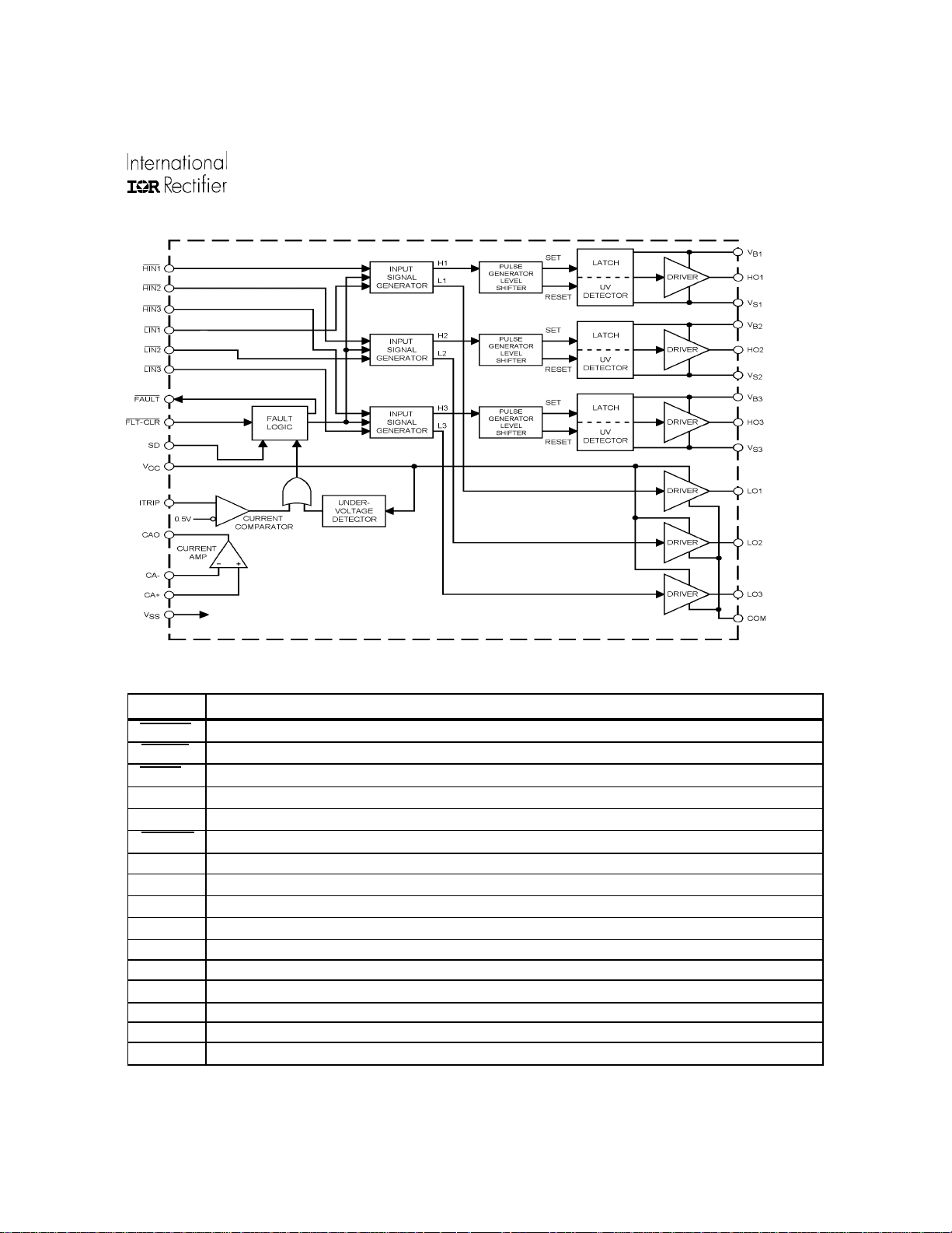
Functional Block Diagram
IR2133/IR2135/IR2233/IR2235(J&S
) & (PbF)
Lead Definitions
Symbol Lead Description
HIN1,2,3 Logic inputs for high side gate driver outputs (HO1,2,3), out of phase.
LIN1,2,3 Logic inputs for low side gate driver outputs (LO1,2,3), out of phase.
FAULT Indicates over-current or undervoltage lockout (low side) has occurred, negative logic.
V
CC
ITRIP Input for over-current shut down.
FLT-CLR Logic input for fault clear, negative logic.
SD Logic input for shut down.
CAO Output of current amplifier.
CA- Negative input of current amplifier.
CA+ Positive input of current amplifier.
V
SS
COM Low side return.
V
B1,2,3
HO1,2,3 High side gate drive outputs.
V
S1,2,3
LO1,2,3 Low side gate drive outputs
www.irf.com 5
Logic and low side fixed supply.
Logic ground.
High side floating supplies.
High side floating supply returns.
Page 6
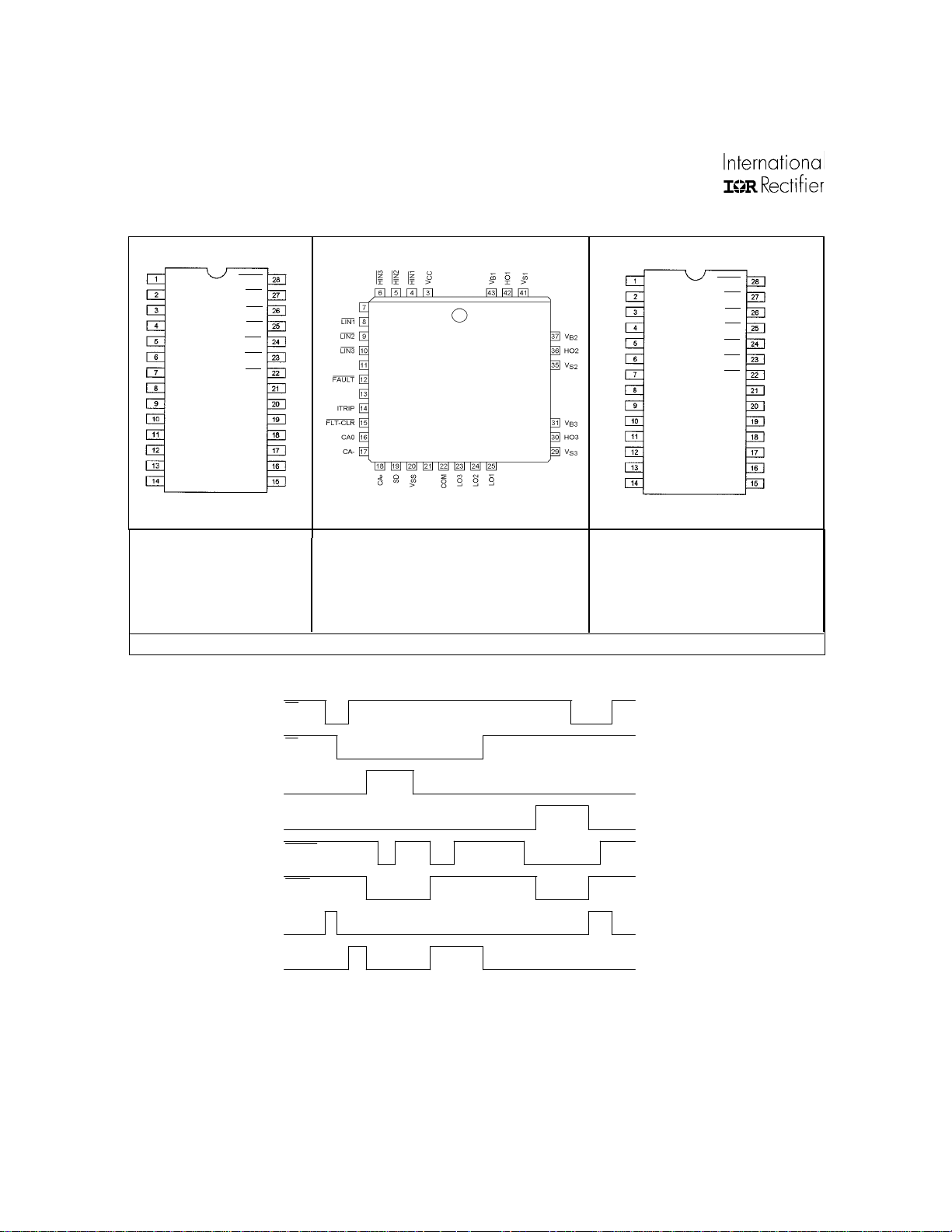
IR2133/IR2135/IR2233/IR2235(J&S
Lead Assignments
) & (PbF)
ITRIP
FLT-CLR
CAO
CA-
CA+
SD
VSS
COM
LO3
LO2
LO1
VS3
HO3
VB3
FAULT
LIN3
LIN2
LIN1
HIN3
HIN2
HIN1
VCC
VB1
HO1
VS1
VB2
HO2
VS2
ITRIP
FLT-CLR
CAO
CA-
CA+
SD
VSS
COM
LO3
LO2
LO1
VS3
HO3
VB3
FAULT
LIN3
LIN2
LIN1
HIN3
HIN2
HIN1
VCC
VB1
HO1
VS1
VB2
HO2
VS2
28 Lead DIP 44 Lead PLCC w/o 12 Leads 28 Lead SOIC (Wide Body)
IR2133
IR2135
IR2133J
IR2135J
IR2233J
IR2235J
IR2133S
IR2135S
IR2233S
IR2235S
Part Number
HIN
LIN
ITRIP
SD
FLT-CLR
FAULT
HO
1,2,3
LO
1,2,3
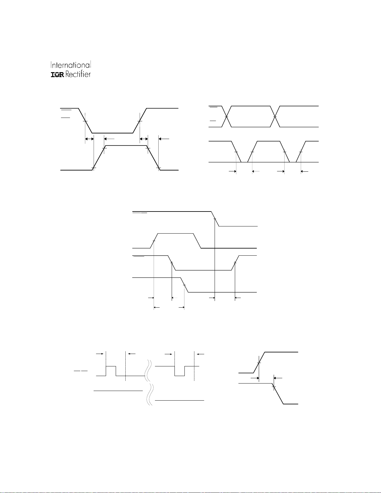
Figure 1. Input/Output Timing Diagram
6 www.irf.com
Page 7
IR2133/IR2135/IR2233/IR2235(J&S
N
) & (PbF)
HIN
LIN
50%
t
on
t
r
50%
t
off
90% 90%
HO
LO
Figure 2. Switching Time Waveform Definitions
10% 10%
FLT-CLR
ITRIP
FAULT
Any Output
HI
50%
50%
LIN
t
f
LO
50% 50%
HO
DT
DT
Figure 3. Deadtime Waveform Definitions
50%
50%
50%
50%
50%
t
flt
t
itrip
t
fltclr
Figure 4. Overcurrent Shutdown Waveform
HIN/LIN
HO/LO
on
t
in,fil
on on off
high
t
in,fil
offoff
low
U
50%
SD
t
sd
HO
90%
LO
Figure 4.5. Input Filter Function Figure 5. Shutdown Waveform Definitions
www.irf.com 7
Page 8
IR2133/IR2135/IR2233/IR2235(J&S
)
)
)
) & (PbF)
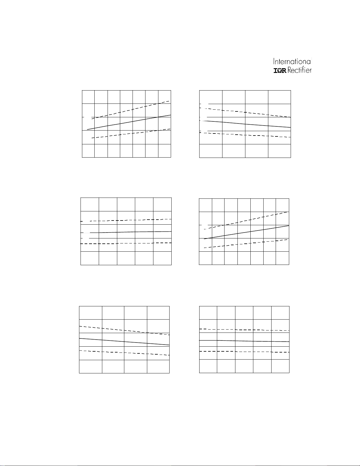
1500
1200
M ax.
900
Typ.
600
Min.
300
Turn-on Delay Time (ns
0
-50-25 0 255075100125
o
Temperature (
C)
Figure 6A. Turn-On Time vs. Temperature
1500
1200
M ax.
900
Typ.
600
Min.
300
Turn-on Delay Time (ns
1500
1200
M ax.
Typ.
900
Min.
600
300
Turn-on Delay Time (ns
0
10 12.5 15 17.5 20
Supply V oltage ( V)
Figure 6B. Turn-On Time vs. Voltage
1500
1200
900
Max.
Typ.
600
Turn-Off Time (ns)
Min.
300
0
2.5 3 3.5 4 4.5 5
Input Voltage (V)
Figure 6C. Turn-On Time vs. Input Voltage
1500
1200
M ax.
900
Typ.
600
Min.
Turn-Off Time (ns)
300
0
10 12.5 15 17.5 20
Supply V oltage (V)
Figure 7B. Turn-Off Tim e vs. V oltage
8 www.irf.com
0
-50 - 25 0 25 50 75 100 125
o
Temperature (
C)
Figure 7A. Turn-Off Time vs. Te mperature
1500
1200
M ax.
900
Typ.
600
Min.
Turn-Off Time (ns)
300
0
2.5 3 3.5 4 4.5 5
Input Voltage (V)
Figure 7C. Turn-Off Time vs. Input
Page 9
IR2133/IR2135/IR2233/IR2235(J&S
e
e
)
)
) & (PbF)
250
200
150
M ax.
100
Typ.
50
Turn-On Rise Time (ns
0
-50 - 25 0 25 50 75 100 125
o
Temperature (
C)
Fiure 8A. Turn-On Rise Time vs.Temper ature
150
120
90
M ax.
60
Turn-Off Fall Tim
Typ.
30
250
200
M ax.
150
Typ.
100
50
Turn-On Rise Time (ns
0
10 12.5 15 17.5 20
Supply Voltage (V)
Fiure 8B. Turn-On Rise Time vs.Voltage
150
120
90
M ax.
60
Turn-Off Fall Tim
Typ.
30
0
-50 - 25 0 25 50 75 100 125
o
Temperature (
C)
Figure 9A. Turn-Off Fall Time vs. Temper ature
1500
1200
M ax.
900
Typ.
600
Min.
300
SD to output SD Time (ns
0
-50-25 0 25 50 75100125
Temperature (
o
C)
Figure 10A. SD to Output shutdow n Time
vs. Te m per atur e
www.irf.com 9
0
10 12.5 15 17.5 20
Supply V oltage (V )
Figure 9B. Turn-Off Fall Time vs. Voltage
1500
M ax.
1200
Typ.
900
Min.
600
300
SD to output SD Time (ns
0
10 12.5 15 17.5 20
Supply Voltage (V )
Figure 10B. SD to Output shutdown Time
vs. V oltage
Page 10

IR2133/IR2135/IR2233/IR2235(J&S
s
s
s
s
s
s
) & (PbF)
1500
1200
900
M ax.
Typ.
600
Min.
300
ITRIP to FAULT Time (n
0
-50-25 0 25 50 75100125
Temperature (
o
C)
_____
Figure 11A. ITRIP to FAULT Time
vs. Te m per atur e
1800
1500
1200
M ax.
900
Typ.
Min.
600
ITRIP to output SD Time (n
300
-50 - 25 0 25 50 75 100 125
Temperature (
o
C)
1500
1200
M ax.
900
Typ.
600
Min.
300
ITRIP to FAULT Time (n
0
10 12.5 15 17.5 20
Supply Voltage (V)
_____
Figure 11B. ITRIP to FAULT Time
vs. V oltage
1800
1500
M ax.
1200
Typ.
900
Min.
600
ITRIP to output SD Time (n
300
10 12.5 15 17.5 20
Supply V oltage (V)
Figure 12A. ITRIP to output shutdow n Tim e
vs. Te m per atur e
1800
1500
1200
M ax.
900
Typ.
Min.
600
300
FLT-CLR to FAULT clear Time (n
-50-25 0 25 50 75100125
Temperature (
________ ______
o
C)
Figure 13A. FLT-CLR to FAULT clear Tim e
10 www.irf.com
vs. Te m per atur e
Figure 12B. ITRIP to output s hutdow n Tim e
vs. V oltage
1800
1500
M ax.
1200
Typ.
900
Min.
600
300
FLT-CLR to FAULT clear Time (n
10 12.5 15 17.5 20
Supply Voltage (V)
________ ______
Figure 13B. FLT-CLR to FAULT clear Time
vs. V oltage
Page 11

IR2133/IR2135/IR2233/IR2235(J&S
) & (PbF)
750
600
450
M ax.
300
Typ.
Deadtime (ns)
150
Min.
0
-50 -25 0 25 50 75 100 125
Temperature (
o
C)
Figure 14A. Deadtime vs. Tem per ature
20
s)
µ
16
12
Typ.
8
Min.
4
Amplifier slew rate (v /
0
-50 - 25 0 25 50 75 100 125
Temperature (
o
C)
750
600
M ax.
450
Typ.
300
Deadtime (ns)
Min.
150
0
10 12.5 15 17.5 20
Supply V oltage (V )
Figure 14B. Deadtim e vs. V oltage
20
s)
µ
16
12
Typ.
8
Min.
4
Amplifier slew rate (v/
0
10 12.5 15 17.5 20
Supply Voltage (V)
Figure 15A. Amplifier slew rate (+)
vs. Temper atu re
5
s)
µ
4
Figure 15B. Amplifier s lew rate (+)
vs. V oltage
5
s)
µ
4
3
Typ.
2
Min.
1
Amplifier slew rate (v /
0
-50-250 255075100125
Temperature (
o
C)
Figure 16A. Amplifier slew rate (-)
vs. Temper ature
3
Typ.
Min.
2
Amplifier slew rate (v/
1
10 12.5 15 17.5 20
Supply Voltage (V)
Figure 16B. Amplifier s le w r ate (-)
vs. Voltage
www.irf.com 11
Page 12

IR2133/IR2135/IR2233/IR2235(J&S
)
)
) & (PbF)
6
5
4
3
Min.
2
Logic "0" Input Voltage (V)
1
-50 - 25 0 25 50 75 100 125
Temperature (
o
C)
Figure 17A. Logic "0" Input Voltage (OUT=LO),
Fault Clear Voltage vs . Tem per atur e
5
4
3
2
M ax.
1
Logic "1" Input Voltage (V)
0
-50 - 25 0 25 50 75 100 125
Temper a tre (
o
C)
6
5
4
3
Min.
2
Logic "0" Input Voltage (V)
1
10 12.5 15 17.5 20
Supply V oltage (V )
Figure 17B. Logic "0" Input Voltage (OUT=LO),
Fault Clear Voltage vs . Voltage
5
4
3
2
M ax.
1
Logic "1" Input Voltage (V)
0
10 12.5 15 17.5 20
Supply V oltage ( V)
Figure 18A. Logic "1" Input (OUT=HI), Fault
Clear Input Voltage vs. Temperature
3.0
2.5
M ax.
Typ.
2.0
Min.
1.5
SD Input TH (+) (V
1.0
-50 - 25 0 25 50 75 100 125
o
Temper a tre (
C)
Figure 21A. SD Input TH(+) vs .
Figure 18B. Logic "1" Input (OUT=HI), Fault
Clear Input V oltage vs . Voltage
3.0
2.5
M ax.
Typ.
2.0
Min.
1.5
SD Input TH (+) (V
1.0
10 12.5 15 17.5 20
Supply Voltage (V )
Figure 21B. SD Input TH(+) vs. Voltage
Tem perature
12 www.irf.com
Page 13

IR2133/IR2135/IR2233/IR2235(J&S
)
)
)
)
)
)
) & (PbF)
3.0
2.5
M ax.
2.0
Typ.
Min.
1.5
SD Input TH (-) (V
1.0
-50 - 25 0 25 50 75 100 125
Temper a tre (
o
C)
Figure 22A. SD Input TH(-) vs. Tem perature
1000
800
M ax.
Typ.
600
Min.
Input TH (+) (mV
400
ITRIP
I
200
-50-25 0 255075100125
o
Temperature (
C)
3.0
2.5
M ax.
2.0
Typ.
Min.
1.5
SD Input TH (-) (V
1.0
10 12.5 15 17.5 20
Supply Voltage (V )
Figure 22B. SD Input TH(-) vs. Voltage
1000
800
Max.
Typ.
600
Min.
Input TH (+) (mV
400
ITRIP
I
200
10 12.5 15 17.5 20
Supply V oltage (V )
Figure 23A. I
900
700
M ax.
500
Typ.
Min.
Input TH (-) (mV
300
ITRIP
I
100
-50 - 25 0 25 50 75 100 125
Figure 24A. I
Input TH(+) vs. Temperature
ITRIP
o
Temperature (
Input TH(-) vs.Temperature
ITRIP
C)
Figure 23B. I
Input TH(+) vs. Voltage
ITRIP
900
700
M ax.
Typ.
500
Min.
Input TH (-) (mV
300
ITRIP
I
100
10 12.5 15 17.5 20
Supply Voltage (V)
Fig u r e 24B. I
Input TH(-) vs. Voltage
ITRIP
www.irf.com 13
Page 14

IR2133/IR2135/IR2233/IR2235(J&S
) & (PbF)
0.5
0.4
0.3
0.2
M ax.
0.1
0.0
-50 - 25 0 25 50 75 100 125
High Level Output Voltage ( V)
Temperature (
o
C)
Figure 25A. High Level Output vs. Temperature
0.5
0.4
0.3
0.2
M ax.
0.1
0
-50 - 25 0 25 50 75 100 125
Low Level Output Voltage ( V)
Temperature (
o
C)
0.5
0.4
0.3
0.2
M ax.
0.1
0.0
10 12.5 15 17.5 20
High Level Output Voltage (V)
Supply Voltage (V)
Figure 25B. High Level Output vs. Voltage
0.5
0.4
0.3
0.2
M ax.
0.1
0
10 12.5 15 17.5 20
Low Level Output Voltage (V)
Supply V oltage (V )
Figure 26A. Low Le vel Output vs. Tempe rature
500
A)
µ
400
300
200
100
M ax.
0
-50 -25 0 25 50 75 100 125
Temperature (
o
C)
Offset Supply Leakage Current (
Figure 27A. Offs et Supply Leakage
Current vs. Temper ature
Figure 26B. Low Level Output vs. V oltage
500
A)
µ
400
300
200
100
M ax.
0
0 100 200 300 400 500 600
Supply V oltage (v)
Offset Supply Leak age Cur rent (
Figure 27B. Offset Supply Le ak age
Curre nt vs. V oltage
14 www.irf.com
Page 15

IR2133/IR2135/IR2233/IR2235(J&S
) & (PbF)
250
)
µΑ
200
150
M ax.
100
Typ.
50
V Supply Curr ent (
0
-50-250 255075100125
Temperature (
o
C)
Figure 28A. VBS Supply Current
vs. Temper ature
20
A)
µ
16
12
M ax.
8
Typ.
Supply Cur rent (
4
cc
V
0
-50-25 0 25 50 75100125
Temperature (
o
C)
250
)
µΑ
200
150
100
M ax.
50
V Supply Curr ent (
Typ.
0
10 12.5 15 17.5 20
Supply V oltage (V)
Figure 28B. VBS Supply Current
vs. V oltage
20
A)
µ
16
12
M ax.
8
Typ.
Supply Current (
4
cc
V
0
10 12.5 15 17.5 20
Supply Voltage (V)
Figure 29A. Vcc Supply Current vs.
Fig u r e 29B. Vcc Supply Curr ent vs. Voltage
Tem perature
800
A)
µ
600
400
M ax.
200
Typ.
Logic "1" Input Current (
0
-50-25 0 25 50 75100125
o
Temperature (
C)
Figure 30A. Logic "1" Input Bais Curr ent
vs. Temperature
800
A)
µ
600
400
M ax.
200
Typ.
Logic "1" Input Current (
0
10 12.5 15 17.5 20
Supply Voltage (V)
Figure 30B. Logic "1" Input Bais Current
vs. Voltage
www.irf.com 15
Page 16

IR2133/IR2135/IR2233/IR2235(J&S
) & (PbF)
800
A)
µ
600
400
200
M ax.
Logic "0" Input Current (
Typ.
0
-50-25 0 25 50 75100125
o
Temperature (
C)
Figure 31A. Logic "0" Input Bais Current
vs. Temper ature
400
A)
µ
300
200
100
M ax.
"High" SD Bais Current (
Typ.
0
-50-25 0 255075100125
o
Temperature (
C)
800
A)
µ
600
400
M ax.
200
Typ.
Logic "0" Input Current (
0
10 12.5 15 17.5 20
Supply V oltage ( V)
Figure 31B. Logic "0" Input Bais Current
vs. Supply Voltage
400
A)
µ
300
200
M ax.
100
Typ.
"High" SD Bais Current (
0
10 12.5 15 17.5 20
Supply V oltage (V)
Figure 32A. "High" Shutdown Bais Current
vs. Temper atu re
500
400
300
200
M ax.
100
"Low" SD Bais Current (nA)
0
-50 -25 0 25 50 75 100 125
Temperature (
o
C)
Figure 33A. "Low" Shutdown Bais Curr ent
vs. Temper ature
Figure 32B. "High" Shutdown Bais Current
vs. Supply Voltage
500
400
300
200
M ax.
100
"Low" SD Bais Curren t ( nA)
0
10 12.5 15 17.5 20
Supply V oltage (V )
Figure 33B. "Low" Shutdown Bais Curre nt
vs. Supply Voltage
16 www.irf.com
Page 17

IR2133/IR2135/IR2233/IR2235(J&S
) & (PbF)
400
A)
µ
300
200
Bias Cur rent (
ITRIP
100
M ax.
"High" I
Typ.
0
-50 -25 0 25 50 75 100 125
o
Temperature (
Figure 34A. "High" I
vs. Temperature
C)
Bais Cur rent
ITRIP
500
400
300
Bais Current (nA)
200
M ax.
ITRIP
100
"Low" I
0
-50-250 255075100125
Temperature (
o
C)
400
A)
µ
300
200
Bias Current (
M ax.
ITRIP
100
Typ.
"High" I
0
10 12.5 15 17.5 20
Supply Voltage (V)
Figure 34B. "High" I
vs. Supply Voltage
Bais Curre nt
ITRIP
500
400
300
Bais Current (nA)
200
M ax.
ITRIP
100
"Low" I
0
10 12.5 15 17.5 20
Supply Voltage (V)
Figure 35A. "Low" I
vs. Temperature
800
A)
µ
600
400
M ax.
200
Typ.
0
-50-25 0 25 50 75100125
"High" Fault Clear Input Current (
Temperature (
Figure 36A. "High" Fault Clear Input Bais Current
vs. Temper atu re
Bais Cur rent
ITRIP
o
C)
Figure 35B. "Low" I
vs. Supply Voltage
800
A)
µ
Bais Curre nt
ITRIP
600
400
M ax.
200
Typ.
0
10 12.5 15 17.5 20
"High" F ault Clear Input Curr ent (
Supply V oltage (V)
Figure 36B. "High" Fault Clear Input Bais Current
vs. Supply voltage
www.irf.com 17
Page 18

IR2133/IR2135/IR2233/IR2235(J&S
) & (PbF)
800
A)
µ
600
400
200
M ax.
Typ.
0
-50-25 0 25 50 75100125
"Low" Fault Clear Input Current (
o
Temperature (
C)
Figure 37A. "Low " Fault Clear Input Bais Curre nt
vs. Temper ature
14
12
M ax.
Typ.
10
Min.
UV Th (+) (V)
BS
V
8
6
-50 -25 0 25 50 75 100 125
o
Temperature (
C)
800
A)
µ
600
400
200
M ax.
Typ.
0
10 12.5 15 17.5 20
"Low" Fault Clear Input Current (
Supply V oltage ( V)
Figure 37B. "Low" Fault Clear Input Bais Curre nt
vs. Supply Voltage
12
11
M ax.
9
Typ.
UV Th (+) (V)
Min.
BS
8
V
6
-50 -25 0 25 50 75 100 125
o
Temperature (
C)
Figure 38A. IR2135/IR2235 VBS Undervoltage
Threshold (+) vs. Tem pe rature
14
12
M ax.
10
Typ.
Min.
V UV TH (+) (V)
8
6
-50 - 25 0 25 50 75 100 125
Temperature (
o
C)
Figur e 39A. IR2135/IR2235 VBS Undervoltage
Threshold (-) vs. Tem perature
Figure 38B. IR2133/IR2233 VBS Undervoltage
Threshold (+) vs. Temperature
12
11
M ax.
9
Min.
Typ.
V UV TH (+) (V)
8
6
-50 -25 0 25 50 75 100 125
o
Temperature (
C)
Figur e 39B. IR2133/IR2233 VBS Undervoltage
Threshold (-) vs. Temperature
18 www.irf.com
Page 19

IR2133/IR2135/IR2233/IR2235(J&S
) & (PbF)
14
13
M ax.
11
Typ.
UV TH (+) (V)
cc
Min.
10
V
8
-50 - 25 0 25 50 75 100 125
o
Temperature (
Figur e 40A. IR2135/IR2235 V
Thre shold (+) vs. Temper ature
C)
Undervoltage
cc
12
M ax.
11
Typ.
9
Min.
UV TH (+) (V)
cc
8
V
6
-50 - 25 0 25 50 75 100 125
Temperature (
o
C)
12
11
M ax.
9
Typ.
UV TH (+) (V)
Min.
cc
8
V
6
-50-25 0 25 50 75100125
o
Temperature (
Figur e 40B. IR2133/IR2233 V
Threshold (+) vs. Te mperature
C)
Undervoltage
cc
12
11
M ax.
9
Typ.
UV TH (+) (V)
cc
8
Min.
V
6
-50 - 25 0 25 50 75 100 125
Temperature (
o
C)
Figur e 41A. IR2135/IR2235 Vcc Undervoltage
Threshold (-) vs. Tem perature
200
Ω)
150
100
M ax.
Typ.
50
0
FAULT-Low O n Res istance (
-50 - 25 0 25 50 75 100 125
Temperature (oC)
Figure 42A. FAULT- Low On Resistance
vs. Temper atu re
Figur e 41B. IR2133/IR2233 Vcc Undervoltage
Threshold (-) vs. Temperature
)
150
Ω
120
M ax.
90
Typ.
60
30
0
FAULT-Low On Resistance (
10 12.5 15 17.5 20
Supply Voltage (V )
Figure 42B. FAULT- Low On Resistance
vs. Supply Voltage
www.irf.com 19
Page 20

IR2133/IR2135/IR2233/IR2235(J&S
) & (PbF)
500
)
Α
400
Typ.
300
Min.
200
100
Output Source Current (m
0
-50 - 25 0 25 50 75 100 125
Temperature (
o
C)
Figure 43A. Output Source Current
vs. Temperature
1000
)
Α
800
Typ.
600
Min.
400
200
Output Sink Current (m
0
-50 -25 0 25 50 75 100 125
Temperature (
o
C)
500
)
Α
400
300
Typ.
200
Min.
100
Output Source Curr ent (m
0
10 12.5 15 17.5 20
Supply v oltage ( V)
Figure 43B. Output Source Curr ent
vs. Supply Voltage
1000
)
Α
800
600
Typ.
Min.
400
200
Output Sink Current (m
0
10 12.5 15 17.5 20
Supply V oltage (V)
Figure 44A. Ourput Sink Current
vs. Temper ature
90
70
50
M ax.
30
10
Typ.
-10
Amplifier Input O ff set Voltage (mV)
-50 - 25 0 25 50 75 100 125
Temperature (
o
C)
Figure 45A. Am plifier Input Offest Voltage
vs. Temperature
90
70
50
30
10
-10
Amplifier Input Offset Voltage (mV)
Figure 44B. Ourput Sink Current
vs. Supply Voltage
M ax.
Typ.
10 12.5 15 17.5 20
Supply Voltage (V)
Figure 45B. Amplifier Input Offest Voltage
vs. Supply Voltage
20 www.irf.com
Page 21

IR2133/IR2135/IR2233/IR2235(J&S
)
) & (PbF)
150
120
90
Typ.
Min.
60
30
Amplifier CMRR (dB)
0
-50 - 25 0 25 50 75 100 125
Temperature (
o
C)
Figure 46A. Amplifier Comm on Mode Rejection
Ratio vs. Temperature
125
100
Typ.
75
Min.
50
Amplifier PSRR ( dB)
25
0
-50 - 25 0 25 50 75 100 125
Temperature (
o
C)
150
120
90
Typ.
Min.
60
30
Amplifier CMRR (dB
0
10 12.5 15 17.5 20
Supply V oltage (V )
Figure 46B. Amplifier Com mon Mode Rejection
Ratio vs. Supply Voltage
125
100
Typ.
75
Min.
50
Amplifier PSRR (dB)
25
0
10 12.5 15 17.5 20
Supply Voltage (V)
Figure 47A. Amplifier Power Supply Rejection
Ratio vs. Tem perature
6.0
5.7
(V)
M ax.
OH
5.4
Typ.
Min.
5.1
Amplifier V
4.8
4.5
10 12.5 15 17.5 20
Supply V oltage (V)
Figure 48. Amplifier High Level Output Voltage
vs. Supply Voltage
Figure 47B. Amplifier Pow er Supply Re jection
Ratio vs. Supply Voltage
50
40
(V)
OL
30
M ax.
20
Amplifier V
10
0
10 12.5 15 17.5 20
Supply V oltage (V )
Figure 49. Amplifier Low Level Output Voltage
vs. Supply Voltage
www.irf.com 21
Page 22

IR2133/IR2135/IR2233/IR2235(J&S
) & (PbF)
15
(V)
12
SRC
9
6
Typ.
Min.
3
Amplifier I
0
10 12.5 15 17.5 20
Supply V oltage (V)
Figure 50. Amplifier Output Source Current
vs. Supply Voltage
20
16
+ (V)
O
12
8
Typ.
4
Amplifier I
0
10 12.5 15 17.5 20
Supply V oltage (V )
2.5
(V)
2.0
SNK
1.5
Typ.
1.0
Min.
0.5
Amplifier I
0.0
10 12.5 15 17.5 20
Supply V oltage (V)
Figure 51. Am plifier Output Sink Curre nt
vs. Supply Voltage
20
16
- (V)
O
12
8
Typ.
4
Amplifier I
0
10 12.5 15 17.5 20
Supply Voltage (V)
Figure 52. Amplifier Output High Short Circuit
Current vs. Supply Voltage
Figure 53. Amplifier Output Low Short Circuit
Curre nt vs. Supply Voltage
22 www.irf.com
Page 23

IR2133/IR2135/IR2233/IR2235(J&S
) & (PbF)
120
110
100
90
80
70
60
50
40
30
Juntion Tem per at ur e (°C )
20
1E+2 1E+3 1E+4 1E+5
Frequency (Hz)
Figure 7. IR2133J Junction Temperature vs
Frequency Driving (IRGPC20KD2) Rgate = 5.1Ω @
Vcc = 15V
120
110
100
90
80
70
60
50
40
30
Junct ion Tem per at ur e (°C )
20
1E+2 1E+3 1E+4 1E+5
Frequency (Hz)
Figure 9. IR2133J Junction Temperature vs
Frequency Driving (IRGPC40KD2) Rgate = 5.1Ω @
Vcc = 15V
480V
320V
160V
0V
480V
320V
160V
0V
120
110
100
90
80
70
60
50
40
30
Juntion Tem per ature ( °C)
20
1E+2 1E+3 1E+4 1E+5
Frequency (Hz)
Figure 8. IR2133J Junction Temperature vs
Frequency Driving (IRGPC30KD2) Rgate = 5.1Ω @
Vcc = 15V
150
140
130
120
110
100
90
80
70
60
50
40
30
Ju n ction Tem per at ur e (°C)
20
1E+2 1E+3 1E+4 1E+5
Frequency (Hz)
Figure 10. IR2133J Junction Temperature vs
Frequency Driving (IRGPC50KD2) Rgate = 5.1Ω @
Vcc = 15V
480
320V
160
0V
480V
320V
160V
0V
www.irf.com 23
Page 24

IR2133/IR2135/IR2233/IR2235(J&S
1
1
1
) & (PbF)
120
900V
110
100
500
90
80
70
300V
60
50
40
30
Junction Tem perature (°C )
20
0V
1E+2 1E+3 1E+4 1E+5
Frequency (Hz)
Figure 11. IR2233J Junction Temperature vs
Frequency Driving (IRG4PH30KD) Rgate = 20Ω @
Vcc = 15V
500V
900V
120
110
300V
100
90
80
70
60
50
40
30
Ju nction Tem perature (°C )
20
0V
1E+2 1E+3 1E+4 1E+5
Frequency (Hz)
Figure 13. IR2233J Junction Temperature vs
Frequency Driving (IRG4PH50KD) Rgate = 10Ω @
Vcc = 15V
120
110
100
90
80
70
60
50
40
30
Junction Tem per atur e ( °C)
20
1E+2 1E+3 1E+4 1E+5
Frequency (Hz)
Figure 12. IR2233J Junction Temperature vs
Frequency Driving (IRG4PH40KD) Rgate = 15Ω @
Vcc = 15V
900V
120
110
100
90
80
70
60
50
40
30
Ju nction Tem perature (°C )
20
1E+2 1E+3 1E+4 1E+5
Frequency (Hz)
Figure 14. IR2233J Junction Temperature vs
Frequency Driving (IRG4ZH71KD) Rgate = 5Ω @
Vcc = 15V
900V
300V
500V
500V
300
0V
0V
24 www.irf.com
Page 25

Package Dimensions
IR2133/IR2135/IR2233/IR2235(J&S
) & (PbF)
28-Lead PDIP (wide body)
28-Lead SOIC (wide body)
NOTES
01-3024 02
01-3040 02
01-6011
(MS-011AB)
01-6013
(MS-013AE)
www.irf.com 25
Page 26

IR2133/IR2135/IR2233/IR2235(J&S
) & (PbF)
44-Lead PLCC w/o 12 leads
26 www.irf.com
01-3004 02(mod.
01-6009 00
) (MS-018AC)
Page 27

IR2133/IR2135/IR2233/IR2235(J&S
LEADFREE PART MARKING INFORMATION
) & (PbF)
Part number
Date code
Pin 1
Identifier
?
P
IRxxxxxx
YWW?
MARKING CODE
Lead Free Released
Non-Lead Free
Released
ORDER INFORMATION
Basic Part (Non-Lead Free)
28-Lead PDIP IR2133 order IR2133 2
8-Lead SOIC IR2133S order IR2133S
28-Lead PDIP IR2135 order IR2135
28-Lead SOIC IR2135S order IR2135S
28-Lead PDIP IR2233 not available
28-Lead SOIC IR2233S order IR2233S
28-Lead PDIP IR2235 not available
28-Lead SOIC IR2235S order IR2235S
44-Lead PLCC IR2133J order IR2133J
44-Lead PLCC IR2135J order IR2135J
44-Lead PLCC IR2233J order IR2233J
44-Lead PLCC IR2235J order IR2235J
IR logo
?XXXX
Lot Code
(Prod mode - 4 digit SPN code)
Assembly site code
Per SCOP 200-002
Leadfree Part
28-Lead PDIP IR2133 order IR2133PbF
28-Lead SOIC IR2133S order IR2133SPbF
28-Lead PDIP IR2135 order IR2135PbF
28-Lead SOIC IR2135S order IR2135SPbF
28-Lead PDIP IR2233 order IR2233PbF
28-Lead SOIC IR2233S order IR2233SPbF
28-Lead PDIP IR2235 order IR2235PbF
28-Lead SOIC IR2235S order IR2235SPbF
44-Lead PLCC IR2133J order IR2133JPbF
44-Lead PLCC IR2135J order IR2135JPbF
44-Lead PLCC IR2233J order IR2233JPbF
44-Lead PLCC IR2235J order IR2235JPbF
IR WORLD HEADQUARTERS: 233 Kansas St., El Segundo, California 90245 Tel: (310) 252-7105
Data and specifications subject to change without notice. 9/22/2005
www.irf.com 27
This product has been qualified per industrial level
 Loading...