

Page 1
查询IR2122供应商
Preliminary Data Sheet No. PD60130-J
CURRENT SENSING SINGLE CHANNEL DRIVER
Features
• Floating channel designed for bootstrap operation
Fully operational to +600V
T olerant to negative transient v oltage
dV/dt immune
• Gate drive supply range from 10 to 20V
• Undervoltage lockout
• 3.3V , 5V and 15V input logic compatib le
FAULT
•
• Output out of phase with input
Description
The IR2122(S) is a high voltage, high speed power
MOSFET and IGBT driver. Proprietary HVIC and latch
immune CMOS technologies enable ruggedized
monolithic construction. The logic input is compatible
with standard CMOS or LSTTL outputs, down to
3.3V. The protection circuity detects over-current in
the driven power transistor and terminates the gate
drive voltage. An open drain
vided to indicate that an over-current shutdown has
occurred. The output driver features a high pulse
current buffer stage designed for minimum cross-conduction. The floating channel can be used to drive an
N-channel power MOSFET or IGBT in the high side
or low side configuration which operates up to 600
volts.
lead indicates shutdown has occured
FAULT
signal is pro-
Product Summary
V
OFFSET
+/- 110 mA / 110 mA
I
O
V
OUT
V
CSth
t
(typ.) 250 & 200 ns
on/off
Packages
8-Lead PDIP
IR2122(S
600V max.
10 - 20V
500 mV
8-Lead SOIC
)
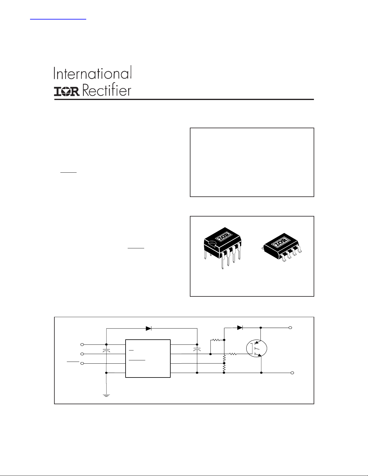
Typical Connection
V
CC
IN
FAULT
www.irf.com 1
V
CC
IN
FAULT
COM
V
B
HO
CS
V
S
(Refer to Lead Assignments for correct pin configuration). This/These
diagram(s) show electrical connections only. Please refer to our
Application Notes and DesignTips for proper circuit board layout.
Page 2
IR2122(S)
Absolute Maximum Ratings
Absolute Maximum Ratings indicate sustained limits beyond which damage to the device may occur. All voltage parameters are absolute voltages referenced to COM. The Thermal Resistance and Power Dissipation ratings are measured
under board mounted and still air conditions.
Symbol Definition Min. Max. Units
V
B
V
S
V
HO
V
CC
V
IN
V
FLT
V
CS
dVs/dt Allowable Offset Supply Voltage Transient — 50 V/ns
P
D
R
THJA
T
J
T
S
T
L
High Side Floating Supply Voltage -0.3 625
High Side Floating Offset Voltage VB - 25 VB + 0.3
High Side Floating Output Voltage VS - 0.3 V
B
+ 0.3
Logic Supply Voltage -0.3 25 V
Logic Input Voltage -0.3 V
Output Voltage -0.3 V
FAULT
Current Sense Voltage VS - 0.3 V
CC
CC
B
+ 0.3
+ 0.3
+ 0.3
Package Power Dissipation @ TA ≤ +25°C (8 Lead DIP) — 1.0
(8 Lead SOIC) — 0.625
Thermal Resistance, Junction to Ambient (8 Lead DIP) — 125
(8 Lead SOIC) — 200
°C/W
Junction Temperature — 150
Storage Temperature -55 150
°C
Lead Temperature (Soldering, 10 seconds) — 300
W
Recommended Operating Conditions
The Input/Output logic timing diagram is shown in Figure 1. For proper operation the device should be used within the
recommended conditions. The VS offset rating is tested with all supplies biased at 15V differential.
Symbol Definition Min. Max. Units
V
B
V
S
V
HO
V
CC
V
IN
V
FLT
V
CS
T
A
Note 1: Logic operational f or VS of -5 to +600V. Logic state held f or VS of -5V to -VBS. (Please refer to the Design Tip
DT97-3 for more details).
2 www.irf.com
High Side Floating Supply Voltage VS + 13 VS + 20
High Side Floating Offset Voltage Note 1 600
High Side Floating Output Voltage V
S
V
B
Logic Supply Voltage 13 20 V
Logic Input Voltage 0 V
Output Voltage 0 V
FAULT
Current Sense Signal Voltage V
S
CC
CC
V
+ 5
S
Ambient Temperature -40 150 °C
Page 3

IR2122(S)
Dynamic Electrical Characteristics
V
(VCC, VBS) = 15V, CL = 1000 pF and TA = 25°C unless otherwise specified. The dynamic electrical characteristics
BIAS
are measured using the test circuit shown in Figure 3.
Symbol Definition Min. Typ. Max. Units Test Conditions
t
on
t
off
t
t
t
bl
t
cs
t
flt
Static Electrical Characteristics
V
(VCC, VBS) = 15V and TA = 25°C unless otherwise specified. The VIN, VTH and IIN parameters are referenced to
BIAS
COM. The VO and IO parameters are referenced to VS.
Symbol Definition Min. Typ. Max. Units Test Conditions
V
V
V
CSTH+
V
OH
V
OL
I
LK
I
QBS
I
QCC
I
IN+
I
IN-
I
CS+
I
CS-
V
BSUV+
V
BSUV-
I
O+
I
O-
Turn-On Propagation Delay — 250 — V
Turn-Off Propagation Delay — 200 — V
Turn-On Rise Time — 250 — C
r
Turn-Off Fall Time — 250 — C
f
ns
Start-Up Blanking Time 500 9 00 —
CS Shutdown Propagation Delay — 350 —
CS to
Logic “0” Input Voltage (OUT = LO) 3.0 —— VCC = 10V to 20V
IH
Logic “1” Input Voltage (OUT = HI) ——0.8 VCC = 10V to 20V
IL
CS Input Positive Going Threshold 350 500 650 VCC = 10V to 20V
High Level Output Voltage, V
Pull-Up Propagation Delay — 450 —
FAULT
- VO ——100 IO = 0A
BIAS
V
Low Level Output Voltage, VO ——100 mV IO = 0A
Offset Supply Leakage Current ——50 VB = VS = 600V
Quiescent VBS Supply Current — 150 350 VIN = 0V or 5V
Quiescent VCC Supply Current — 60 120 VIN = 0V or 5V
Logic “1” Input Bias Current — 7.0 15 µA V
Logic “0” Input Bias Current ——1.0 VIN = 5V
“High” CS Bias Current ——1.0 VCS = 3V
“High” CS Bias Current ——1.0 VCS = 0V
VBS Supply Undervoltage Positive Going 10.0 11.4 13.0
Threshold
VBS Supply Undervoltage Negative Going 9.5 10.4 12.5
V
Threshold
Output High Short Circuit Pulsed Current 110
Output Low Short Circuit Pulsed Current 110
130
130
— VO = 0V, V
mA
— VO = 15V, V
= 0V
S
= 600V
S
= 1000 pF
L
= 1000 pF
L
= 0V
IN
IN
PW ≤ 10 µs
IN
PW ≤ 10 µs
= 0V
= 5V
www.irf.com 3
Page 4

IR2122(S)
Functional Block Diagram
Lead Definitions
Lead
Symbol Description
V
CC
IN
FAULT
COM Logic ground
V
B
HO
V
S
CS
Logic and gate drive supply
Logic input for gate driver output (HO), out of phase with HO
Indicates over-current shutdown has occurred, negative logic
High side floating supply
High side gate drive output
High side floating supply return
Current sense input to current sense comparator
Lead Assignments
8 Lead PDIP 8 Lead SOIC
IR2122 IR2122S
4 www.irf.com
Page 5

IR2122(S)
www.irf.com 5
Page 6

IR2122(S)
Case outlines
A
87
6
E
e
6X
0.25 [.010] C A B
NOTES:
1. DIMENS IONING & TOLERANCING PER ASME Y14.5M- 1994.
2. CONTROLLING DIMENSION: MILLIMETER
3. DIMENS IONS ARE SHOWN IN MILLIMETE RS [INCHES ].
4. OUT LINE CONFORMS TO JEDEC OUTLINE MS-012AA.
D B
5
65
4312
e1
8X b
A1
H
0.25 [.010] A
A
C
0.10 [.004]
8-Lead PDIP
6.46 [.255]
3X 1.27 [.050]
y
FOOTPRINT
8X 0.72 [.028]
K x 45°
8X L
8X 1.78 [.070]
8X c
01-3003 01
DIM
MIN MAX
.0688
.0532
A
A1
b
c .0075 .0098 0.19 0.25
D
E
e
e1
H
K
L
y
.0098
.0040
.020
.013
.1968
.189
.1574
.1497
.050 BASIC
.025 BASIC 0.635 BASIC
.2440
.2284
.0196
.0099
.050
.016
8°
0°
7
5 DIMENSION DOES NOT INCLUDE MOLD PROT RUSIONS.
MOLD PROTRUSIONS NOT TO EXCEED 0.15 [.006] .
6 DIMENSION DOES NOT INCLUDE MOLD PROT RUSIONS.
MOLD PROTRUSIONS NOT TO EXCEED 0.25 [.010] .
7 DIMENSION IS THE LE NGTH OF LEAD FOR SOLDERING TO
A SUBSTRATE.
8-Lead SOIC
01-0021 11
IR WORLD HEADQUARTERS: 233 Kansas St., El Segundo, California 90245 Tel: (310) 252-7105
Data and specifications subject to change without notice. 5/15/2001
01-6014
(MS-001AB)
MILLIMETERSINCHES
MIN MAX
1.35
1.75
0.10
0.25
0.33
0.51
4.80
5.00
3.80
4.00
1.27 BA SIC
5.80
6.20
0.25
0.50
0.40
1.27
0°
8°
01-6027
(MS-012AA)
6 www.irf.com
 Loading...