

Page 1
查询IR2117PBF供应商
Data Sheet No. PD60146 Rev N
IR2117(S)/IR2118(S) & ( PbF)
SINGLE CHANNEL DRIVER
Features
Floating channel designed for bootstrap operation
•
Fully operational to +600V
Tolerant to negative transient voltage
dV/dt immune
Gate drive supply range from 10 to 20V
•
Undervoltage lockout
•
CMOS Schmitt-triggered inputs with pull-down
•
• Output in phase with input (IR2117) or out of
phase with input (IR2118)
Also available LEAD-FREE
•
Description
The IR2117/IR2118(S) is a high voltage, high speed
power MOSFET and IGBT driver. Proprietary HVIC and
latch immune CMOS technologies enable ruggedized
monolithic construction. The logic input is compatible
with standard CMOS outputs. The output driver features a high pulse current buffer stage designed for
minimum cross-conduction. The floating channel can
be used to drive an N-channel power MOSFET or IGBT
in the high or low side configuration which operates up
to 600 volts.
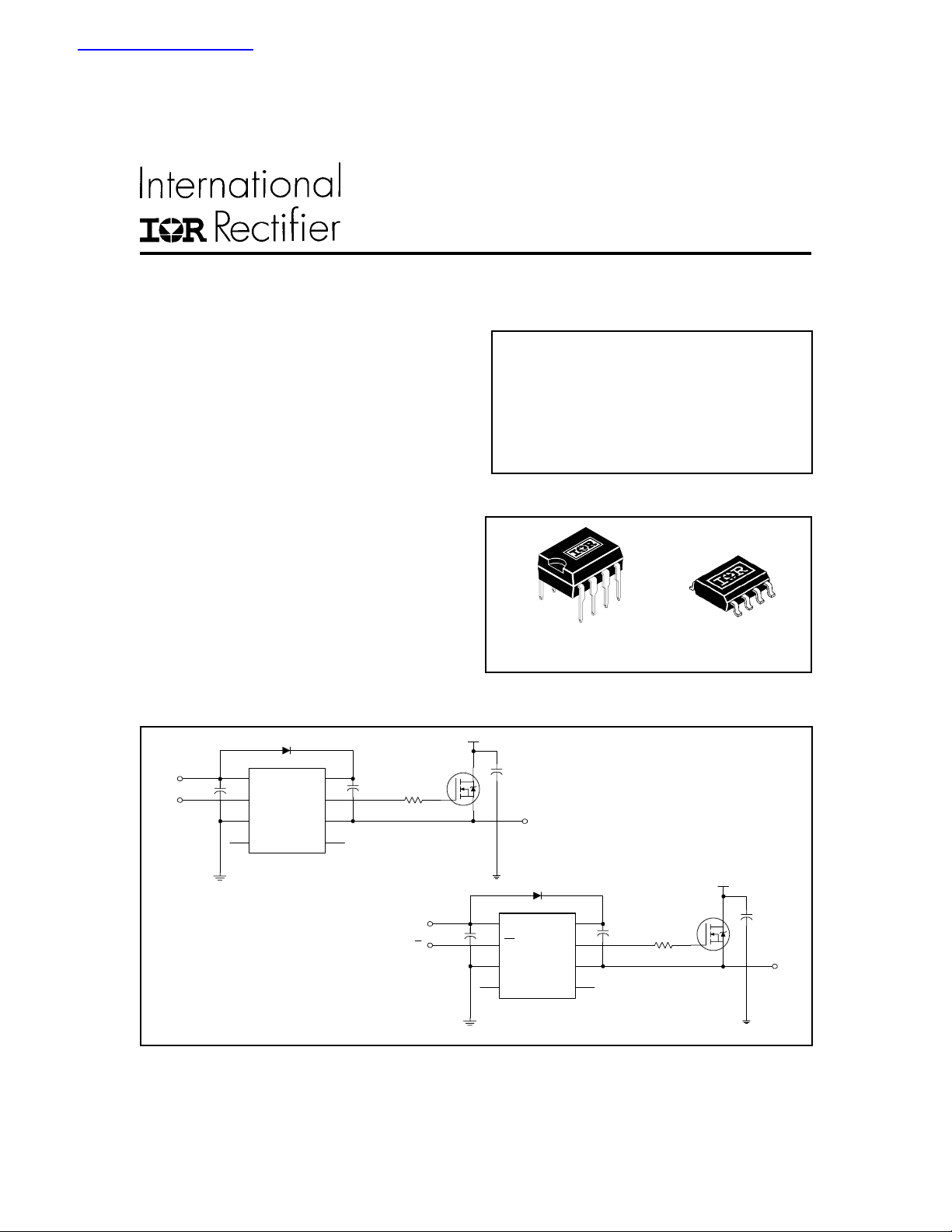
Typical Connection
Product Summary
V
OFFSET
+/- 200 mA / 420 mA
I
O
V
OUT
t
(typ.) 125 & 105 ns
on/off
Packages
8-Lead PDIP
IR2117/IR2118
up to 600V
600V max.
10 - 20V
8-Lead SOIC
IR2117S/IR2118S
V
CC
IN
V
CC
COM
V
B
HOIN
V
S
TO
LOAD
IR2117
up to 600V
(Refer to Lead Assignments for correct pin configuration).
This/These diagram(s) show electrical connections only.
Please refer to our Application Notes and DesignTips for
proper circuit board layout.
V
CC
IN
V
CC
COM
V
B
HOIN
V
S
IR2118
TO
LOAD
www.irf.com 1
Page 2
IR2117(S)/IR2118(S) & ( PbF)
Absolute Maximum Ratings
Absolute maximum ratings indicate sustained limits beyond which damage to the device may occur. All voltage parameters are absolute voltages referenced to COM. The thermal resistance and power dissipation ratings are measured
under board mounted and still air conditions. Additional information is shown in Figures 5 through 8.
Symbol Definition Min. Max. Units
V
B
V
S
V
HO
V
CC
V
IN
dVs/dt Allowable offset supply voltage transient (figure 2) — 50 V/ns
P
D
Rth
JA
T
J
T
S
T
L
High side floating supply voltage -0.3 625
High side floating supply offset voltage VB - 25 VB + 0.3
CC
B
+ 0.3
+ 0.3
High side floating output voltage VS - 0.3 V
Logic supply voltage -0.3 25
Logic input voltage -0.3 V
Package power dissipation @ TA ≤ +25°C (8 lead PDIP) — 1.0
(8 lead SOIC) — 0.625
Thermal resistance, junction to ambient (8 lead PDIP) — 125
(8 lead SOIC) — 200
Junction temperature — 150
Storage temperature -55 150
Lead temperature (soldering, 10 seconds) — 300
W
°C/W
°C
V
Recommended Operating Conditions
The input/output logic timing diagram is shown in figure 1. For proper operation the device should be used within the
recommended conditions. The VS offset rating is tested with all supplies biased at 15V differential.
Symbol Definition Min. Max. Units
V
B
V
S
V
HO
V
CC
V
IN
T
A
Note 1: Logic operational for VS of -5 to +600V. Logic state held for VS of -5V to -VBS. (Please refer to the Design Tip
DT97-3 for more details).
2 www.irf.com
High side floating supply absolute voltage VS + 10 VS + 20
High side floating supply offset voltage Note 1 600
High side floating output voltage V
Logic supply voltage 10 20
Logic input voltage 0 V
Ambient temperature -40 125 °C
S
V
B
CC
V
Page 3
IR2117(S)/IR2118(S) & ( PbF)
Dynamic Electrical Characteristics
V
(VCC, VBS) = 15V, CL = 1000 pF and TA = 25°C unless otherwise specified. The dynamic electrical characteristics
BIAS
are measured using the test circuit shown in Figure 3.
Symbol Definition Min. Typ. Max. Units Test Conditions
t
on
t
off
t
t
Static Electrical Characteristics
V
(VCC, VBS) = 15V and TA = 25°C unless otherwise specified. The VIN, VTH and IIN parameters are referenced to
BIAS
COM. The VO and IO parameters are referenced to COM and are applicable to the respective output leads: HO or LO.
Symbol Definition Min. Typ. Max. Units Test Conditions
V
IH
V
V
OH
V
OL
I
LK
I
QBS
I
QCC
I
IN+
I
IN-
V
BSUV+
V
BSUV-
V
CCUV+VCC
V
CCUV-
I
O+
I
O-
Turn-on propagation delay — 125 200 VS = 0V
Turn-off propagation delay — 105 180 VS = 600V
Turn-on rise time — 80 130
r
Turn-off fall time — 40 65
f
input voltage - logic “1” (IR2117) logic “0” (IR2118) 9.5 — —
Input voltage - logic “0” (IR2117) logic “1” (IR2118) — — 6.0
IL
High level output voltage, V
Low level output voltage, V
BIAS
O
- V
O
— — 100 IO = 0A
— — 100 IO = 0A
ns
V
mV
Offset supply leakage current — — 50 VB = VS = 600V
Quiescent VBS supply current — 50 240 V
Quiescent VCC Supply Current — 70 340 VIN = 0V or V
Logic “1” input bias current (IR2117) VIN = V
(IR2118) VIN = 0V
Logic “0” input bias current (IR2117) VIN = 0V
(IR2118) VIN = V
— 20 40
— — 1.0
µA
VBS supply undervoltage positive going threshold 7.6 8.6 9.6
VBS supply undervoltage negative going threshold 7.2 8.2 9.2
V
supply undervoltage positive going threshold 7.6 8.6 9.6
V
supply undervoltage negative going threshold 7.2 8.2 9.2
CC
Output high short circuit pulsed current 200 250 — VO = 0V
Output low short circuit pulsed current 420 500 — VO = 15V
mA
= 0V or V
IN
V
= Logic “1”
IN
PW ≤ 10 µs
V
= Logic “0”
IN
PW ≤ 10 µs
CC
CC
CC
CC
www.irf.com 3
Page 4
IR2117(S)/IR2118(S) & ( PbF)
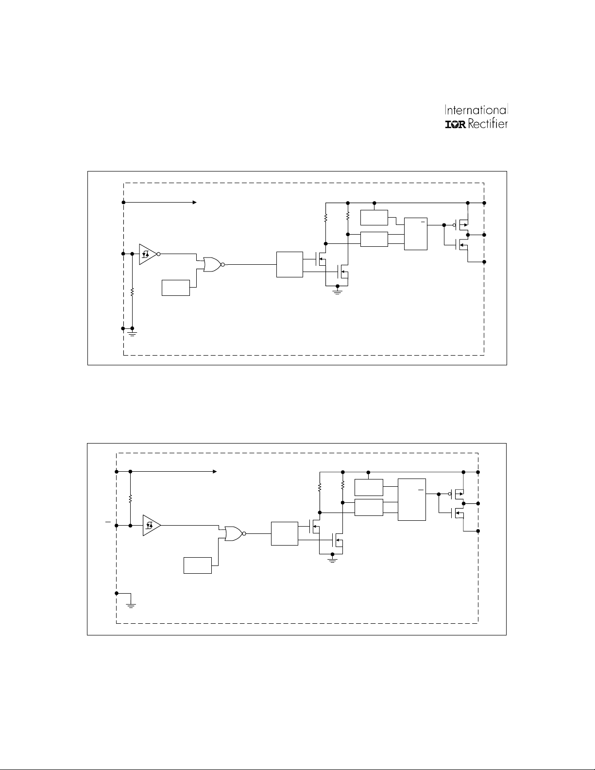
Functional Block Diagram (IR2117)
V
CC
COM
IN
UV
DETECT
PULSE
GEN
Functional Block Diagram (IR2118)
V
CC
IN
PULSE
GEN
LEVEL
HV
LEVEL
SHIFT
HV
SHIFT
UV
DETECT
PULSE
FILTER
UV
DETECT
PULSE
FILTER
V
B
R
Q
R
S
R
Q
R
S
V
HO
V
HO
V
S
B
S
UV
DETECT
COM
4 www.irf.com
Page 5
IR2117(S)/IR2118(S) & ( PbF)
Lead Definitions
Symbol Description
V
CC
IN Logic input for gate driver output (HO), in phase with HO (IR2117)
IN Logic input for gate driver output (HO), out of phase with HO (IR2118)
COM Logic ground
V
B
HO High side gate drive output
V
S
Lead Assignments
Logic and gate drive supply
High side floating supply
High side floating supply return
1
V
CC
2
IN
3
COM
4
V
HO
V
8
B
7
6
S
5
1
2
IN
3
COM
4
8 Lead PDIP 8 Lead SOIC
IR2117 IR2117S
1
V
CC
2
IN
3
COM
4
8 Lead PDIP 8 Lead SOIC
V
HO
V
8
B
7
6
S
5
1
V
2
IN
3
COM
4
IR2118 IR2118S
V
CC
CC
V
HO
V
V
HO
V
8
B
7
6
S
5
8
B
7
6
S
5
www.irf.com 5
Page 6
IR2117(S)/IR2118(S) & ( PbF)
IN
(IR2118)
IN
(IR2117)
HO
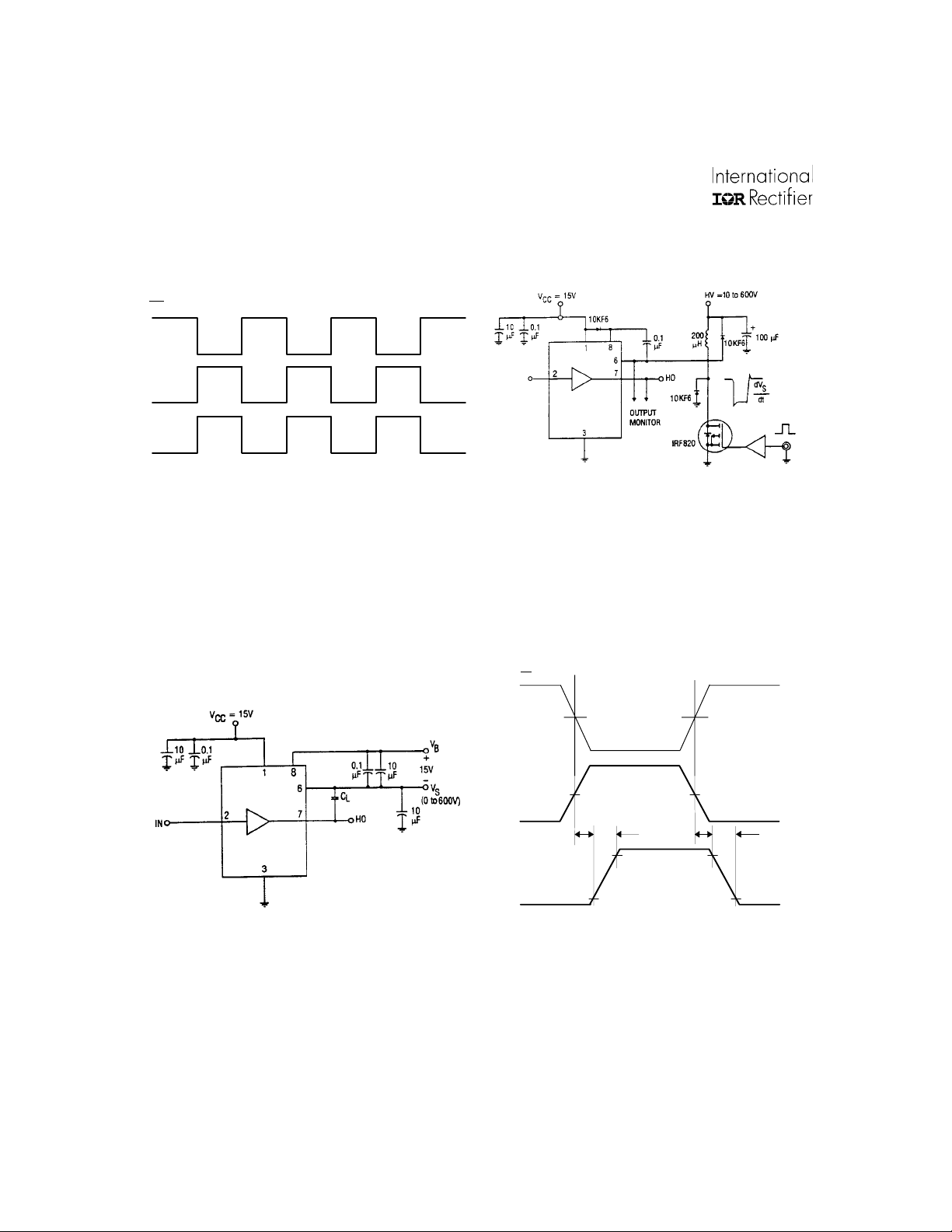
Figure 1. Input/Output Timing Diagram
IR2117/IR2118
IR2117/IR2118
<50 V/ns
Figure 2. Floating Supply Voltage Transient Test Circuit
IN
(IR2118)
50%
50%
50%50%
IN
(IR2117)
t
t
r
on
90% 90%
t
t
f
off
HO
10% 10%
Figure 3. Switching Time Test Circuit Figure 4. Switching Time Waveform Definition
6 www.irf.com
Page 7

IR2117(S)/IR2118(S) & ( PbF)
)
)
p
500
400
300
200
M ax.
100
Typ.
Turn-on Delay Time (ns
0
-50-25 0 25 50 75100125
Temperature (
o
C)
Figure 4A. Turn-On Time
vs. Tem
erature
500
400
500
400
300
M ax.
200
Typ.
100
Turn-on Delay Time (ns
0
10 12 14 16 18 20
V
Supply Voltage (V)
BIAS
Figure 4B. Turn-On Time
vs. Supply Voltage
500
400
300
200
M ax.
Turn-Off Time (ns)
100
Typ.
0
-50-250 255075100125
o
Temperature (
C)
Figure 5A . Turn-Off Time
vs. Temperature
www.irf.com 7
300
M ax.
200
Typ.
Turn-Off Time (ns)
100
0
10 12 14 16 18 20
Supply Voltage (V)
V
BIAS
Figure 5B. Turn-Off Time
vs. Supply Voltage
Page 8

IR2117(S)/IR2118(S) & ( PbF)
)
p
)
pply
)
)
p
500
400
300
200
M ax.
100
Turn-On Rise Time (ns
Typ.
0
-50-250 255075100125
Temperature (
o
C)
F iure 6A . Turn-On Rise Time
vs.Tem
erature
250
200
500
400
300
200
M ax.
100
Turn-On Rise Time (ns
Typ.
0
10 12 14 16 18 20
V
Supply Voltage (V)
BIAS
F igure 6B. Turn-On Rise Time
vs. Su
Voltage
250
200
150
100
M ax.
50
Turn-Off Fall Time (ns
Typ.
0
-50 -25 0 25 50 75 100 125
Temperature (
Figure 7A. Turn-Off Fall Time
vs. Tem
erature
o
C)
150
100
M ax.
50
Turn-Off Fall Time (ns
Typ.
0
10 12 14 16 18 20
Supply Voltage (V)
V
BIAS
Figure 7B. Turn-Off Fall Time
vs. Supply Voltage
8 www.irf.com
Page 9

IR2117(S)/IR2118(S) & ( PbF)
13
12
11
10
Min.
Input Voltage (V)
9
8
-50 -25 0 25 50 75 100 125
Temperatur e (
o
C)
Figure 8A. Logic "1" (IR2118 "0") Input Voltage
vs. Temperature
9
8
13
12
11
10
Min.
Input Voltage (V)
9
8
10 12 14 16 18 20
V
Supply Voltage (V)
cc
Figure 8B. Logic "1" (IR2118 "0") Input Voltage
vs. Supply Voltage
9
8
7
M ax.
6
Input Voltage (V)
5
4
-50-250 255075100125
o
Temperatre (
C)
Figure 9A . Logic " 0" (IR211 8 "1" ) Input Voltage
vs. Temperature
7
M ax.
6
Input Voltage (V)
5
4
10 12 14 16 18 20
Supply Voltage (V)
V
cc
Figure 9B. Logic "0" (IR2118 "1") Input Voltage
vs. Supply Voltage
www.irf.com 9
Page 10

IR2117(S)/IR2118(S) & ( PbF)
)
0.5
0.4
0.3
0.2
M ax.
0.1
High Level Output Voltage (V
0.0
-50 -25 0 25 50 75 100 125
Temperature (
o
C)
Figure 10A. High Level Output
vs. Temperature
0.5
0.4
0.5
0.4
0.3
0.2
M ax.
0.1
High Level Output Voltage (V)
0
10 12 14 16 18 20
V
Supply Voltage (V)
cc
F igure 10B. High Level Output
vs. S upply Voltage
0.5
0.4
0.3
0.2
M ax.
0.1
Low Level Output Voltage (V)
0
-50-250 255075100125
Temperature (oC)
Figure 11 A. Low Level Output
vs.Temperature
0.3
0.2
MAX.
0.1
Low Level Output Voltage (V)
0
10 12 14 16 18 20
V
Supply Voltage (V)
cc
Figure 11B . Low Level Output
vs. Supply Voltage
10 www.irf.com
Page 11

IR2117(S)/IR2118(S) & ( PbF)
500
400
300
200
100
M ax.
0
-50 -25 0 25 50 75 100 125
Offset Supply Leakage Current ( A)
Temperature (
o
C)
F igure 12A. Offset Supply Leakage Current
vs. Temperature
1000
800
500
400
300
200
100
M ax.
0
0 100 200 300 400 500 600
Offset Supply Leakage Current ( A)
V
Boost Voltage (V)
B
Figure 12B. Offset Supply Leakage
Cu rrent vs. V
B
Boost Voltage
1000
800
600
400
M ax.
200
V Supply Current ( )
Typ.
0
-50 -25 0 25 50 75 100 125
o
Temperature (
C)
Figure 13A. VBS Supply Current
vs. Temperature
600
400
M ax.
200
V Supply Current ( )
Typ.
0
10 12 14 16 18 20
V
Supply Voltage (V)
BS
Figure 13B. VBS Supply Current
vs. Supply Voltage
www.irf.com 11
Page 12

IR2117(S)/IR2118(S) & ( PbF)
1000
800
600
400
M ax.
Supply Current ( A)
200
cc
V
Typ.
0
-50-25 0 25 50 75100125
o
Temperature (
C)
Figure 14A. Vcc Supply Current
vs. Temperature
120
100
80
1000
800
600
400
Supply Current ( )
cc
V
M ax.
200
Typ.
0
10 12 14 16 18 20
V
Supply Voltage (V)
cc
Figure 14B. Vcc Supply Current
vs . Su pply Voltage
120
100
80
60
40
M ax.
20
Logic "1" Input Current ( )
Typ.
0
-50 -25 0 25 50 75 100 125
o
Temperature (
C)
Figure 15A. Logic "1" (2118 "0") Input C urrent
vs. Temperature
60
M ax.
40
Typ.
20
Logic "1" Input Current ( )
0
10 12 14 16 18 20
Supply Voltage (V)
V
cc
F igure 15B. Logic "1" (2118 "0") Input Current
vs. S upply Voltage
12 www.irf.com
Page 13

IR2117(S)/IR2118(S) & ( PbF)
5
4
3
2
M ax.
1
Logic "0" Input Current ( )
0
-50 -25 0 25 50 75 100 125
Temperature (
o
C)
F igure 16A. Logic "0" (2118"1") Input Current
vs. Temperature
16
14
5
4
3
2
M ax.
1
Logic "0" Input Current ( )
0
10 12 14 16 18 20
V
Supply Voltage (V)
cc
F igure 16B. Logic "0" (2118"1") Input Current
vs. S upply Voltage
16
14
12
M ax.
10
Typ.
Supply Current ( )
8
cc
Min.
V
6
-50 -25 0 25 50 75 100 125
o
C)
F i gure 17A. V
Temperature (
Undervoltage Threshold (+)
cc
vs. Temperature
12
10
Max
Supply Current ( )
V
Typ.
8
cc
Min.
6
-50 -25 0 25 50 75 100 125
Temperature (
o
C)
Figure 18A. Vcc Undervoltage Threshold (-)
vs. Temperature
www.irf.com 13
Page 14

IR2117(S)/IR2118(S) & ( PbF)
.
16
14
12
Max.
10
Typ.
Supply Current ( )
8
BS
V
Min.
6
-50 -25 0 25 50 75 100 125
Temperature (
o
C)
Figure 19A. VBS Undervoltage Threshold (+)
vs. Temperature
500
400
Typ.
300
16
14
12
M ax.
10
Typ
8
V Supply Current ( )
Min.
6
-50 -25 0 25 50 75 100 125
o
Temperature (
C)
Figure 20A. VBS Undervoltage Threshold (-)
vs. Temperature
500
400
300
200
Min.
100
Output Source Current ( )
0
-50 -25 0 25 50 75 100 125
o
Temperature (
C)
Figure 21A. Output Source Current
vs. Temperature
200
Typ.
100
Min.
Output Source Current ( )
0
10 12 14 16 18 20
V
Supply Voltage (V)
BIAS
Figure 21B. Output Source Current
vs. Supply Voltage
14 www.irf.com
Page 15

IR2117(S)/IR2118(S) & ( PbF)
1000
800
Typ.
600
Min.
400
200
Output Sink Current ( )
0
-50-25 0 25 50 75100125
Temperature (
o
C)
F igure 22A. Output Sink Current
v s.Temperature
0
-2
Typ.
-4
1000
800
600
Typ.
400
Min.
200
Output Sink Current ( )
0
10 12 14 16 18 20
V
Supply Voltage (V)
BIAS
F igure 22B. Output Sink Current
vs. S upply Voltage
-6
-8
-10
vs Offset Supply Voltage (V)
-12
10 12 14 16 18 20
V
Floting Supply Voltage (V)
BS
Figure 23B. Maximum VS Negative Offset
vs. Supply Voltage
www.irf.com 15
Page 16

IR2117(S)/IR2118(S) & ( PbF)
150
125
100
75
50
Junction Temperature (°C)
25
0
1E+2 1E+3 1E+4 1E+5 1E+6
Frequency (Hz)
320V
Figure 24. IR2117/IR2118 TJ vs. Frequency (IRFBC20)
ΩΩ
= 33
Ω, VCC = 15V
ΩΩ
320V
140V 10V
150
125
R
GATE
140V
10V
150
125
100
75
50
Junction Temperature (°C)
25
0
1E+2 1E+3 1E+4 1E+5 1E+6
Frequency (Hz)
Figure 25. IR2117/IR2118 TJ vs. Frequency (IRFBC30)
ΩΩ
= 22
Ω, VCC = 15V
ΩΩ
150
125
R
GATE
320V
140V
10V
320V
140V
10V
100
75
50
Junction Temperature (°C)
25
0
1E+2 1E+3 1E+4 1E+5 1E+6
Frequency (Hz)
Figure 26. IR2117/IR2118 TJ vs. Frequency (IRFBC40)
R
GATE
ΩΩ
= 15
Ω, VCC = 15V
ΩΩ
100
75
50
Junction Temperature (°C)
25
0
1E+2 1E+3 1E+4 1E+5 1E+6
Frequency (Hz)
Figure 27. IR2117/IR2118 TJ vs. Frequency (IRFPE50)
R
GATE
ΩΩ
= 10
Ω, VCC = 15V
ΩΩ
16 www.irf.com
Page 17

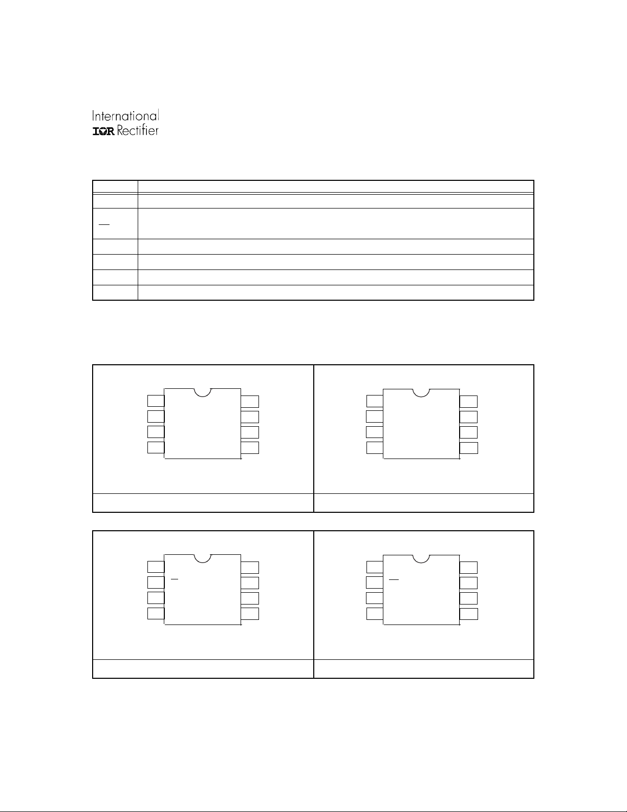
Case outlines
IR2117(S)/IR2118(S) & ( PbF)
A
87
6
E
e
6X
0.25 [ . 01 0] C A B
NOTES:
1. DIMENSIONING & TOLERANCI NG PER ASME Y14.5M-1994.
2. CONTROLLI NG DIMENSION: MILLIMETER
3. DIMENSIONS ARE SHOW N IN MILLIMETERS [INCHES].
4. OUT LINE CONFORMS TO JEDEC OUTLINE MS-01 2 AA .
D B
5
65
4312
e1
8X b
A1
H
0.25 [ . 01 0] A
A
C
0.10 [ . 00 4]
8-Lead PDIP
6.46 [.255]
3X 1.27 [.050]
y
8-Lead SOIC
01-3003 01
DIM
FOOTPRINT
8X 0.72 [.028]
8X 1.78 [.070]
MIN MAX
A
.0532
A1
b
c .0075 .0098 0.19 0.25
D
E
e
e1
H
K
L
y
.0688
.0040
.0098
.013
.020
.189
.1968
.1497
.1574
.050 BASIC
.025 BASIC 0.635 BASIC
.2284
.2440
.0099
.0196
.016
.050
0°
K x 45°
8X L
8X c
7
5 DIMENSION DOES NOT I N CLUDE MOLD PROTRUSIONS.
MOLD PROTRUSIONS NOT TO EXCEED 0.15 [.006].
6 DIMENSION DOES NOT I N CLUDE MOLD PROTRUSIONS.
MOLD PROTRUSIONS NOT TO EXCEED 0.25 [.010].
7 DIMENSI ON IS THE LENGTH OF LEAD FOR SOL DE RING TO
A SU BSTRATE.
8°
01-6014
(MS-001AB)
MILLIMETERSINC H E S
MIN MAX
1.35
1.75
0.10
0.25
0.33
0.51
4.80
5.00
3.80
4.00
1.27 BASIC
5.80
6.20
0.25
0.50
0.40
1.27
8°
0°
01-6027
www.irf.com 17
Page 18

IR2117(S)/IR2118(S) & ( PbF)
LEADFREE PART MARKING INFORMATION
Part number
Date code
Pin 1
Identifier
?
MARKING CODE
Lead Free Released
P
Non-Lead Free
Released
IRxxxxxx
YWW?
ORDER INFORMATION
Basic Part (Non-Lead Free)
8-Lead PDIP IR2117 order IR2117
8-Lead PDIP IR2118 order IR2118
8-Lead SOIC IR2117S order IR2117S
8-Lead SOIC IR2118S order IR2118S
IR logo
?XXXX
Lot Code
(Prod mode - 4 digit SPN code)
Assembly site code
Per SCOP 200-002
Leadfree Part
8-Lead PDIP IR2117 order IR2117PbF
8-Lead PDIP IR2118 order IR2118PbF
8-Lead SOIC IR2117S order IR2117SPbF
8-Lead SOIC IR2118S order IR2118SPbF
IR WORLD HEADQUARTERS: 233 Kansas St., El Segundo, California 90245 Tel: (310) 252-7105
Data and specifications subject to change without notice. 4/2/2004
18 www.irf.com
This product has been qualified per industrial level
 Loading...