

Page 1
查询IR2114SS供应商
Data Sheet No. PD60213 revC
IR2114SS/ IR21141SS
HALF-BRIDGE GATE DRIVER IC
Features
• Floating channel up to +600 or +1200V
• Soft over-current shutdown
• Synchronization signal to synchronize shut down with the other phases
• Integrated desaturation detection circuit
• Two stage turn on output for di/dt control
• Separate pull-up/pull-down output drive pins
• Matched delay outputs
• Under voltage lockout with hysteresis band
Description
The IR2114/21141/2214/IR22141 gate driver family is suited to drive a single
half bridge in power switching applications. The high gate driving capability (2A
source, 3A sink) and the low quiescent current enable bootstrap supply
techniques in medium power systems. These drivers feature full short circuit
protection by means of the power transistor desaturation detection and manages
all the half-bridge faults by turning off smoothly the desaturated transistor
through the dedicated soft shut down pin, therefore preventing over-voltages and
reducing EM emissions. In multi-phase system IR2114/21141/2214/IR22141
drivers communicate using a dedicated local network (SY_FLT and FAULT/SD
signals) to properly manage phase-to-phase short circuits. The system controller
may force shutdown or read device fault state through the 3.3 V compatible
CMOS I/O pin (FAULT/SD). To improve the signal immunity from DC-bus noise,
the control and power ground use dedicated pins enabling low-side emitter
current sensing as well. Undervoltage conditions in floating and low voltage
circuits are managed independently.
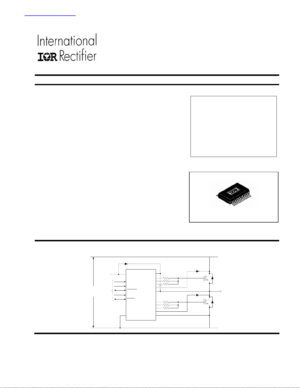
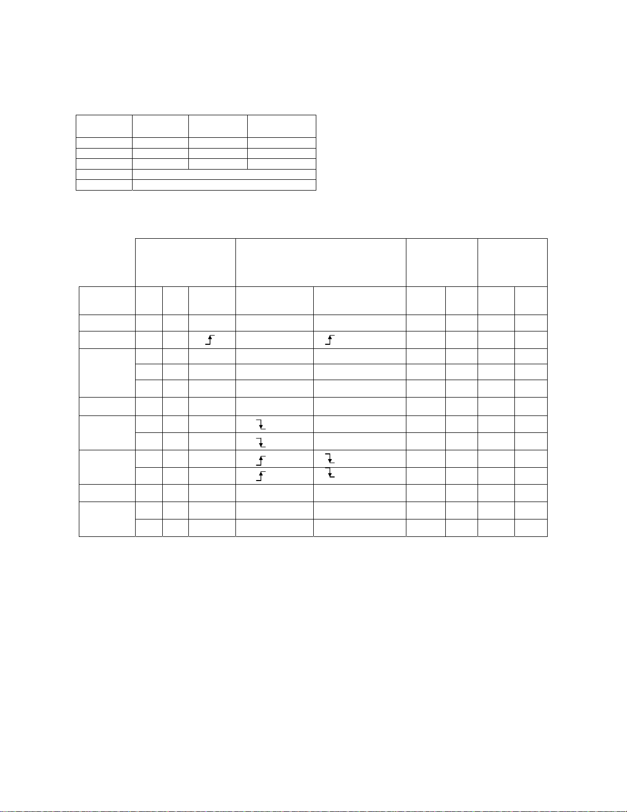
IR2214SS/IR22141SS
Product Summary
V
OFFSET
IO+/- (typ) 2.0 A / 3.0A
V
10.4V - 20V
OUT
Deadtime matching (max) 75 nsec
Deadtime (typ) 330 nsec
Desat blanking time (typ) 3 µsec
DSH, DSL input voltage
threshold (typ)
Soft shutdown time (typ) 9.25 µsec
Package
24-Lead SSOP
600V or
1200V max.
8.0 V
Typical connection
DC BUS
(1200V)
15 V
uP,
Control
VCC
LIN
HIN
FAULT/SD
FLT_CLR
SY_FLT
VSS
IR2214
HOP
HON
SSDH
DSH
LOP
LON
SSDL
COM
DC+
VB
DC-
Motor
VS
DSL
1
Page 2
IR2114/IR21141/IR2214/IR22141
Absolute Maximum Ratings
Absolute maximum ratings indicate sustained limits beyond which damage to the device may occur. All
voltage parameters are absolute voltages referenced to V
The thermal resistance and power dissipation ratings are measured under board mounted and still air
conditions.
Symbol Definition Min. Max. Units
VS High side offset voltage VB - 25 VB + 0.3
VB High side floating supply voltage
VHO High side floating output voltage (HOP, HON and SSDH) VS - 0.3 VB + 0.3
VCC Low side and logic fixed supply voltage -0.3 25
COM Power ground VCC - 25 VCC + 0.3
VLO Low side output voltage (LOP, LON and SSDL) VCOM -0.3 VCC + 0.3
VIN Logic input voltage (HIN, LIN and FLT_CLR) VSS -0.3 VCC + 0.3
VFLT FAULT input/output voltage (FAULT/SD and SY_FLT) VSS -0.3 VCC + 0.3
VDSH High side DS input voltage VS -3 VB + 0.3
VDSL Low side DS input voltage VCOM -3 VCC + 0.3
dVs/dt Allowable offset voltage slew rate — 50 V/ns
PD Package power dissipation @ TA +25°C — 1.5 W
RthJA Thermal resistance, junction to ambient — 65 °C/W
TJ Junction temperature — 125
TS Storage temperature -55 150
TL Lead temperature (soldering, 10 seconds) — 300
SS, all currents are defined positive into any lead
(IR2114 or IR21141)
(IR2214 or IR22141)
-0.3 625
-0.3 1225
V
°C
Recommended Operating Conditions
For proper operation the device should be used within the recommended conditions. All voltage parameters
are absolute voltages referenced to V
differential.
Symbol Definition Min. Max. Units
VB High side floating supply voltage (Note 1) VS + 11.5 VS + 20
VS High side floating supply offset
voltage
VHO High side output voltage (HOP, HON and SSDH) VS VS + 20
VLO Low side output voltage (LOP, LON and SSDL) VCOM VCC
VCC Low side and logic fixed supply voltage (Note 1) 11.5 20
COM Power ground -5 5
VIN Logic input voltage (HIN, LIN and FLT_CLR) VSS VCC
VFLT Fault input/output voltage (FAULT/SD and SY_FLT) VSS VCC
VDSH High side DS pin input voltage VS - 2.0 VB
VDSL Low side DS pin input voltage VCOM - 2.0 VCC
TA Ambient temperature -40 125 °C
Note 1: While internal circuitry is operational below the indicated supply voltages, the UV lockout disables
the output drivers if the UV thresholds are not reached.
Note 2: Logic operational for V
V
SS-VBS. (Please refer to the Design Tip DT97-3 for more details).
S from VSS-5V to VSS+600V or 1200V. Logic state held for VS from VSS-5V to
SS. The VS offset rating is tested with all supplies biased at 15V
(IR2114 or IR21141)
(IR2214 or IR22141)
Note 2 600
Note 2 1200
V
2
Page 3
IR2114/IR21141/IR2214/IR22141
Static Electrical Characteristics
= 15 V, VSS = COM = 0 V, VS = 0 ÷ 600V or 1200 V and TA = 25 °C unless otherwise specified.
V
CC
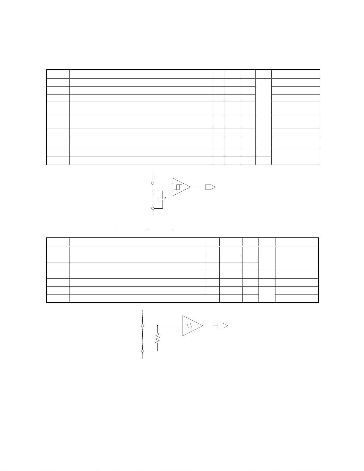
Pin: V
Symbol Definition Min Typ Max Units Test Conditions
VCCUV+ Vcc supply undervoltage positive going threshold 9.3 10.2 11.4
VCCUV- Vcc supply undervoltage negative going threshold 8.7 9.3 10.3
VCCUVH Vcc supply undervoltage lockout hysteresis - 0.9 -
VBSUV+ (VB-VS) supply undervoltage positive going threshold 9.3 10.2 11.4 VS=0V, VS=600V
VBSUV- (VB-VS) supply undervoltage negative going
VBSUVH (VB-VS) supply undervoltage lockout hysteresis - 0.9 -
IQCC Quiescent Vcc supply current - 0.7 2.5
, VSS, VB, VS
CC
V
or 1200V
8.7 9.3 10.3 VS=0V, VS=600V
threshold
or 1200V
ILK Offset supply leakage current - - 50 VB = VS = 600V or
µA
IQBS Quiescent VBS supply current - 400 800
1200V
V
IN = 0V or 3.3V
mA (No load)
VCC/VB
comparator
internal
UV
signal
VCCUV/VBSUV
VSS/VS
Figure 1: Undervoltage diagram
Pin: HIN, LIN, FLTCLR, FAULT/SD, SY_FLT
Symbol Definition Min Typ Max Units Test Conditions
VIH Logic "1" input voltage 2.0 - VIL Logic "0" input voltage - - 0.8
VIHSS
IIN+ Logic "1" input bias current - 370 -
IIN- Logic "0" input bias current -1 - 0
RON,FLT FAULT/SD open drain resistance - 60 -
RON,SY SY_FLT open drain resistance - 60 -
Logic input hysteresis 0.2 0.4 -
CC = VCCUV- to
V
V
µA
20V
V
IN = 3.3V
V
IN = 0V
PW 7 µs
schmitt
HIN/LIN/
FLTCLR
VSS
trigger
10k
internal
signal
Figure 2: HIN, LIN and FLTCLR diagram
3
Page 4
IR2114/IR21141/IR2214/IR22141
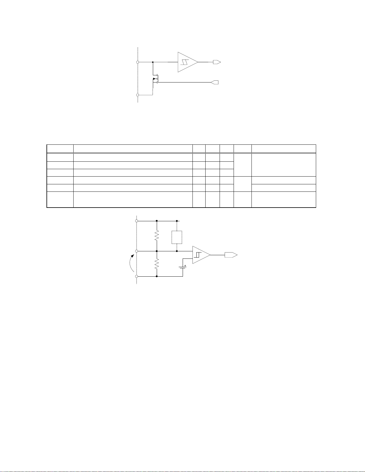
FAULT/SD
SY_FLT
VSS
RON
schmitt
trigger
fault/hold
inte rnal signa l
hard/s oft shut down
inte rnal signa l
Figure 3: FAULT/SD and SY_FLT diagram
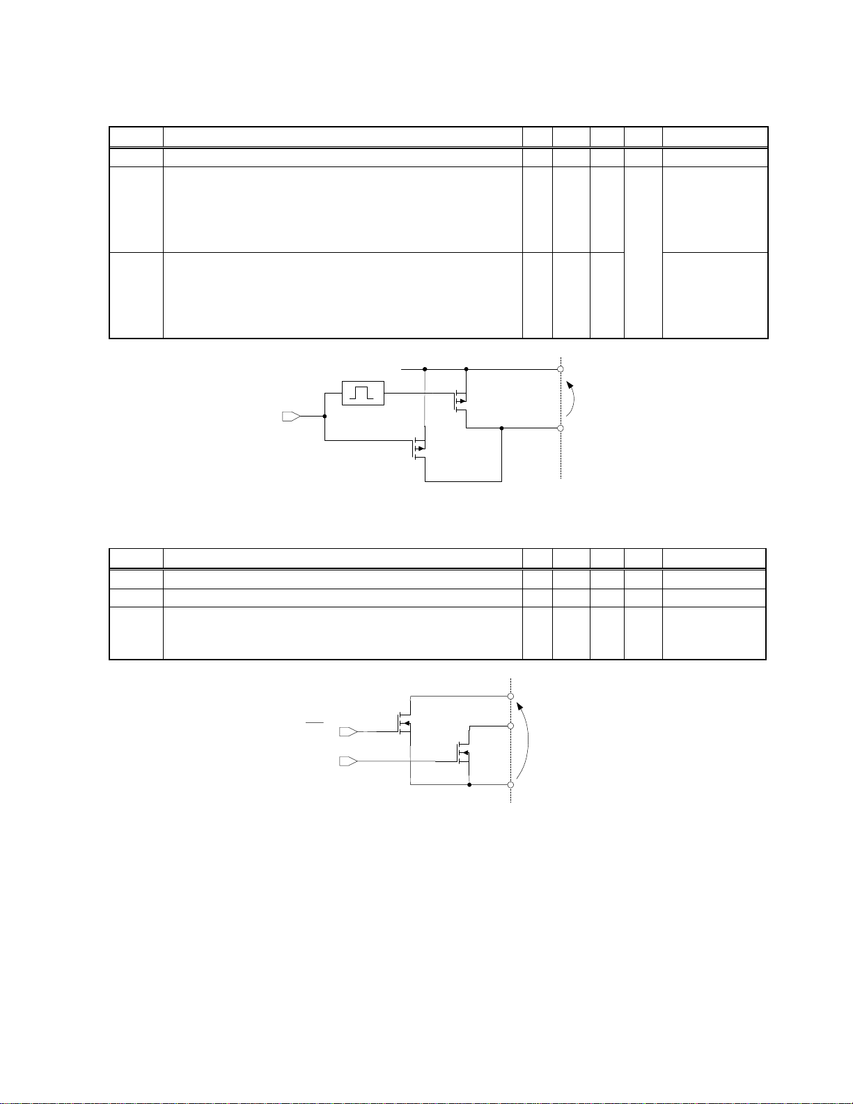
Pin: DSL, DSH
The active bias is present only in IR21141 and IR22141. V
COM and V
Symbol Definition Min Typ Max Units Test Conditions
VDESAT+ High desat input threshold voltage 7.2 8.0 8.8
VDESAT- Low desat input threshold voltage 6.3 7.0 7.7
VDSTH Desat input voltage hysteresis - 1.0 -
IDS+ High DSH or DSL input bias current - 21 - VDESAT = VCC or VBS
IDS- Low DSH or DSL input bias current - -160 -
IDSB DSH or DSL input bias current - -20 - mA VDESAT =
(IR21141 and IR22141 only) (VCC or VBS) - 2V
respectively for DSL and DSH.
S
DESAT
, IDS and I
parameters are referenced to
DSB
V See Fig. 16, 4
µA
VDESAT = 0V
VCC/VBS
DSL/DSH
DESAT
V
COM/VS
active
100k
bias
comparator
700k
Figure 4: DSH and DSL diagram.
SSD
internal
signal
4
Page 5
IR2114/IR21141/IR2214/IR22141
Pin: HOP, LOP
Symbol Definition Min Typ Max Units Test Conditions
VOH High level output voltage, VB – VHOP or Vcc –VLOP - 40 300
mV I
IO1+ Output high first stage short circuit pulsed current - 2 - VHOP/LOP=0V,
IO2+ Output high second stage short circuit pulsed current
- 1 -
A
200ns
oneshot
VCC/VB
O = 20mA
H
or LIN= 1,
IN
PW200ns,
resistive load,
see Fig. 8
VHOP/LOP=0V,
H
or LIN = 1,
IN
400nsPW10µs,
resistive load,
see Fig. 8
on/off
internal signal
VOH
LOP/HOP
Figure 5: HOP and LOP diagram
Pin: HON, LON, SSDH, SSDL
Symbol Definition Min Typ Max Units Test Conditions
VOL Low level output voltage, VHON or VLON - 45 300
RON,SSD Soft Shutdown on resistance (Note 1) - 90 -
IO- Output low short circuit pulsed current - 3 - A VHOP/LOP=15V,
mV I
O = 20mA
PW 7 µs
H
or LIN = 0,
IN
PW10µs
Note 1: SSD operation only.
LON/HON
on/off
internal signal
desat
internal signal
RON,SSD
SSDL/SSDH
VOL
COM/VS
Figure 6: HON, LON, SSDH and SSDL diagram
5
Page 6
IR2114/IR21141/IR2214/IR22141
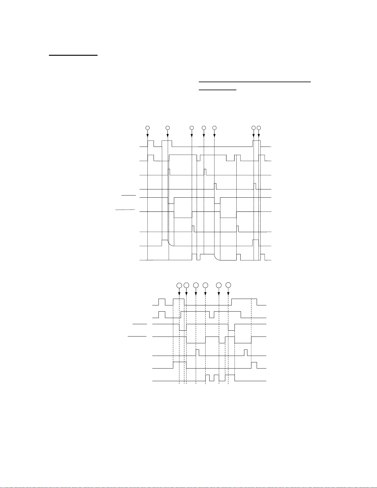
AC Electrical Characteristics
VCC = VBS = 15V, VS = VSS and TA = 25°C unless otherwise specified.
Symbol Definition Min. Typ. Max. Units Test Conditions
ton Turn on propagation delay 220 440 660 VIN = 0 & 1
toff Turn off propagation delay 220 440 660 VS = 0 to 600V or
1200V
tr Turn on rise time (C
tf Turn off fall time (C
ton1 Turn on first stage duration time 120 200 280 Figure 8
tDESAT1 DSH to HO soft shutdown propagation delay at HO 2000 3300 4600
turn on VHIN= 1
tDESAT2 DSH to HO soft shutdown propagation delay after 1050 — — VDESAT = 15V,Fig.10
Blanking
tDESAT3 DSL to LO soft shutdown propagation delay at LO 2000 3300 4600
turn on VLIN = 1
tDESAT4 DSL to LO soft shutdown propagation delay after 1050 — — VDESAT = 15V,Fig.10
Blanking
tDS Soft shutdown minimum pulse width of desat 1000 — — Figure 9
tSS Soft shutdown duration period 5000 9250 13500
VDS=15V,Fig. 9
=1nF) — 24 — HOP shorted to HON,
LOAD
=1nF) — 7 — Figure 7
LOAD
LOP shorted to LON,
ns
tSY_FLT, DSH to SY_FLT propagation delay at HO turn on — 3600 —
DESAT1
tSY_FLT, DSH to SY_FLT propagation delay after blanking 1300 — — VDS = 15V, Fig. 10
DESAT2
tSY_FLT, DSL to SY_FLT propagation delay at LO turn on — 3050 —
DESAT3
tSY_FLT, DSL to SY_FLT propagation delay after blanking 1050 — — VDESAT=15V,Fig.10
DESAT4
tBL DS blanking time at turn on — 3000 — VHIN = VLIN = 1
VDESAT=15V,Fig.10
Dead-time/Delay Matching Characteristics
DT Dead-time — 330 — Figure 11
MDT Dead-time matching, MDT=DTH-DTL — — 75 External DT=0nsec
Figure 11
PDM Propagation delay matching, — — 75 External DT>
Max(ton, toff) - Min(ton, toff)
VHIN = 1
VLIN = 1
500nsec, Fig.7
6
Page 7
HIN
LIN
IR2114/IR21141/IR2214/IR22141
3.3V
t
on
50%
t
r
PW
in
PW
out
50%
t
off
t
f
HO (HOP=HON)
LO (LOP=LON)
90%
90%
10%
10%
Figure 7: Switching Time Waveforms
Ton1
Io1+
Io2+
Figure 8: Output Source Current
3.3V
HIN/LIN
t
DS
DSH/DSL
SSD Driver Enable
8V
t
DESAT
8V
t
SS
HO/LO
Figure 9: Soft Shutdown Timing Waveform
7
Page 8

IR2114/IR21141/IR2214/IR22141
(
(
HIN
50%
50%
LIN
DSH
DSL
SY_FLT
FAULT/SD
FLTCLR
10%
HON
LON
8V
50%
LIN
HIN
50%
SY_FLT,DESAT1
t
tDESAT1
90%
tBL
Turn-On Propaga tion Delay
8V
50%
tSY_FLT,DESAT2
tDESAT2
90%
SoftShutdown
50%
tBL
SoftShutdown
Figure 10: Desat Timing
50% 50%
10%
50%
8V
50%
SY_FLT,DESAT3
t
t
DESAT3
tBL
Turn-On Propaga tion Delay
50%
90%
SoftShutdown
tSY_FLT,DESAT4
50%
8V
50%
Turn_Off propaga tion Delay
90%
t
DESAT4
90%
SoftShutdown
tBL
90%
HOP=HON)
HO
LOP=LON)
LO
50%
DTH
50%
50%
DTL
50%
MDT=DTH-DTL
Figure 11: Internal Dead-Time Timing
8
Page 9

IR2114/IR21141/IR2214/IR22141
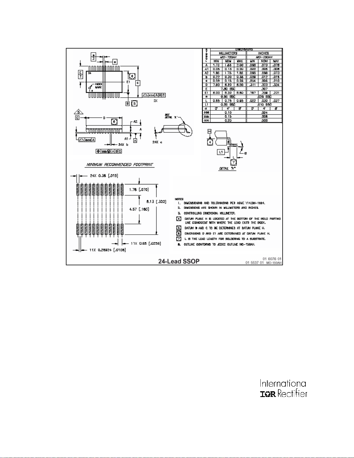
Lead Assignments
HIN
LIN
FLT_CLR
SY_FLT
24-Lead SSOP
Lead Definitions
Symbol Description
FAULT/SD
VSS
SSDL
COM
LON
LOP
VCC
DSL
1
SSOP24
12
24
13
DSH
VB
N.C.
HOP
HON
VS
SSDH
N.C.
N.C.
N.C.
N.C.
N.C.
VCC Low side gate driver supply
VSS Logic Ground
HIN Logic input for high side gate driver outputs (HOP/HON)
LIN Logic input for low side gate driver outputs (LOP/LON)
FAULT/SD
SY_FLT
FLT_CLR Fault clear active high input. Clears latched fault condition (See figure 17)
LOP Low side driver sourcing output
LON Low side driver sinking output
DSL Low side IGBT desaturation protection input
SSDL Low side soft shutdown
COM Low side driver return
VB High side gate driver floating supply
HOP High side driver sourcing output
HON High side driver sinking output
DSH High side IGBT desaturation protection input
SSDH High side soft shutdown
VS High side floating supply return
Dual function (in/out) active low pin. Refer to figures 17, 18 and 15. As an output, indicates fault
condition. As an input, shuts down the outputs of the gate driver regardless H
Dual function (in/out) active low pin. Refer to figures 17, 18 and 15. As an output, indicates SSD
sequence is occurring. As an input, an active low signal freezes both output status.
IN/LIN
status.
9
Page 10
Functional Block Diagram
IR2114/IR21141/IR2214/IR22141
VCC
HIN
LIN
UV_VCC
DETECT
SY_FLT
FAULT/SD
FAULT
FLT_CLR
VSS
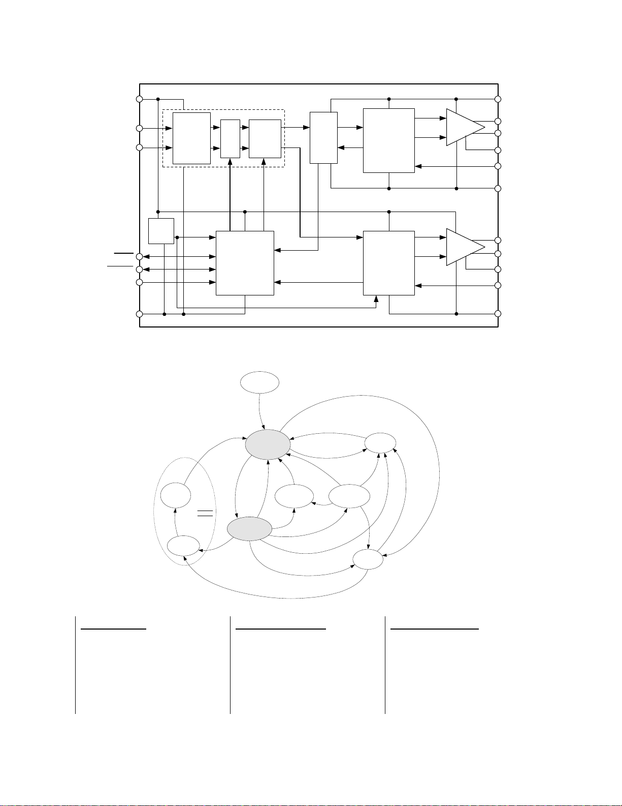
State Diagram
SCHMITT
TRIGGER
INPUT
SHOOT
THROUGH
PREVENTION
(DT) Deadtime
UV_VCC
HOLDSSD
SD
INPUT
HOLD
LOGIC
internal Hold
FAULT LOGIC
managemend
(See figure 14)
Start-Up
Sequence
OUTPUT
SHUTDOWN
LOGIC
Hard ShutDown
on/off (HS)
on/off (LS)
DesatHS
DesatLS
LEVEL
SHIFTERS
on/off
desat
LATCH
LOCAL DESAT
PROTECTION
SOFT SHUTDOW N
UV_VBS DETECT
LOCAL DESAT
PROTECTION
SOFTSHUTDOW N
on/off
soft
shutdown
on/off
soft
shutdown
di/dt control
Driver
di/dt control
Driver
VB
HOP
HON
SSDH
DSH
VS
LOP
LON
SSDL
DSL
COM
T
L
F
_
Y
FAULT
ShutDown
S
HO=LO=0
N
I
L
/
N
R
L
C
_
T
L
F
DESAT
EVENT
Soft
I
H
L
/
N
I
H
HO/LO=1
L
S
/
H
Y
S
_
D
F
L
T
N
I
F
A
_
V
U
UV_VBS
U
L
T
/
S
F
A
U
C
C
V
_
V
U
UnderVoltage
V
CC
HO=LO=0
C
C
V
D
L
T
/
S
D
UV_VCC
F
A
U
V
_
V
B
S
UnderVoltage
V
BS
HO=0, LO=LIN
U
L
T
/
S
D
ShutDown
D
S
/
T
L
U
A
F
S
Y
_
F
L
T
D
S
/
T
L
U
A
F
Freeze
L
/
H
S
D
Stable State
− FAULT
− HO=LO=0 (Normal operation)
− HO/LO=1 (Normal operation)
− UNDERVOLTAGE V
− SHUTDOWN (SD)
− UNDERVOLTAGE V
− FREEZE
CC
BS
Temporary State
− SOFT SHUTDOWN
− START UP SEQUENCE
System Variable
− FLT_CLR
− HIN/LIN
− UV_VCC
− UV_VBS
− DSH/L
− SY_FLT
− FAULT/SD
NOTE1: a change of logic value of the signal labeled on lines (system variable) generates a state transition.
NOTE2: Exiting from UNDERVOLTAGE V
.
H
IN
state, the HO goes high only if a rising edge event happens in
BS
10
Page 11
IR2114/IR21141/IR2214/IR22141
Logic Table
Output drivers status description
HO/LO
status
0 HiZ 0 HiZ
1 1 HiZ HiZ
SSD HiZ HiZ 0
LO/HO
LO
/HO
n-1
Operation
Shut Down
Fault Clear
Normal
Operation
Anti Shoot
Through
Soft Shut
Down
(entering)
Soft Shut
Down
(finishing)
Freeze
Under
Voltage
NOTE1: SY_FLT automatically resets after SSD event is over and FLT_CLR is not required. In order to avoid
FLT_CLR to conflict with the SSD procedure, FLT_CLR should not be operated while SY_FLT is active.
HOP/LOP HON/LON SSDH/SSDL
Output follows inputs (in=1->out=1, in=0->out=0)
n-1
Output keeps previous status
INPUTS
Lin
FLT_CLR
Hin
INPUT/OUTPUT
SY_FLT
SSD: desat (out)
HOLD: freezing (in)
FAULT/SD
SD: shutdown (in)
FAULT: diagnostic (out)
Under Voltage
Yes: V< UV threshold
No : V> UV threshold
X : don’t care
V
VBS HO LO
CC
OUTPUTS
X X X X 0 (SD) X X 0 0
(FAULT)
H
LIN
IN
NOTE1
No No HO
LO
1 0 0 1 1 No No 1 0
0 1 0 1 1 No No 0 1
0 0 0 1 1 No No 0 0
1 1 0 1 1 No No 0 0
1 0 0
0 1 0
X X 0
X X 0
(SSD)
(SSD)
(SSD) (FAULT)
(SSD) (FAULT)
X X X 0 (HOLD) 1 No No HO
X L
X 1 1 No Yes 0 LO
IN
1 No No SSD 0
1 No No 0 SSD
No No 0 0
No No 0 0
LO
n-1
X X X 1 0 (FAULT) Yes X 0 0
n-1
11
Page 12

IR2114/IR21141/IR2214/IR22141
FEATURES DESCRIPTION
1 Start-up sequence
At power supply start-up it is recommended to
keep FLT_CLR pin active until supply voltages are
properly established. This prevents spurious
diagnostic signals being generated. All protection
functions are operating independently from
FLT_CLR status and output driver status reflects
the input commands.
When bootstrap supply topology is used for
supplying the floating high side stage, the following
start-up sequence is recommended (see also
figure 12):
1. Set Vcc
2. Set FLT_CLR pin to HIGH level
3. Set LIN pin to HIGH level and let the
bootstrap capacitor be charged
4. Release LIN pin to LOW level
5. Release FLT_CLR pin to LOW level
VCC
FLT_CLR
LIN
LO
Figure 12 Start-up sequence
A minimum 15 us LIN and FLT-CLR pulse is
required.
2 Normal operation mode
After start-up sequence has been terminated, the
device becomes fully operative (see grey blocks in
the State Diagram).
HIN and LIN produce driver outputs to switch
accordingly, while the input logic checks the input
signals preventing shoot-through events and
including DeadTime (DT).
3 Shut down
The system controller can asynchronously
command the Hard ShutDown (HSD) through the
3.3 V compatible CMOS I/O FAULT/SD pin. This
event is not latched.
In a multi-phase system, FAULT/SD signals are orwired so the controller or one of the gate drivers
can force simultaneous shutdown to the other gate
drivers through the same pin.
4 Fault management
IR2114/21141/2214/22141 is able to manage the
both the supply failure (undervoltage lock out on
both low and high side circuits) and the
desaturation of both power transistors.
4.1 Undervoltage (UV)
The Undervoltage protection function disables the
driver’s output stage preventing the power device
being driven with too low voltages.
Both the low side (V
side (V
supplied) are controlled by a dedicate
BS
supplied) and the floating
CC
undervoltage function.
Undervoltage event on the V
V
< UV
CC
) generates a diagnostic signal by
VCC-
(when
CC
forcing FAULT/SD pin low (see FAULT/SD section
and figure 14). This event disables both low side
and floating drivers and the diagnostic signal holds
until the under voltage condition is over. Fault
condition is not latched and the FAULT/SD pin is
released once V
The undervoltage on the V
the floating driver. Undervoltage on V
becomes higher than UV
CC
works disabling only
BS
VCC+
does not
BS
.
prevent the low side driver to activate its output nor
generate diagnostic signals. V
condition (V
< UV
BS
) latches the high side
VBS-
output stage in the low state. V
reestablished higher than UV
undervoltage
BS
must be
BS
to return in
VBS+
normal operating mode. To turn on the floating
driver H
event on H
must be re-asserted high (rising edge
IN
is required).
IN
4.2 Power devices desaturation
Different causes can generate a power inverter
failure: phase and/or rail supply short-circuit,
overload conditions induced by the load, etc… In
all these fault conditions a large current increase is
produced in the IGBT.
The IR2114/21141/2214/22141 fault detection
circuit monitors the IGBT emitter to collector
voltage (V
diode. High current in the IGBT may cause the
transistor to desaturate, i.e. V
Once in desaturation, the current in power
transistor can be as high as 10 times the nominal
current. Whenever the transistor is switched off,
this high current generates relevant voltage
transients in the power stage that need to be
smoothed out in order to avoid destruction (by
over-voltages). The gate driver accomplishes the
transients control by smoothly turning off the
desaturated transistor by means of the SSD pin
activating a so called Soft ShutDown sequence
(SSD).
4.2.1 Desaturation detection: DSH/L function
Figure 13 shows the structure of the desaturation
sensing and soft shutdown block. This
configuration is the same for both high and low
side output stages.
) by means of an external high voltage
CE
to increase.
CE
12
Page 13

IR2114/IR21141/IR2214/IR22141
on/off
DesatHS/LS
SY_FLT
(external
hold)
tss
One Shot
VB/Vcc
PPrreeDDrriivveer
tBL
Blanking
r
ONE
SHOT
(ton1)
HOPH/L
HONH/L
SSDH/L
Ron,ss
RDSH/L
DSH/L
filter
tDS
desat
comparator
VDESAT
VS/COM
Figure 13: high and low side output stage
internal
HOLD
internal FAULT
(hard shutdown)
sensing
diode
FAULT/SD
(external hard
shutdown)
FLTCLR
Figure 14: fault management diagram
The external sensing diode should have BV>600V
or 1200V and low stray capacitance (in order to
minimize noise coupling and switching delays).
The diode is biased by an internal pull-up resistor
(equal to VCC/I
R
DSH/L
or VBS/I
DS-
for IR2114 or
DS-
IR2214) or by a dedicated circuit (see the activebias section for IR21141 and IR22141). When V
CE
increases, the voltage at DSH/L pin increases too.
Being internally biased to the local supply, DSH/L
voltage is automatically clamped. When DSH/L
exceeds the V
threshold the comparator
DESAT+
triggers (see figure 13). Comparator output is
filtered in order to avoid false desaturation
detection by externally induced noise; pulses
shorter than t
are filtered out. To avoid detecting
DS
a false desaturation during IGBT turn on, the
desaturation circuit is disabled by a Blanking signal
(T
, see Blanking block in figure 13). This time is
BL
the estimated maximum IGBT turn on time and
must be not exceeded by proper gate resistance
sizing. When the IGBT is not completely saturated
SET
S
Q
R
Q
CLR
DesatHS
DesatLS
UVCC
after T
, desaturation is detected and the driver
BL
will turn off.
Eligible desaturation signals initiate the Soft
Shutdown sequence (SSD). While in SSD, the
output driver goes in high impedance and the SSD
pull-down is activated to turn off the IGBT through
SSDH/L pin. The SY_FLT output pin (active low,
see figure 14) reports the gate driver status all the
way long SSD sequence lasts (t
). Once finished
SS
SSD, SYS_FLT releases, and the gate driver
generates a FAULT signal (see the FAULT/SD
section) by activating FAULT/SD pin. This
generates a hard shut down for both high and low
output stages (HO=LO=low). Each driver is latched
low until the fault is cleared (see FLT_CLR).
Figure 14 shows the fault management circuit. In
this diagram DesatHS and DesatLS are two
internal signals that come from the output stages
(see figure 13).
It must be noted that while in Soft Shut Down, both
Under Voltage fault and external Shut Down (SD)
13
Page 14

IR2114/IR21141/IR2214/IR22141
are masked until the end of SSD. Desaturation
protection is working independently by the other
entire control pin and it is disabled only when the
output status is off.
FAULT
SY_FLT
FAULT/SD
VCC
LIN
HIN
FLT_CLR
VB
HOP
HON
SSH
DSH
VS
LOP
IR2214
LON
SSL
DSL
COMVSS
phase U phase V phase W
SY_FLT
FAULT/SD
VCC
LIN
HIN
FLT_CLR
IR2214
VB
HOP
HON
SSH
DSH
VS
LOP
LON
SSL
DSL
COMVSS
SY_FLT
FAULT/SD
VCC
LIN
HIN
FLT_CLR
IR2214
VB
HOP
HON
SSH
DSH
VS
LOP
LON
SSL
DSL
COMVSS
Figure 15: IR2x14x application in 3ph system.
4.2.2 Fault management in multi-phase
systems
In a system with two or more gate drivers the
devices must be connected as in figure 15.
SY_FLT.
The bi-directional SY_FLT pins communicate each
other in the local network. The logic signal is active
low.
The device that detects the IGBT desaturation
activates the SY_FLT, which is then read by the
other gate drivers. When SYS_FLT is active all the
drivers hold their output state regardless the input
signals (H
, LIN) they receive from the controller
IN
(freeze state).
This feature is particularly important in phase-tophase short circuit where two IGBTs are involved;
in fact, while one is softly shutting-down, the other
must be prevented from hard shutdown to avoid
vanishing SSD.
In the Freeze state the frozen drivers are not
completely inactive because desaturation detection
still takes the highest priority.
SY_FLT communication has been designed for
creating a local network between the drivers. There
is no need to wire SY_FLT to the controller.
FAULT/SD
The bi-directional FAULT/SD pins communicates
each other and with the system controller. The
logic signal is active low.
When low, the FAULT/SD signal commands the
outputs to go off by hard shutdown. There are
three events that can force FAULT/SD low:
1. Desaturation detection event: the
FAULT\SD pin is latched low when SSD is
over, and only a FLT_CLR signal can reset
it.
2. Undervoltage on V
: the FAULT\SD pin is
CC
forced low and held until the undervoltage
is active (not latched).
3. FAULT/SD is externally driven low either
from the controller or from another
IR2x14x device. This event is not latched;
therefore the FLT_CLR cannot disable it.
Only when FAULT/SD becomes high the
device returns in normal operating mode.
5 Active bias
For the purpose of sensing the power transistor
desaturation the collector voltage is read by an
external HV diode. The diode is normally biased by
an internal pull up resistor connected to the local
supply line (V
the diode is conducting and the amount of current
flowing in the circuit is determined by the internal
pull up resistor value.
In the high side circuit, the desaturation biasing
current may become relevant for dimensioning the
bootstrap capacitor (see figure 19). In fact, too low
pull up resistor value may result in high current
discharging significantly the bootstrap capacitor.
For that reason typical pull up resistor are in the
range of 100 k. This is the value of the internal
pull up.
While the impedance of DSH/DSL pins is very low
when the transistor is on (low impedance path
through the external diode down to the power
transistor), the impedance is only controlled by the
pull up resistor when the transistor is off. In that
case relevant dV/dt applied by the power transistor
during the commutation at the output results in a
considerable current injected through the stray
capacitance of the diode into the desaturation
detection pin (DSH/L). This coupled noise may be
easily reduced using an active bias for the sensing
diode.
An Active Bias structure is available only for
IR21141 or IR22141 version for DSH/L pin. The
DSH/L pins present an active pull-up respectively
to VB/VCC, and a pull-down respectively to
VS/COM.
The dedicated biasing circuit reduces the
impedance on the DSH/L pin when the voltage
exceeds the V
low impedance helps in rejecting the noise
providing the current inject by the parasitic
capacitance. When the power transistor is fully on,
the sensing diode gets forward biased and the
voltage at the DSH/L pin decreases. At this point
the biasing circuit deactivates, in order to reduce
the bias current of the diode as shown in figure 16.
or VCC). When the transistor is “on”
B
threshold (see figure 16). This
DESAT
DSH/L
R
100K ohm
100 ohm
VDSH/L
Figure 16: R
-
+
T
T
A
A
S
S
E
E
D
D
V
V
Active Biasing
DSH/L
14
Page 15
IR2114/IR21141/IR2214/IR22141
6 Output stage
The structure is shown in figure 13 and consists of
two turns on stages and one turn off stage.
When the driver turns on the IGBT (see figure 8), a
first stage is constantly activated while an
additional stage is maintained active only for a
limited time (ton1). This feature boost the total
driving capability in order to accommodate both
fast gate charge to the plateau voltage and dV/dt
control in switching.
A B C D E F G
HIN
LIN
DSH
DSL
SY_FLT
FAULT/SD
At turn off, a single n-channel sinks up to 3A (I
and offers a low impedance path to prevent the
self-turn on due to the parasitic Miller capacitance
in the power switch.
7 Timing and logic state diagrams
description
The following figures show the input/output logic
diagram.
Figure 17 shows the SY_FLT and FAULT/SD
signals as output, whereas figure 18 as input.
)
O-
FLT_CLR
HO(HOP/HON)
LO(LOP/LON)
Figure 17: I/O timing diagram with SY_FLT and FAULT/SD as output
HIN
LIN
SY_FLT
FAULT/SD
FLT_CLR
HO (HOP/HON)
LO (LOP/LON)
Figure 18: I/O logic diagram with SY_FLT and FAULT/SD as input
Referred to timing diagram of figure 17:
A. When the input signals are on together
the outputs go off (anti-shoot through).
B. The HO signal is on and the high side
IGBT desaturates, the HO turn off softly
while the SY_FLT stays low. When
ABCD EF
SY_FLT goes high the FAULT/SD goes
low. While in SSD, if LIN goes up, LO
does not change (freeze).
C. When FAULT/SD is latched low (see
FAULT/SD section) FLT_CLR can disable
15
Page 16
IR2114/IR21141/IR2214/IR22141
−≤∆
++=
it and the outputs go back to follow the
inputs.
D. The DSH goes high but this is not read
because HO is off.
E. The LO signal is on and the low side
IGBT desaturates, the low side behaviour
is the same as described in point B.
F. The DSL goes high but this is not read
because LO is off.
G. As point A (anti-shoot through).
Referred to timing diagram figure 18:
A. The device is in hold state, regardless of
input variations. Hold state is forced by
SY_FLT forced low externally
B. The device outputs goes off by hard
shutdown, externally commanded. A
through B is the same sequence adopted
by another IR2x14x device in SSD
procedure.
C. Externally driven low FAULT/SD
(shutdown state) cannot be disabled by
forcing FLT_CLR (see FAULT/SD
section).
D. The FAULT/SD is released and the
outputs go back to follow the inputs.
E. Externally driven low FAULT/SD: outputs
go off by hard shutdown (like point B).
F. As point A and B but for the low side
output.
Sizing tips
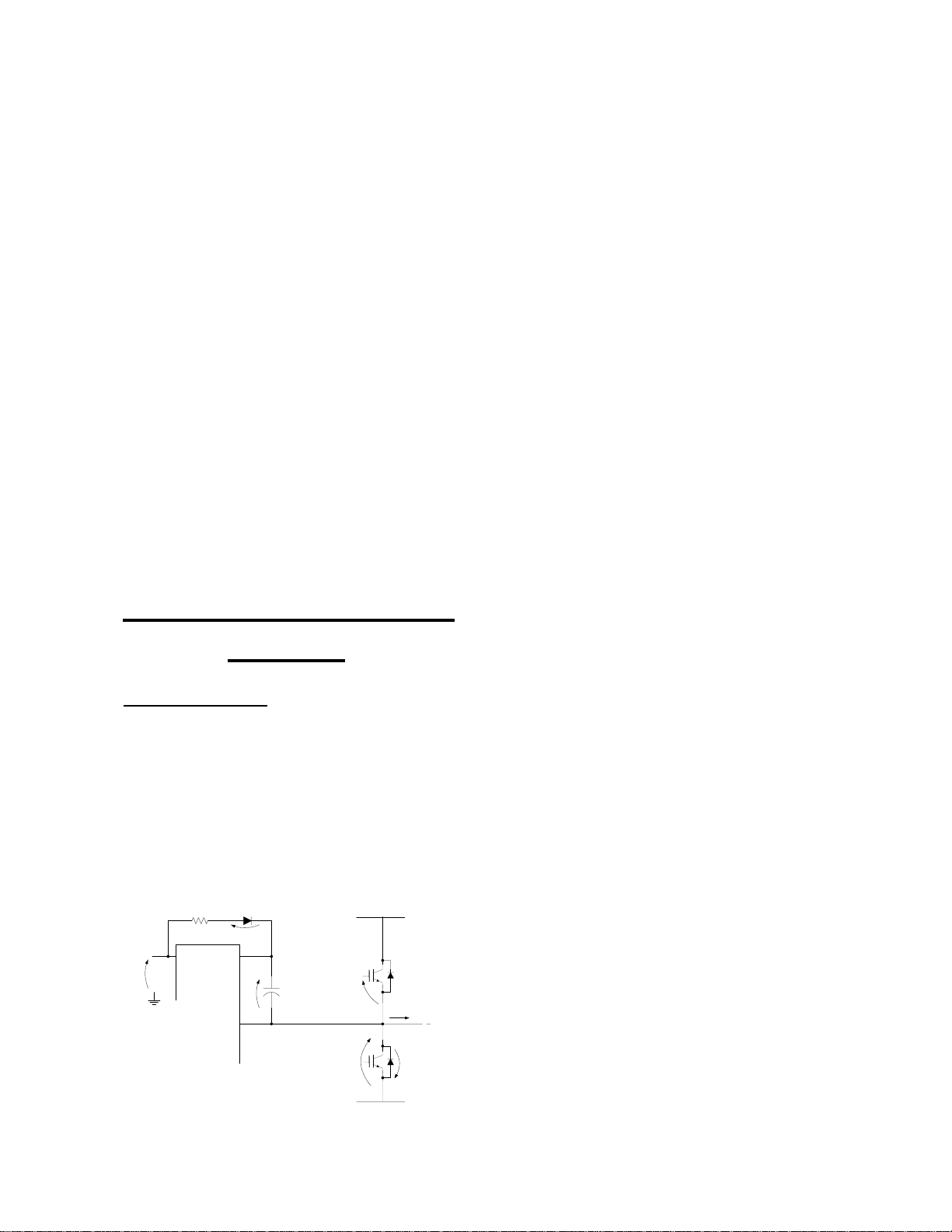
Bootstrap supply
The V
side driver circuitry of the gate driver. This supply
sits on top of the V
floating.
The bootstrap method to generate V
be used with any of the IR2114, IR21141,
IR2214, IR22141. The bootstrap supply is formed
by a diode and a capacitor connected as in figure
19.
VCC
voltage provides the supply to the high
BS
voltage and so it must be
S
resistor
R
bootstrap
diode
boot
VF
VB
HOP
HON
VS
IR2214
SSDH
bootstrap
VBS
capacitor
bootstrap
VCC
Figure 19: bootstrap supply schematic
supply can
BS
DC+
VGE
VCEon
COM
ILOAD
motor
VFP
This method has the advantage of being simple
and low cost but may force some limitations on
duty-cycle and on-time since they are limited by
the requirement to refresh the charge in the
bootstrap capacitor.
Proper capacitor choice can reduce drastically
these limitations.
Bootstrap capacitor sizing
To size the bootstrap capacitor, the first step is to
establish the minimum voltage drop (∆V
we have to guarantee when the high side IGBT is
on.
If V
is the minimum gate emitter voltage we
GEmin
want to maintain, the voltage drop must be:
VVVVV −−
min
under the condition:
>
−
BSUVGEVVmin
where V
diode forward voltage, V
voltage of low side IGBT and V
is the IC voltage supply, VF is bootstrap
CC
is emitter-collector
CEon
BSUV-
side supply undervoltage negative going
threshold.
Now we must consider the influencing factors
contributing V
to decrease:
BS
− IGBT turn on required Gate charge (Q
− IGBT gate-source leakage current (I
− Floating section quiescent current (I
− Floating section leakage current (I
− Bootstrap diode leakage current (I
− Desat diode bias when on (I
DS-
)
− Charge required by the internal level shifters
(Q
); typical 20nC
LS
− Bootstrap capacitor leakage current
(I
);
LK_CAP
− High side on time (T
I
is only relevant when using an electrolytic
LK_CAP
HON
).
capacitor and can be ignored if other types of
capacitors are used. It is strongly recommend
using at least one low ESR ceramic capacitor
(paralleling electrolytic and low ESR ceramic may
result in an efficient solution).
Then we have:
++
(
The minimum size of bootstrap capacitor is:
IIQQQ
QBSGELKLSGTOT
_
__
) that
BS
CEonGEFCCBS
is the high-
);
G
);
LK_GE
);
QBS
)
LK
LK_DIODE
);
TIIII ⋅++++
)
HONDSCAPLKDIODELKLK
−
16
Page 17

IR2114/IR21141/IR2214/IR22141
=
=
−
=
Q
TOT
C
BOOT
min
=
V
∆
BS
An example follows using IR2214SS or
IR22141SS:
a) using a 25A @ 125C 1200V IGBT
(IRGP30B120KD):
• I
= 800 µA (This Datasheet);
QBS
= 50 µA (See Static Electrical Charact.);
• I
LK
= 20 nC;
• Q
LS
= 160 nC (Datasheet IRGP30B120KD);
• Q
G
• I
• I
= 100 nA (Datasheet IRGP30B120KD);
LK_GE
= 100 µA (with reverse recovery time
LK_DIODE
<100 ns);
• I
• I
• T
= 0 (neglected for ceramic capacitor);
LK_CAP
= 150 µA (see Static Electrical Charact.);
DS-
= 100 µs.
HON
And:
• V
• V
• V
• V
= 15 V
CC
= 1 V
F
CEonmax
= 10.5 V
GEmin
= 3.1 V
the maximum voltage drop ∆V
becomes
BS
min
VVVVV
CEonGEFCCBS
−−−=
VVVVV 4.01.35.10115
=−−−≤∆
And the bootstrap capacitor is:
C
BOOT
290
V
4.0
=≥
725
nF
nC
NOTICE: Here above V
has been chosen
CC
to be 15V. Some IGBTs may require higher
supply to work correctly with the bootstrap
technique. Also Vcc variations must be
accounted in the above formulas.
Some important considerations
a. Voltage ripple
There are three different cases making the
bootstrap circuit gets conductive (see figure 19)
I
< 0; the load current flows in the low
LOAD
side IGBT displaying relevant V
In this case we have the lowest value for V
This represents the worst case for the bootstrap
capacitor sizing. When the IGBT is turned off
CEon
VVVV −−=
CEonFCCBS
.
BS
the Vs node is pushed up by the load current
until the high side freewheeling diode get
forwarded biased
I
on and V
= 0; the IGBT is not loaded while being
LOAD
can be neglected
CE
VVV −
FCCBS
I
> 0; the load current flows through the
LOAD
freewheeling diode
VVVV +
FPFCCBS
In this case we have the highest value for V
Turning on the high side IGBT, I
and V
is pulled up.
S
flows into it
LOAD
BS
.
To minimize the risk of undervoltage, bootstrap
capacitor should be sized according to the I
LOAD
<0
case.
b. Bootstrap Resistor
A resistor (R
boot
) is placed in series with bootstrap
diode (see figure 19) so to limit the current when
the bootstrap capacitor is initially charged. We
suggest not exceeding some Ohms (typically 5,
maximum 10 Ohm) to avoid increasing the V
BS
time-constant. The minimum on time for charging
the bootstrap capacitor or for refreshing its charge
must be verified against this time-constant.
c. Bootstrap Capacitor
For high T
designs where is used an
HON
electrolytic tank capacitor, its ESR must be
considered. This parasitic resistance forms a
voltage divider with R
on V
at the first charge of bootstrap capacitor.
BS
The voltage step and the related speed (dV
generating a voltage step
boot
BS
/dt)
should be limited. As a general rule, ESR should
meet the following constraint:
ESR
+
RESR
BOOT
CC
VV
3≤⋅
Parallel combination of small ceramic and large
electrolytic capacitors is normally the best
compromise, the first acting as fast charge thank
for the gate charge only and limiting the dV
BS
/dt
by reducing the equivalent resistance while the
second keeps the V
desired ∆V
BS
.
voltage drop inside the
BS
d. Bootstrap Diode
The diode must have a BV> 600V or 1200V and a
fast recovery time (trr < 100 ns) to minimize the
amount of charge fed back from the bootstrap
capacitor to V
supply.
CC
17
Page 18

IR2114/IR21141/IR2214/IR22141
+
=
t
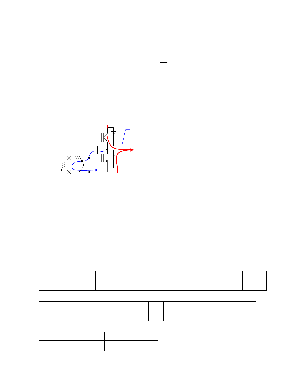
Gate resistances
The switching speed of the output transistor can
be controlled by properly size the resistors
controlling the turn-on and turn-off gate current.
The following section provides some basic rules
for sizing the resistors to obtain the desired
switching time and speed by introducing the
equivalent output resistance of the gate driver
(R
DRp
and R
DRn
).
The examples always use IGBT power transistor.
Figure 20 shows the nomenclature used in the
following paragraphs. In addition, V
the plateau voltage, Q
and Q
gc
ge
*
indicates
ge
indicate the gate
to collector and gate to emitter charge
respectively.
I
C
GC
VGE
I
C
C
C
t,Q
RESon
RESoff
Vge*
C
RES
VGE
t1,Q
GE
V
CE
90%
t2,Q
dV/dt
C
RES
10%
10%
t
SW
t
Don
t
R
Figure 20: Nomenclature
Sizing the turn-on gate resistor
-
Switching-time
For the matters of the calculation included
hereafter, the switching time t
time spent to reach the end of the plateau voltage
(a total Q
has been provided to the IGBT
gc+Qge
gate). To obtain the desired switching time the
gate resistance can be sized starting from Q
, Vcc, V
Q
gc
*
(see figure 21):
ge
QQI+
gegc
avg
=
t
sw
and
*
−
VVcc
ge
=
R
TOT
I
avg
is defined as the
sw
ge
and
I
Vcc/Vb
R
DRp
R
COM/Vs
Figure 21: R
where
= gate on-resistor
R
Gon
R
= driver equivalent on-resistance
DRp
When R
> 7 Ohm, R
Gon
Vcc
I
=
R
DRp
Vcc
I
oo
Vcc
I
++
o
+
1
(I
,I
O1+
and t
O2+
on1
Characteristics”).
Table 1 reports the gate resistance size for two
commonly used IGBTs (calculation made using
typical datasheet values and assuming Vcc=15V).
- Output voltage slope
Turn-on gate resistor R
output slope
While the output voltage has a non-linear
behaviour, the maximum output slope can be
approximated by:
dV
out
dt
inserting the expression yielding I
rearranging:
R
TOT
As an example, table 2 shows the sizing of gate
resistance to get dV
popular IGBTs, typical datasheet values and
assuming Vcc=15V.
(dV
I
avg
=
C
RESoff
=
C
RESoff
/dt).
OUT
*
−
VVcc
ge
dV
out
⋅
d
out
avg
C
RES
Gon
sizing
Gon
RRR
GonDRpTOT
is defined by
DRp
t
SW
−+
1
t
on
121
>
ttwhen
onSW
≤
ttwhen
onSW
from “static Electrical
can be sized to control
Gon
and
avg
/dt=5V/ns when using two
1
1
18
Page 19
IR2114/IR21141/IR2214/IR22141
(
NOTICE: Turn on time must be lower than TBL to
avoid improper desaturation detection and SSD
triggering.
Sizing the turn-off gate resistor
The worst case in sizing the turn-off resistor R
is when the collector of the IGBT in off state is
Goff
As a result, when τ is faster than the collector rise
time (to be verified after calculation) the transfer
function can be approximated by:
V
ge
V
de
forced to commutate by external events (i.e. the
turn-on of the companion IGBT).
In this case the dV/dt of the output node induces a
parasitic current through C
and R
(see figure 22).
DRn
flowing in R
RESoff
Goff
So that
time domain.
Then the condition:
If the voltage drop at the gate exceeds the
threshold voltage of the IGBT, the device may self
turn on causing large oscillation and relevant
cross conduction.
must be verified to avoid spurious turn on.
Rearranging the equation yields:
dV/dt
V
C
RESoff
th
⋅
R −
<
Goff
In any case, the worst condition for unwanted turn
on is with very fast steps on IGBT collector.
In that case collector to gate transfer function can
ON
HS Turning ON
R
Goff
R
DRn C
C
RESoff
OFF
IES
be approximated with the capacitor divider:
Figure 22: R
sizing: current path when Low
Goff
Side is off and High Side turns on
The transfer function between IGBT collector and
IGBT gate then becomes:
)(
V
ge
=
V
de
CRRs
⋅+⋅
RESoffDRnGoff
+⋅+⋅+
)()(1
CCRRs
IESRESoffDRnGoff
Which yields to a high pass filter with a pole at:
/1
=
τ
1
)()(
CCRR +⋅+
IESRESoffDRnGoff
VV
dege
which is driven only by IGBT characteristics.
As an example, table 3 reports R
with the above mentioned disequation) for two
popular IGBTs to withstand dV
NOTICE: the above-described equations are
intended being an approximated way for the gate
resistances sizing. More accurate sizing may
account more precise device modelling and
parasitic component dependent on the PCB and
power section layout and related connections.
C
⋅=
Table 1: tsw driven R
IGBT Qge Qgc Vge* tsw Iavg Rtot
IRGP30B120K(D) 19nC 82nC 9V 400ns 0.25A
IRG4PH30K(D) 10nC 20nC 9V 200ns 0.15A
Table 2: dV
IGBT Qge Qgc Vge* CRESoff Rtot
IRGP30B120K(D) 19nC 82nC 9V 85pF
IRG4PH30K(D) 10nc 20nC 9V 14pF
Table 3: R
IGBT Vth(min) CRESoff RGoff
IRGP30B120K(D) 4 85pF RGoff 4
IRG4PH30K(D) 3 14pF RGoff 35
/dt driven R
OUT
sizing
Goff
sizing
Gon
sizing
Gon
RGon
→ std commercial value
24
Ω RTOT - RDRp = 12.7 → 10 →420ns
40
Ω RTOT - RDRp = 32.5 → 33 →202ns
→ std commercial value
RGon
14
Ω RTOT - RDRp = 6.5 → 8.2 →4.5V/ns
85
Ω RTOT - RDRp = 78 → 82 →5V/ns
dV
dt
RESoff
CRRs
⋅+⋅= )(
)
R
DRn
CC
+
IESRESoff
RESoffDRnGoff
CRRV
CRRVV
⋅+=>
RESoffDRnGoffgeth
⋅⋅+= )( in the
RESoffDRnGoffge
dV
out
dt
dV
)(
(calculated
Goff
/dt = 5V/ns.
out
dVout/dt
de
dt
Tsw
19
Page 20

PCB LAYOUT TIPS
Distance from H to L voltage:
The IR2x14x pin out maximizes the distance
between floating (from DC- to DC+) and low
voltage pins. It’s strongly recommended to place
components tied to floating voltage in the high
voltage side of device (V
components in the opposite side.
Ground plane:
Ground plane must not be placed under or nearby
the high voltage floating side to minimize noise
coupling.
Gate drive loops:
Current loops behave like an antenna able to
receive and transmit EM noise. In order to reduce
EM coupling and improve the power switch turn
on/off performances, gate drive loops must be
reduced as much as possible. Figure 23 shows
the high and low side gate loops.
Moreover, current can be injected inside the gate
drive loop via the IGBT collector-to-gate parasitic
capacitance. The parasitic auto-inductance of the
gate loop contributes to develop a voltage across
the gate-emitter increasing the possibility of self
turn-on effect. For this reason is strongly
recommended to place the three gate resistances
close together and to minimize the loop area (see
figure 23).
VB/ VCC
H/LOP
H/LON
SSDH/L
gate
resistance
, VS side) while the other
B
IGC
CGC
Gate Drive
Loop
VGE
IR2114/IR21141/IR2214/IR22141
Routing and placement example:
Figure 24 shows one of the possible layout
solutions using a 3 layer PCB. This example takes
into account all the previous considerations.
Placement and routing for supply capacitors and
gate resistances in the high and low voltage side
minimize respectively supply path and gate drive
loop. The bootstrap diode is placed under the
device to have the cathode as close as possible to
bootstrap capacitor and the anode far from high
voltage and close to V
V
V
V
V
R2
GH
R3
R4
R5
GL
R6
R7
EH
V
CC
EL
.
CC
D2
DC+
IR2214
D3
Phase
C2
a)
C1
D1
R1
b)
VS/COM
Figure 23: gate drive loop
Supply capacitors:
IR2x14x output stages are able to quickly turn on
IGBT with up to 2 A of output current. The supply
capacitors must be placed as close as possible to
the device pins (V
supply, V
and VS for the floating supply) in order
B
to minimize parasitic inductance/resistance.
and VSS for the ground tied
CC
c)
Figure 24: layout example: top (a), bottom (b) and
ground plane (c) layer
Referred to figure 24:
Bootstrap section: R1, C1, D1
High side gate: R2, R3, R4
High side Desat: D2
Low side supply: C2
Low side gate: R5, R6, R7
Low side Desat: D3
20
Page 21
Case Outline
IR2114/IR21141/IR2214/IR22141
IR WORLD HEADQUARTERS:
233 Kansas St., El Segundo, California 90245 Tel: (310) 252-7105
This product has been designed and qualified for industrial market
Data and specifications subject to change without notice. 3/24/2005
21
 Loading...