

Page 1
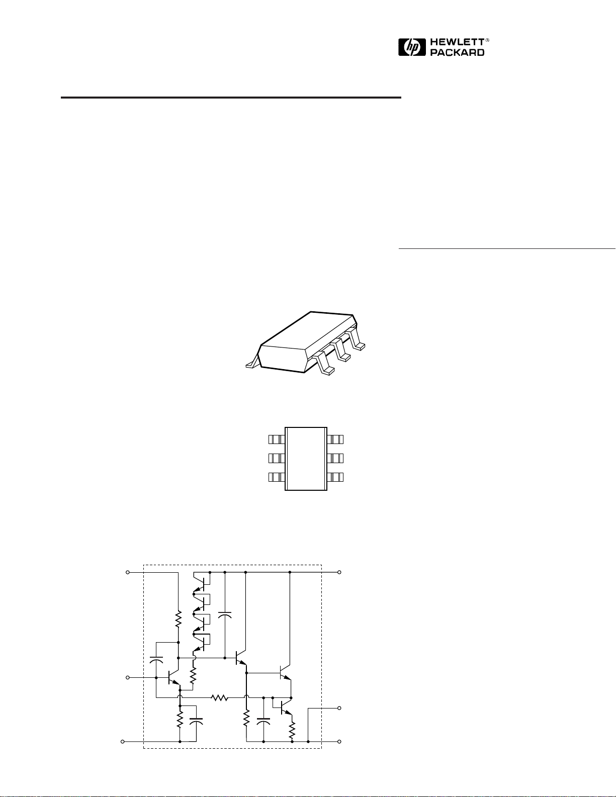
1.5 GHz Low Noise Silicon
MMIC Amplifier
Technical Data
INA-52063
Features
• Ultra-Miniature Package
• Single 5 V Supply (30 mA)
• 22 dB Gain
• 8 dBm P
1dB
• Unconditionally Stable
Applications
• Amplifier for Cellular,
Cordless, Special Mobile
Radio, PCS, ISM, Wireless
LAN, DBS, TVRO, and TV
Tuner Applications
Equivalent Circuit
(Simplified)
Surface Mount SOT-363 (SC-70) Package
Pin Connections and Package Marking
GND
2
GND
1
INPUT
3
Note: Package marking provides
orientation and identification.
52
OUTPUT
6
and V
GND 3
5
4V
CC
Description
Hewlett-Packard’s INA-52063 is a
Silicon monolithic amplifier that
offers excellent gain and power
output for applications to
1.5 GHz. Packaged in an ultraminiature SOT-363 package, it
requires half the board space of a
SOT-143 package.
The INA-52063 is fabricated using
HP’s 30 GHz f
MAX
ISOSAT
Silicon bipolar process which
CC
uses nitride self-alignment submicrometer lithography, trench
isolation, ion implantation, gold
metallization, and polyimide
intermetal dielectric and scratch
protection to achieve superior
performance, uniformity, and
reliability.
TM
GROUND 2
5965-9681E
V
CC
RF
INPUT
6-156
RF
OUTPUT
& V
CC
GROUND 1
GROUND 3
Page 2

Absolute Maximum Ratings
Absolute
Symbol Parameter Units Maximum
V
CC
P
in
T
j
T
STG
Supply Voltage, to Ground V 12
CW RF Input Power dBm +13
Junction Temperature ° C 150
Storage Temperature °C - 65 to 150
[1]
Thermal Resistance
θ
= 170°C/W
j-c
Notes:
1. Operation of this device above any one
of these limits may cause permanent
damage.
2. T
= 25°C (T
C
temperature at the package pins where
contact is made to the circuit board)
is defined to be the
C
[2]
:
INA-52063 Electrical Specifications, T
= 25°C, ZO = 50 Ω, V
C
= 5 V, unless noted
CC
Symbol Parameters and Test Conditions Units Min. Typ. Max.
G
p
Power Gain (|S21|2) f = 900 MHz dB 20 22
NF Noise Figure f = 900 MHz dB 4.0
P
1dB
IP
3
IP
3
Output Power at 1 dB Gain Compression f = 900 MHz dBm +8
Third Order Intercept Point f = 900 MHz dBm +20
Third Order Intercept Point f = 2100 MHz dBm +15
VSWR Input VSWR f = 900 MHz 1.4
Output VSWR f = 900 MHz 1.3
I
CC
ι
d
Device Current mA 30 38
Group Delay f = 900 MHz ps 238
6-157
Page 3

INA-52063 Typical Performance, T
= 25°C, ZO = 50 Ω, V
C
= 5 V, unless noted
CC
24.0
23.0
22.0
21.0
20.0
19.0
GAIN (dB)
18.0
17.0
16.0
15.0
0.05
0.65
1.25 1.85
FREQUENCY (GHz)
5.5 V
5.0 V
4.5 V
Figure 1. Gain vs. Frequency and
Voltage.
24.0
23.0
22.0
21.0
20.0
19.0
GAIN (dB)
18.0
17.0
16.0
15.0
0.05
0.60
1.20 1.80
FREQUENCY (GHz)
-40 °C
+25 °C
+85 °C
6.0
5.5 V
5.0 V
4.5 V
0.2
0.5 1.1 1.7
FREQUENCY (GHz)
2.45
5.5
5.0
4.5
NOISE FIGURE (dB)
4.0
3.5
0.09 2.6
Figure 2. Noise Figure vs. Frequency
and Voltage.
2.40
7.0
6.5
6.0
5.5
5.0
4.5
4.0
NOISE FIGURE (dB)
3.5
3.0
0.05
-40 °C
+25 °C
+85 °C
0.80
0.40
FREQUENCY (GHz)
1.20
1.60 2.00
12.0
11.0
10.0
9.0
8.0
7.0
6.0
P1dB (dBm)
5.0
4.0
3.0
2.0
2.30.8 1.4 2.0
0.05
5.5 V
5.0 V
4.5 V
0.30
FREQUENCY (GHz)
2.400.60 1.20 1.80
Figure 3. Output Power for 1 dB Gain
Compression vs. Frequency and
Voltage.
2.40
12
11
10
9
8
7
P1dB (dBm)
6
5
4
0.05
0.60
0.30
FREQUENCY (GHz)
1.20 1.80
-40 °C
+25 °C
+85 °C
2.40
Figure 4. Gain vs. Frequency and
Temperature.
2.2
2.0
1.8
1.6
VSWR (dB)
1.4
1.2
1.0
0.0
5
VSWR IN
VSWR OUT
0.7
0.4
0
1.1
5
0
FREQUENCY (GHz)
1.4
5
5
0
2.1
1.8
Figure 7. Input and Output VSWR vs.
Frequency.
Figure 5. Noise Figure vs. Frequency
and Temperature.
60
-40 °C
+25 °C
+85 °C
1.0 3.0 5.0
VCC (V)
2.5
50
40
30
(mA)
CC
I
20
10
0
0
0.0
Figure 8. Supply Current vs. Voltage
and Temperature.
6-158
Figure 6. Output Power for 1 dB Gain
Compression vs. Frequency and
Temperature.
7.02.0 4.0 6.0
Page 4
INA-52063 Typical Scattering Parameters
Freq. S
11
S
21
[3]
, T
= 25°C, ZO = 50 Ω, V
C
= 5.0 V
CC
S
12
S
22
GHz Mag Ang dB Mag Ang dB Mag Ang Mag Ang Factor
0.05 0.06 165 23.5 14.88 -5 -29.3 0.034 0 0.05 1 1.24
0.10 0.06 154 23.4 14.84 -9 -29.3 0.034 0 0.05 0 1.24
0.20 0.06 131 23.4 14.72 -19 -29.4 0.034 0 0.05 -1 1.25
0.30 0.07 104 23.3 14.57 -28 -29.5 0.034 1 0.06 -5 1.25
0.40 0.07 80 23.1 14.33 -37 -29.4 0.034 2 0.07 -10 1.26
0.50 0.09 66 23.0 14.08 -46 -29.4 0.034 3 0.08 -14 1.27
0.60 0.10 46 22.8 13.76 -55 -29.4 0.034 4 0.09 -21 1.28
0.70 0.12 30 22.6 13.41 -64 -29.3 0.034 5 0.11 -29 1.29
0.80 0.13 14 22.3 13.01 -73 -29.2 0.035 6 0.13 -37 1.28
0.90 0.15 0 22.0 12.59 -82 -29.0 0.036 6 0.14 -45 1.27
1.00 0.17 -12 21.7 12.14 -90 -28.8 0.036 7 0.16 -52 1.28
1.20 0.21 -33 21.0 11.22 -106 -28.4 0.038 7 0.20 -67 1.25
1.40 0.24 -50 20.2 10.28 -122 -28.1 0.040 6 0.23 -81 1.24
1.60 0.27 -66 19.4 9.38 -137 -27.7 0.041 4 0.25 -94 1.26
1.80 0.30 -80 18.6 8.55 -151 -27.5 0.042 2 0.27 -107 1.29
2.00 0.32 -93 17.8 7.80 -164 -27.4 0.043 -1 0.29 -118 1.33
2.20 0.33 -105 17.1 7.13 -177 -27.6 0.042 -5 0.30 -129 1.44
2.40 0.35 -117 16.3 6.52 170 -27.8 0.041 -8 0.31 -139 1.56
2.60 0.36 -128 15.5 5.98 159 -28.1 0.039 -12 0.32 -149 1.74
2.80 0.36 -139 14.8 5.52 147 -28.9 0.036 -15 0.33 -158 2.01
3.00 0.36 -149 14.1 5.08 136 -29.5 0.033 -16 0.33 -168 2.37
K
Note: 3. Reference plane per Figure 9 in Applications Information section.
INA-52063 Applications Information
Introduction
The INA-52063 is a silicon RFIC
amplifier that is designed with an
internal resistive feedback net-
work to provide a 50 Ω input and
50 Ω output impedance. With a
Third Order Intercept Point of
+20 dBm and a low Noise Figure
of 4 dB, the INA-52063 is
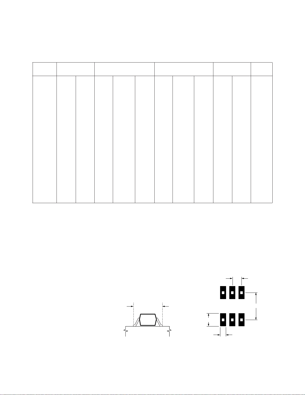
SOT-363 PCB Layout
The INA-52063 is packaged in the
miniature SOT-363 (SC-70)
surface mount package. A PCB
pad layout for the SOT-363
package is shown in Figure 10
(dimensions are in inches). This
layout provides ample allowance
for package placement by
automated assembly equipment
without adding pad parasitics that
especially useful for RF and IF
amplifier applications requiring
high dynamic ranges.
REFERENCE
PLANES
Phase Reference Planes
The positions of the reference
planes used to measure
TEST CIRCUIT
S-Parameters for this device are
shown in Figure 9. As seen in the
illustration, the reference planes
Figure 9. Phase Reference Planes. Figure 10. PCB Pad Layout
are located at the point where the
package leads contact the test
circuit.
could impair the high frequency
performance of the INA-52063.
The layout is shown with a
nominal SOT-363 package
footprint superimposed on the
PCB pads for reference.
0.026
0.07
0.035
0.016
(dimensions in inches).
6-159
Page 5
Operating Details
The INA-52063 is a voltage biased
device that operates from a
+5␣ volt power supply with a
typical current drain of 30 mA.
All bias regulation circuitry is
integrated into the RFIC.
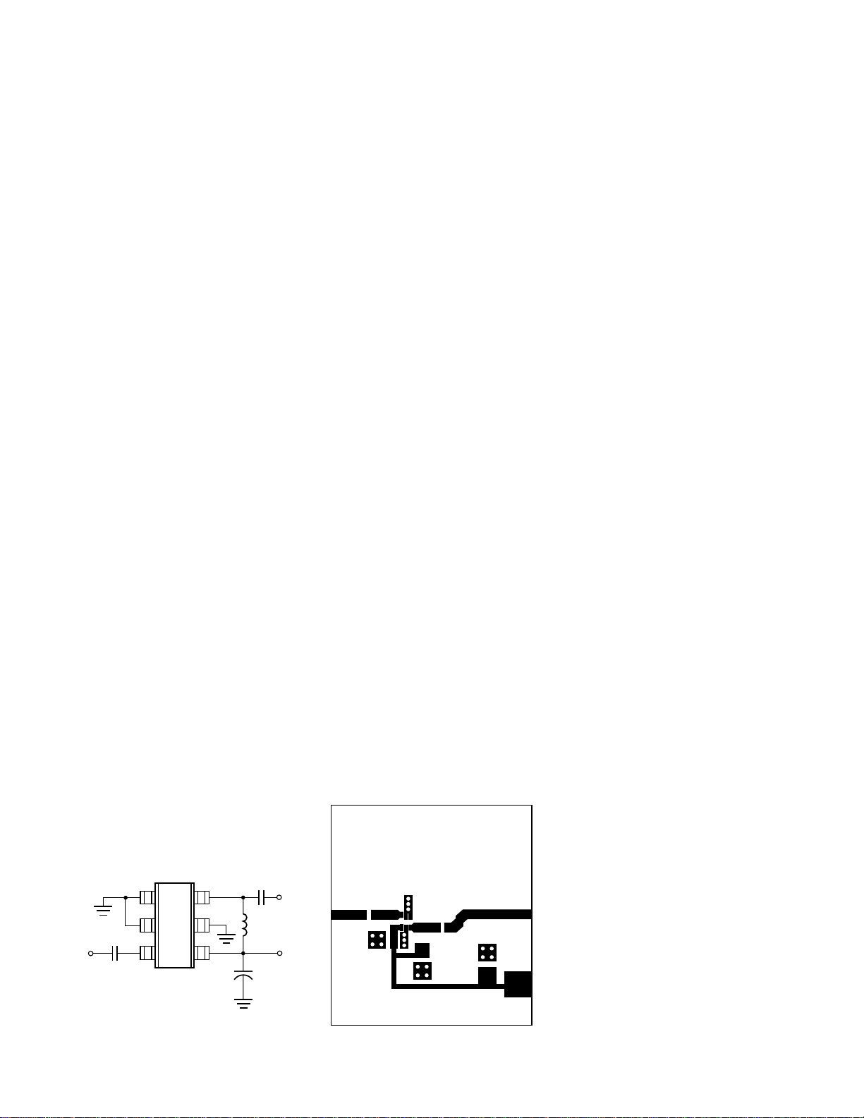
Figure 11 shows a typical implementation of the INA-52063. The
supply voltage for the INA-52063
must be applied to two terminals,
the VCC pin and the RF Output pin.
The VCC connection to the amplifier is RF bypassed by placing a
capacitor to ground near the V
pin of the amplifier package.
The power supply connection to
the RF Output pin is achieved by
means of a RF choke (inductor).
The value of the RF choke must
be large relative to 50 Ω in order
to prevent loading of the RF
Output.
The supply voltage end of the RF
choke is bypassed to ground with
a capacitor. If the physical layout
permits, this can be the same
bypass capacitor that is used at
the VCC terminal of the amplifier.
Blocking capacitors are normally
placed in series with the RF Input
and the RF Output to isolate the
DC voltages on these pins from
circuits adjacent to the amplifier.
The values for the blocking and
bypass capacitors are selected to
52
RF
C
INPUT
block
Figure 11. Basic Amplifier
Application.
C
RFC
block
C
bypass
CC
RF
OUTPUT
V
CC
provide a reactance at the lowest
frequency of operation that is
small relative to 50 Ω.
RF Layout
An example layout for an
amplifier using the INA-52063 is
shown in Figure 12.
This example uses a microstripline design (solid groundplane on
the back side of the circuit board).
The circuit board material is
0.031-inch thick FR-4. Plated
through holes (vias) are used to
bring the ground to the top side
of the circuit where needed.
Multiple vias are used to reduce
the inductance of the path to
ground.
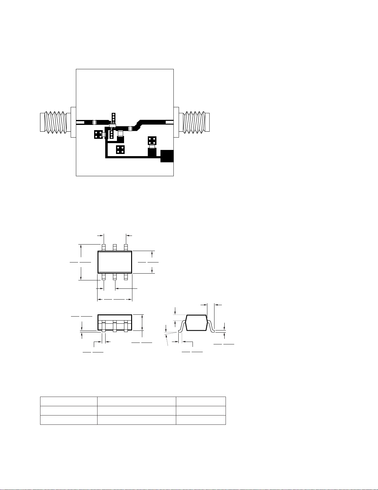
Figure 13 shows an assembled
amplifier. The +5 volt supply is
fed directly into the VCC pin of
the INA-52063 and into the RF
Output pin through the RF choke
(RFC). Capacitor C3 provides RF
bypassing for both the VCC pin
and the power supply end of the
RFC.
Capacitor C4 is optional and may
be used to add additional bypassing for the VCC line. A well
bypassed VCC line is especially
necessary in cascades of amplifier stages to prevent oscillation
that may occur as a result of RF
H
INA-5XX63 DEMO BOARD
INPUT OUTPUT
Figure 12. RF Layout.
05/95
V
CC
feedback through the power
supply lines.
For this demonstration circuit,
the value chosen for the RF
choke was 220 nH (Coilcraft
1008CS-221 or equivalent). All of
the blocking and bypass capacitors are 1000 pF. These values
provide excellent amplifier
performance from under 50 MHz
through 1 GHz. Larger values for
the choke and capacitors can be
used to extend the lower end of
the bandwidth. Since the gain of
the INA-52063 extends down to
DC, the frequency response of the
amplifier is limited only by the
values of the capacitors and
choke.
A convenient method for making
RF connection to the demonstration board is to use a PCB
mounting type of SMA connector
(Johanson 142-0701-881, or
equivalent). These connectors
can be slipped over the edge of
the PCB and the center conductors soldered to the input and
output lines. The ground pins of
the connectors are soldered to
the ground plane on the backside
of the board. The extra ground
pins for the top of the board are
not needed and are clipped off.
PCB Materials
Typical choices for PCB material
for low cost wireless applications
are FR-4 or G-10 with a thickness
of 0.025 or 0.031 inches. A thickness of 0.062 inches is the maximum that is recommended for
use with this particular device.
The use of a thicker board material increases the inductance of
the plated through vias used for
RF grounding and may deteriorate circuit performance. Adequate
grounding is needed not only to
obtain maximum amplifier
performance but also to reduce
any possibility of instability.
6-160
Page 6
H
INA-5XX63 DEMO BOARD
05/95
INPUT OUTPUT
C1
52
C3
Figure 13. Assembled Amplifier.
Package Dimensions
Outline 63 (SOT-363/SC-70)
1.30 (0.051)
REF.
2.20 (0.087)
2.00 (0.079)
2.20 (0.087)
1.80 (0.071)
C2
RFC
C4
V
CC
1.35 (0.053)
1.15 (0.045)
0.650 BSC (0.025)
0.425 (0.017)
TYP.
0.10 (0.004)
0.00 (0.00)
0.25 (0.010)
0.15 (0.006)
1.00 (0.039)
0.80 (0.031)
DIMENSIONS ARE IN MILLIMETERS (INCHES)
0.30 REF.
10°
0.30 (0.012)
0.10 (0.004)
INA-52063 Part Number Ordering Information
Part Number Devices per Container Container
INA-52063-TR1 3,000 7" reel
INA-52063-BLK 100 Antistatic bag
6-161
0.20 (0.008)
0.10 (0.004)
Page 7
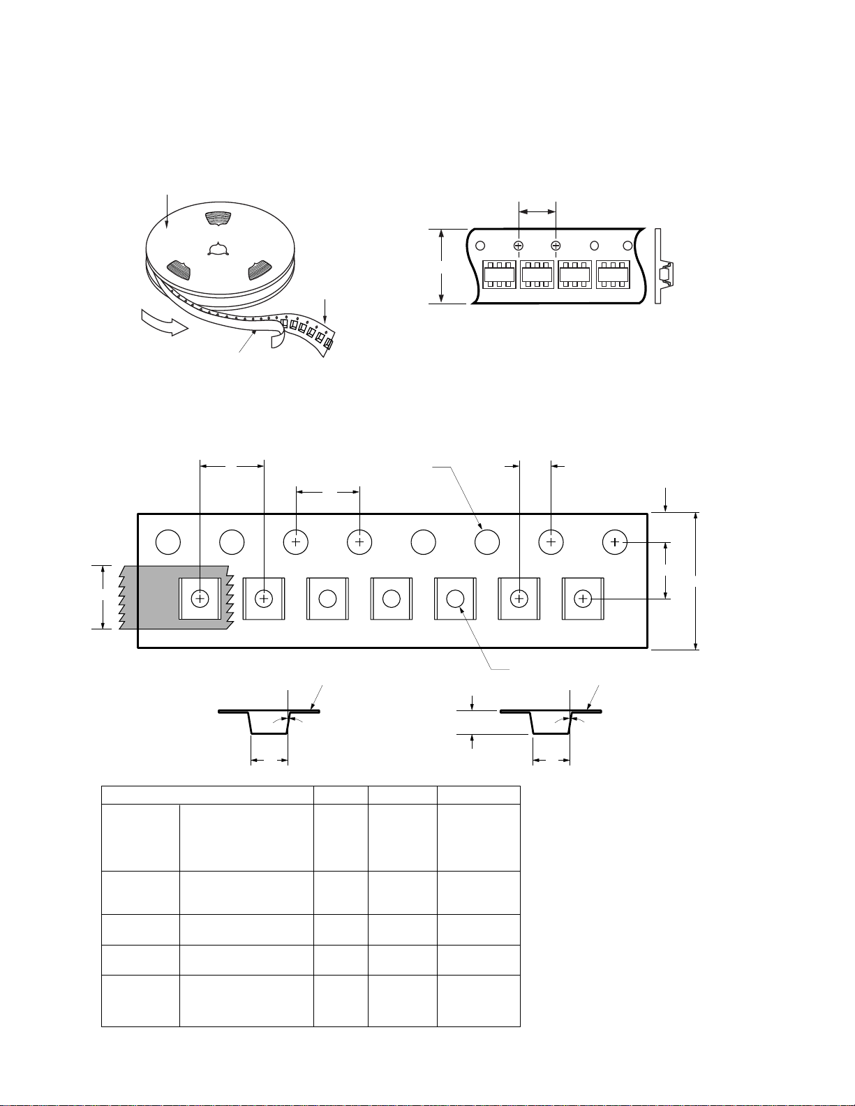
Device Orientation
REEL
TOP VIEW
4 mm
END VIEW
CARRIER
TAPE
USER
FEED
DIRECTION
COVER TAPE
Tape Dimensions and Product Orientation
For Outline 63
P
P
0
C
(CARRIER TAPE THICKNESS) Tt (COVER TAPE THICKNESS)
t
1
8 mm
D
52 52 52 52
P
2
D
1
E
F
W
CAVITY
PERFORATION
CARRIER TAPE
COVER TAPE
DISTANCE
8° MAX.
A
0
DESCRIPTION SYMBOL SIZE (mm) SIZE (INCHES)
A
LENGTH
WIDTH
DEPTH
PITCH
BOTTOM HOLE DIAMETER
DIAMETER
PITCH
POSITION
WIDTH
THICKNESS
WIDTH
TAPE THICKNESS
CAVITY TO PERFORATION
(WIDTH DIRECTION)
CAVITY TO PERFORATION
(LENGTH DIRECTION)
B
K
P
D
D
P
E
W
t
1
C
T
F
P
0
0
0
1
0
t
2
2.24 ± 0.10
2.34 ± 0.10
1.22 ± 0.10
4.00 ± 0.10
1.00 + 0.25
1.55 ± 0.05
4.00 ± 0.10
1.75 ± 0.10
8.00 ± 0.30
0.255 ± 0.013
5.4 ± 0.10
0.062 ± 0.001
3.50 ± 0.05
2.00 ± 0.05
K
0
0.088 ± 0.004
0.092 ± 0.004
0.048 ± 0.004
0.157 ± 0.004
0.039 + 0.010
0.061 ± 0.002
0.157 ± 0.004
0.069 ± 0.004
0.315 ± 0.012
0.010 ± 0.0005
0.205 ± 0.004
0.0025 ± 0.00004
0.138 ± 0.002
0.079 ± 0.002
6-162
5° MAX.
B
0
 Loading...