

Page 1
1 GHz Low Noise Silicon MMIC
Amplifier
Technical Data
INA-50311
Features
• Internally Biased, Single 5 V
Supply (17 mA)
• 19 dB Gain
• 3.6 dB NF
• Unconditionally Stable
SOT-143 Surface Mount Package
Applications
• Amplifier for Cellular,
Cordless, Special Mobile
Radio, PCS, ISM, Wireless
LAN, and TV Tuner
Applications
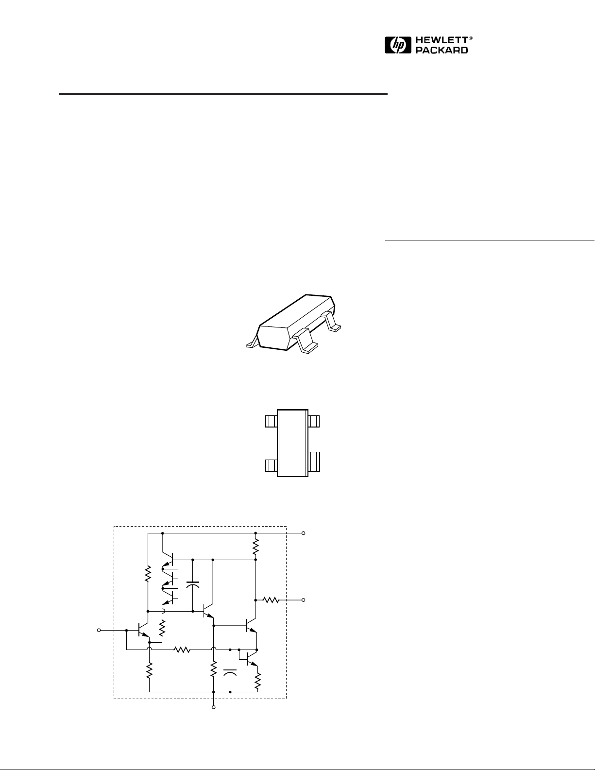
Pin Connections and Package Marking
Equivalent Circuit (Simplified)
INPUT
V
CC
N50
V
CC
GND
OUTPUT
Description
Hewlett-Packard’s INA-50311 is a
Silicon monolithic amplifier that
offers excellent gain and noise
figure for applications to 1.0 GHz.
Packaged in a miniature SOT-143
package, it requires very little
board space.
The INA-50311 uses a topology
which is internally biased,
eliminating the need for external
components and providing
decreased sensitivity to ground
inductance.
The INA-50311 is fabricated using
HP’s 30 GHz f
Silicon bipolar process which
uses nitride self-alignment submicrometer lithography, trench
isolation, ion implantation, gold
metallization, and polyimide
intermetal dielectric and scratch
protection to achieve superior
performance, uniformity, and
reliability.
MAX
ISOSAT
TM
RF
INPUT
5963-6680E
GROUND
RF
OUTPUT
6-146
Page 2

Absolute Maximum Ratings
Absolute
Symbol Parameter Units Maximum
V
CC
P
in
T
j
T
STG
INA-50311 Electrical Specifications
Device Voltage, to ground V 12
CW RF Input Power dBm +13
Junction Temperature °C 150
Storage Temperature °C -65 to 150
[3]
, T
= 25°C, ZO = 50 Ω, V
C
[1]
Thermal Resistance
θ
= 550°C/W
jc
Notes:
1. Operation of this device above any one
of these limits may cause permanent
damage.
2. T
= 25°C (T
C
temperature at the package pins where
contact is made to the circuit board).
= 5 V
CC
is defined to be the
C
Symbol Parameters and Test Conditions Units Min. Typ. Max.
G
p
Power Gain (|S21|2) f = 900 MHz dB 16.5 19
NF Noise Figure f = 900 MHz dB 3.6
P
1dB
IP
3
Output Power at 1 dB Gain Compression f = 900 MHz dBm 0
Third Order Intercept Point f = 900 MHz dBm +10
VSWR Input VSWR f = 900 MHz 1.5
Output VSWR f = 900 MHz 1.2
I
cc
ι
d
Device Current mA 17 22
Group Delay f = 900 MHz ps 320
[2]
:
INA-50311 Typical Scattering Parameters
Freq. S
11
S
21
[3]
, T
= 25°C, ZO = 50 Ω, V
C
S
12
CC
= 5 V
S
22
GHz Mag Ang dB Mag Ang dB Mag Ang Mag Ang Factor
0.05 0.12 -2 22.2 12.82 -6 -31.9 0.025 5 0.08 -11 1.68
0.10 0.12 -5 22.2 12.81 -12 -31.7 0.026 9 0.07 -24 1.63
0.20 0.12 -10 22.1 12.80 -24 -31.4 0.027 16 0.07 -44 1.59
0.30 0.14 -16 22.1 12.68 -36 -31.1 0.028 23 0.08 -62 1.55
0.40 0.15 -25 21.9 12.45 -49 -30.6 0.030 30 0.09 -78 1.48
0.50 0.16 -32 21.7 12.12 -61 -30.0 0.032 36 0.09 -94 1.44
0.60 0.17 -45 21.3 11.65 -74 -29.3 0.034 42 0.10 -107 1.42
0.70 0.18 -57 20.9 11.04 -87 -28.5 0.038 47 0.11 -120 1.36
0.80 0.19 -71 20.3 10.35 -99 -27.7 0.041 51 0.11 -131 1.35
0.90 0.19 -84 19.6 9.57 -111 -26.9 0.045 54 0.11 -141 1.34
1.00 0.20 -98 18.9 8.78 -122 -26.0 0.050 56 0.11 -149 1.32
1.20 0.21 -122 17.2 7.28 -143 -24.3 0.061 59 0.11 -163 1.31
1.40 0.21 -143 15.5 5.97 -161 -22.8 0.072 60 0.11 -172 1.33
1.60 0.21 -162 13.8 4.92 -176 -21.5 0.084 60 0.10 -179 1.37
1.80 0.22 -177 12.2 4.08 169 -20.4 0.095 58 0.10 175 1.42
2.00 0.22 170 10.7 3.43 157 -19.5 0.106 55 0.10 172 1.49
2.20 0.21 158 9.3 2.92 145 18.5 0.119 54 0.10 166 1.55
2.40 0.20 149 8.1 2.53 134 -17.9 0.127 50 0.11 163 1.65
2.50 0.20 146 7.5 2.37 129 -17.7 0.131 49 0.12 160 1.69
Note:
3. Reference plane per Figure 9 in Applications Information section.
K
6-147
Page 3
INA-50311 Typical Performance, T
P 1 dB (dBm)
0.1
-6
FREQUENCY (GHz)
0.7
6
0
-4
1.5
2
1.1
0.3 0.5 0.9 1.3
-2
4
5.5 V
5.0 V
4.5 V
= 25° C, ZO = 50 Ω, V
C
CC
= 5 V
25
20
15
10
GAIN (dB)
5
0
0.1
0.3 0.5 0.9 1.3
0.7
FREQUENCY (GHz)
1.1
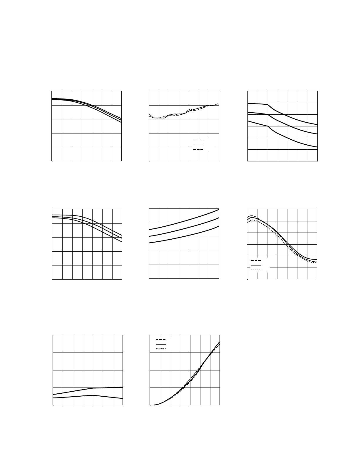
Figure 1. Power Gain vs. Frequency
and Voltage.
25
20
15
10
GAIN (dB)
5
0
0.1
0.3 0.5 0.9 1.3
0.7
FREQUENCY (GHz)
1.1
5
4
1.5
5.5 V
5.0 V
4.5 V
3
2
NOISE FIGURE (dB)
1
0
0.1
0.3 0.5 0.9 1.3
FREQUENCY (GHz)
0.7
Figure 2. Noise Figure vs. Frequency
and Voltage.
5
4
1.5
-40
+25
+85
3
2
NOISE FIGURE (dB)
1
0
0.1
0.3 0.5 0.9 1.3
FREQUENCY (GHz)
0.7
1.1
1.1
5.5 V
5.0 V
4.5 V
1.5
Figure 3. Output Power for 1 dB Gain
Compression vs. Frequency and
Voltage.
+85
+25
-40
1.5
3
2
1
0
-1
P 1 dB (dBm)
-2
-3
0.1
0.3 0.5 0.9 1.3
+85
+25
-40
0.7
FREQUENCY (GHz)
1.1
1.5
Figure 4. Gain vs. Frequency and
Temperature.
3.0
2.5
2.0
VSWR (N:1)
1.5
1.0
0.1
0.3 0.5 0.9 1.3
Figure 7. Input and Output VSWR vs.
Frequency.
0.7
FREQUENCY (GHz)
OUTPUT
1.1
INPUT
Figure 5. Noise Figure vs. Frequency
and Temperature.
1.5
40
30
20
(mA)
CC
I
10
0
0
+85
+25
-40
1 246
3
V
(V)
CC
Figure 8. Supply Current vs. Voltage
and Temperature.
6-148
Figure 6. Output Power for 1 dB Gain
Compression vs. Frequency and
Temperature.
5
7
Page 4
INA-50311 Applications Information
Introduction
INA-50311 is a silicon RF
integrated circuit amplifier with a
50 Ω input and output. The
INA-50311 uses resistive feedback
to provide flat gain for low noise
or multi-purpose gain block
applications up to 1000 MHz.
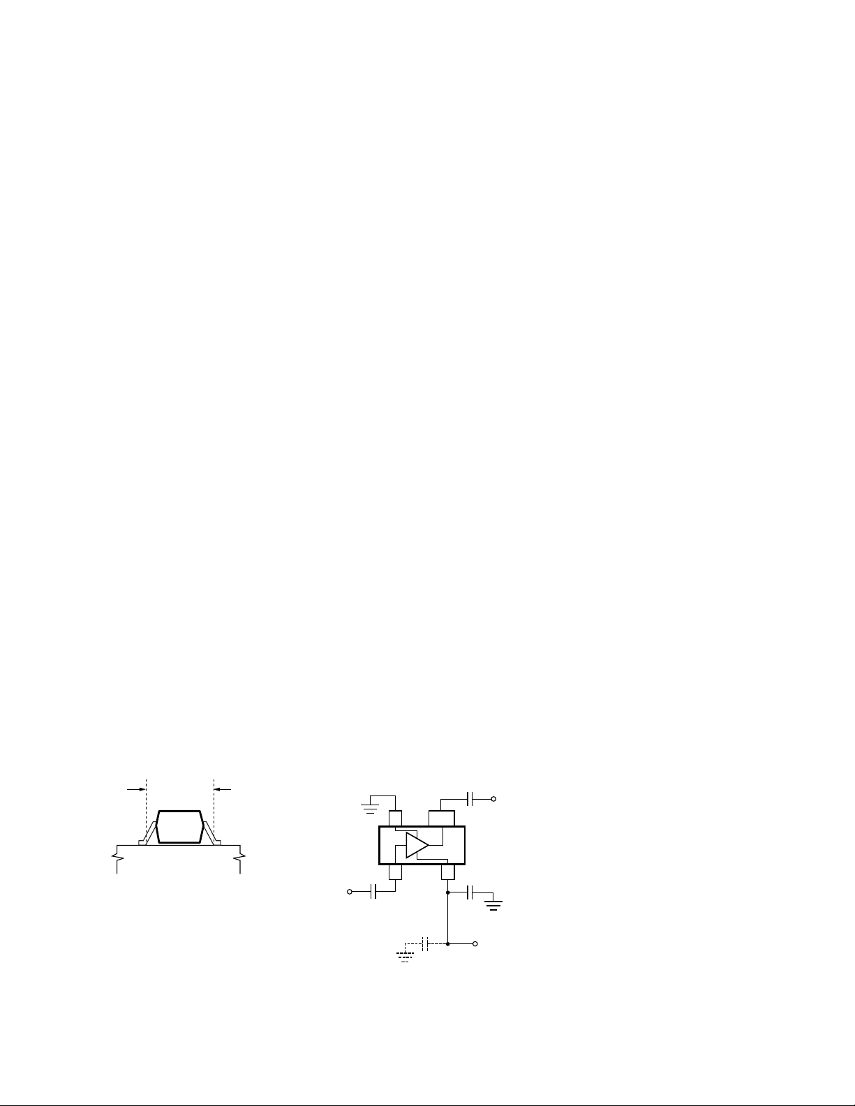
Phase Reference Planes
The positions of the reference
planes used to measure
S-Parameters are shown in
Figure 9. As seen in the illustration, the reference planes are
located at the point where the
package leads contact the test
circuit.
Biasing
The INA-50311 is a voltage biased
device and operates from a single
+5 volt power supply with a
current drain of only 17 mA. All
bias circuitry is fully integrated
into the IC eliminating the need
for external DC components. The
supply voltage for the INA-50311
is fed in through a separate V
pin of the device and does not
require RF isolation from the
input or output signal
connections.
REFERENCE
PLANES
TEST CIRCUIT
Figure 9. Reference Planes.
CC
Operating Details
The INA-50311 is very easy to use.
The basic application of the
INA-50311 is shown in Figure 10.
DC blocking capacitors are placed
in series with the RF Input and
RF Output to isolate adjacent
circuits from the internal bias
voltages that are present at these
terminals. The values of the
blocking capacitors are determined by the lowest operating
frequency. The values for the
blocking capacitors are chosen
such that their reactances are
small relative to 50 Ω. As an
example, use of the INA-50311 for
an application covering the 902 to
928 MHz band would require
blocking capacitors of at least
70␣ p F.
The VCC connection to the
amplifier must be RF bypassed by
placing a capacitor to ground
directly at the bias pin of the
package. Like the DC blocking
capacitors, the value of the V
CC
bypass capacitor is determined by
the lowest operating frequency
for the amplifier. This value may
typically be the same as that of
the DC blocking capacitors. If
long bias lines are used to connect the amplifier to the V
RF
C
INPUT
block
C
bypass
C
block
C
bypass
CC
OUTPUT
V
CC
RF
supply, additional bypass capacitors may be needed to prevent
resonances that would otherwise
result in undesirable gain
responses. A well-bypassed V
CC
line is also desirable to prevent
possible oscillations that may
occur due to feedback through
the bias line from other stages in
a cascade.
Adequate grounding is needed to
obtain maximum performance.
The ground pin of the INA-50311
should be connected directly to
RF ground by using plated
through holes (vias) near the
package terminals.
FR-4 or G-10 PCB material is a
good choice for most low cost
wireless applications. Typical
board thickness is 0.025 or 0.031
inches. The width of 50 Ω
microstriplines in these PCB
thicknesses is also convenient for
mounting chip components such
as the series DC blocking
capacitors.
Circuit Example
The amplifier example in Figure
11 shows a typical implementation of the INA-50311. The input
and output connections are
through 50 Ω microstriplines with
DC blocking capacitors.
The VCC supply connection is RF
bypassed very close to the lead of
the RFIC. Provision is also made
for an additional bypass capacitor
on the VCC line near the edge of
the PCB.
Figure 10. Basic Amplifier
Application.
6-149
Page 5
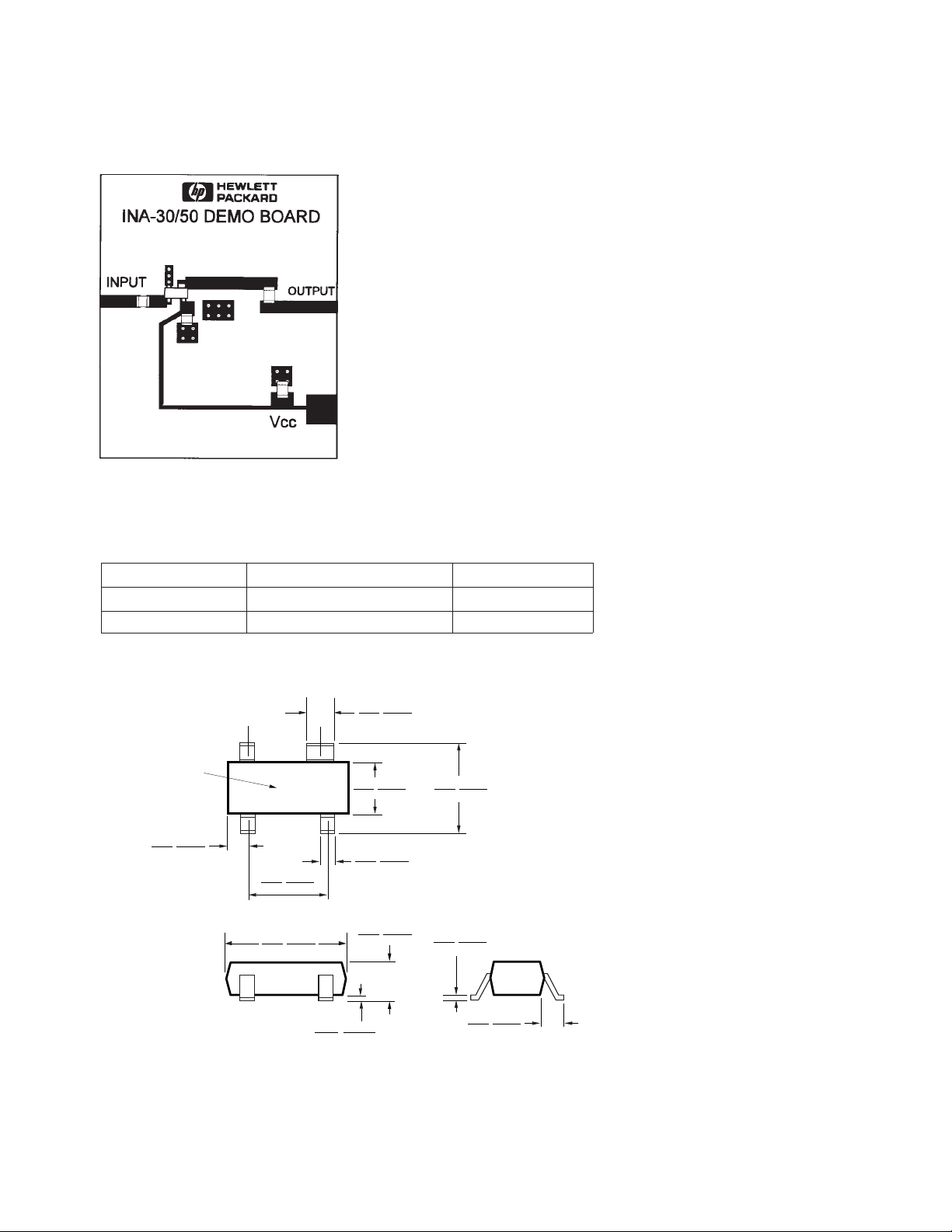
Figure 11. Application Example.
INA-50311 Part Number Ordering Information
Part Number Devices per Container Container
INA-50311-TR1 3,000 7" reel
INA-50311-BLK 100 Antistatic bag
Package Dimensions
0.92 (0.036)
0.78 (0.031)
PACKAGE
MARKING
CODE
0.60 (0.024)
0.45 (0.018)
XXX
2.04 (0.080)
1.78 (0.070)
TOP VIEW
3.06 (0.120)
2.80 (0.110)
1.40 (0.055)
1.20 (0.047)
0.54 (0.021)
0.37 (0.015)
1.02 (0.041)
0.85 (0.033)
2.65 (0.104)
2.10 (0.083)
0.15 (0.006)
0.09 (0.003)
0.10 (0.004)
0.013 (0.0005)
DIMENSIONS ARE IN MILLIMETERS (INCHES)
0.69 (0.027)
0.45 (0.018)
6-150
END VIEWSIDE VIEW
 Loading...