

Datasheet INA122UA-2K5, INA122UA, INA122U-2K5, INA122PA, INA122P Datasheet (Burr Brown)
...Page 1
©1997 Burr-Brown Corporation PDS-1388B Printed in U.S.A. October, 1997
100kΩ
25kΩ
25kΩ
100kΩ
INA122
5
4
2
1
8
3
7
6
R
G
V
IN
–
V
IN
+
V+
V
O
Ref
V–
200k
R
G
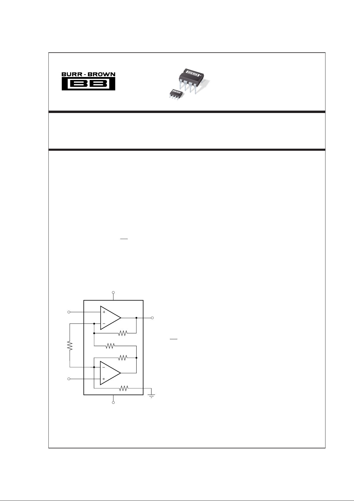
G = 5 +
V
O
= (VIN – VIN) G
–+
®
INA122
Single Supply,
Micro
Power
INSTRUMENTATION AMPLIFIER
FEATURES
● LOW QUIESCENT CURRENT: 60µA
● WIDE POWER SUPPLY RANGE
Single Supply: 2.2V to 36V
Dual Supply: –0.9/+1.3V to
±18V
● COMMON-MODE RANGE TO (V–)–0.1V
● RAIL-TO-RAIL OUTPUT SWING
● LOW OFFSET VOLTAGE: 250
µV max
● LOW OFFSET DRIFT: 3
µV/°C max
● LOW NOISE: 60nV/√Hz
● LOW INPUT BIAS CURRENT: 25nA max
● 8-PIN DIP AND SO-8 SURFACE-MOUNT
APPLICATIONS
● PORTABLE, BATTERY OPERATED
SYSTEMS
● INDUSTRIAL SENSOR AMPLIFIER:
Bridge, RTD, Thermocouple
● PHYSIOLOGICAL AMPLIFIER:
ECG, EEG, EMG
● MULTI-CHANNEL DATA ACQUISITION
INA122
INA122
International Airport Industrial Park • Mailing Address: PO Box 11400, Tucson, AZ 85734 • Street Address: 6730 S. Tucson Blvd., Tucson, AZ 85706 • Tel: (520) 746-1111 • Twx: 910-952-1111
Internet: http://www.burr-brown.com/ • FAXLine: (800) 548-6133 (US/Canada Only) • Cable: BBRCORP • Telex: 066-6491 • FAX: (520) 889-1510 • Immediate Product Info: (800) 548-6132
DESCRIPTION
The INA122 is a precision instrumentation amplifier
for accurate, low noise differential signal acquisition.
Its two-op-amp design provides excellent performance
with very low quiescent current, and is ideal for
portable instrumentation and data acquisition systems.
The INA122 can be operated with single power supplies from 2.2V to 36V and quiescent current is a mere
60µA. It can also be operated from dual supplies. By
utilizing an input level-shift network, input commonmode range extends to 0.1V below negative rail (single
supply ground).
A single external resistor sets gain from 5V/V to
10000V/V. Laser trimming provides very low offset
voltage (250µV max), offset voltage drift (3µV/°C
max) and excellent common-mode rejection.
Package options include 8-pin plastic DIP and SO-8
surface-mount packages. Both are specified for the
–40°C to +85°C extended industrial temperature range.
Page 2
2
®
INA122
SPECIFICATIONS
At TA = +25°C, VS = +5V, RL = 20kΩ connected to VS/2, unless otherwise noted.
The information provided herein is believed to be reliable; however, BURR-BROWN assumes no responsibility for inaccuracies or omissions. BURR-BROWN assumes
no responsibility for the use of this information, and all use of such information shall be entirely at the user’s own risk. Prices and specifications are subject to change
without notice. No patent rights or licenses to any of the circuits described herein are implied or granted to any third party. BURR-BROWN does not authorize or warrant
any BURR-BROWN product for use in life support devices and/or systems.
INA122P, U INA122PA, UA
PARAMETER CONDITIONS MIN TYP MAX MIN TYP MAX UNITS
INPUT
Offset Voltage, RTI ±100 ±250 ±150 ±500 µV
vs Temperature ±1 ±3 ✻ ±5 µV/°C
vs Power Supply (PSRR) V
S
= +2.2V to +36V 10 30 ✻ 100 µV/V
Input Impedance 10
10
|| 3 ✻ Ω || pF
Safe Input Voltage R
S
= 0 (V–)–0.3 (V+)+0.3 ✻✻V
R
S
= 10kΩ (V–)–40 (V+)+40 ✻✻V
Common-Mode Voltage Range 0 3.4 ✻✻V
Common-Mode Rejection V
CM
= 0V to 3.4V 83 96 76 90 dB
INPUT BIAS CURRENT –10 –25 ✻ –50 nA
vs Temperature ±40 ✻ pA/°C
Offset Current ±1 ±2 ✻ ±5nA
vs Temperature ±40 ✻ pA/°C
GAIN G = 5 to 10k ✻ V/V
Gain Equation G = 5 + 200kΩ/R
G
✻ V/V
Gain Error G = 5 ±0.05 ±0.1 ✻ ±0.15 %
vs Temperature G = 5 5 10 ✻✻ppm/°C
Gain Error G = 100 ±0.3 ±0.5 ✻ ±1%
vs Temperature G = 100 ±25 ±100 ✻✻ppm/°C
Nonlinearity
G = 100, VO = –14.85V to +14.9V
±0.005 ±0.012 ✻ ±0.024 %
NOISE (RTI)
Voltage Noise, f = 1kHz 60 ✻ nV/√Hz
f = 100Hz 100 ✻ nV/√Hz
f = 10Hz 110 ✻ nV/√Hz
f
B
= 0.1Hz to 10Hz 2 ✻ µVp-p
Current Noise, f = 1kHz 80 ✻ fA/√Hz
f
B
= 0.1Hz to 10Hz 2 ✻ pAp-p
OUTPUT
Voltage, Positive V
S
= ±15V (V+)–0.1 (V+)–0.05 ✻✻ V
Negative V
S
= ±15V (V–)+0.15 (V–)+0.1 ✻✻ V
Short-Circuit Current Short-Circuit to Ground +3/–30 ✻ mA
Capacitive Load Drive 1 ✻ nF
FREQUENCY RESPONSE
Bandwidth, –3dB G = 5 120 ✻ kHz
G = 100 5 ✻ kHz
G = 500 0.9 ✻ kHz
Slew Rate
+0.08/–0.16
✻ V/µs
Settling Time, 0.01% G = 5 350 ✻ µs
G = 100 450 ✻ µs
G = 500 1.8 ✻ ms
Overload Recovery 50% Input Overload 3 ✻ µs
POWER SUPPLY
Voltage Range, Single Supply +2.2 +5 +36 ✻✻✻ V
Dual Supplies –0.9/+1.3 ±18 ✻✻✻ V
Current I
O
= 0 60 8 5 ✻✻ µA
TEMPERATURE RANGE
Specification –40 +85 ✻✻°C
Operation –55 +85 ✻✻°C
Storage –55 +125 ✻✻°C
Thermal Resistance,
θ
JA
8-Pin DIP 150 ✻ °C/W
SO-8 Surface-Mount 150 ✻ °C/W
✻ Specification same as INA122P, INA122U.
Page 3
3
®
INA122
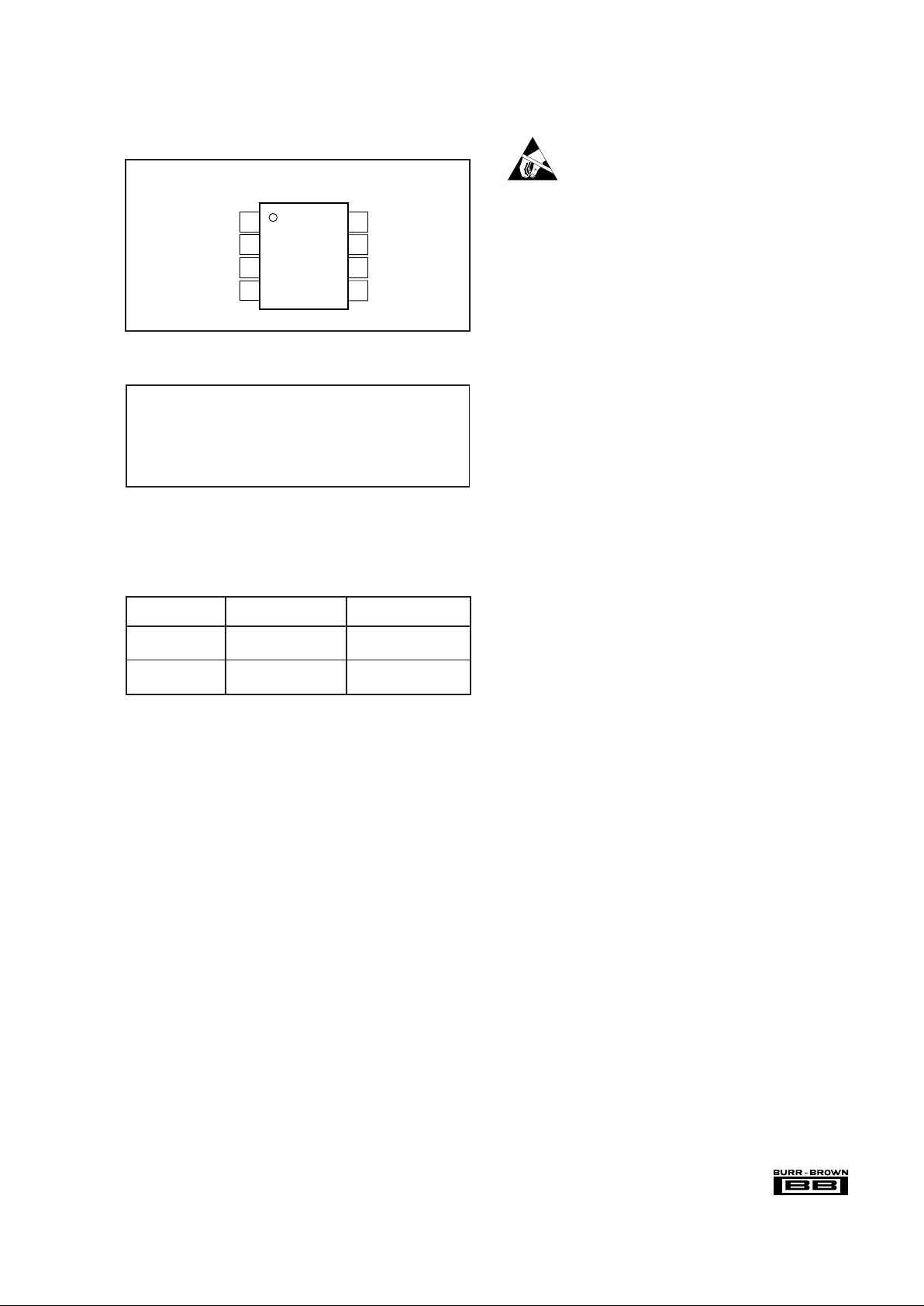
PIN CONFIGURATION
Top View 8-Pin DIP, SO-8
Supply Voltage, V+ to V– .................................................................... 36V
Signal Input Terminals, Voltage
(2)
....................... (V–)–0.3V to (V+)+0.3V
Current
(2)
...................................................... 5mA
Output Short Circuit ................................................................. Continuous
Operating Temperature ................................................. –40°C to +125°C
Storage Temperature ..................................................... –55°C to +125°C
Lead Temperature (soldering, 10s)............................................... +300°C
NOTES: (1) Stresses above these ratings may cause permanent damage.
(2) Input terminals are internally diode-clamped to the power supply rails.
Input signals that can exceed the supply rails by more than 0.3V should be
current-limited to 5mA or less.
ABSOLUTE MAXIMUM RATINGS
(1)
PACKAGE INFORMATION
PACKAGE DRAWING
PRODUCT PACKAGE NUMBER
(1)
INA122PA 8-Pin DIP 006
INA122P 8-Pin DIP 006
INA122UA SO-8 Surface Mount 182
INA122U SO-8 Surface Mount 182
NOTE: (1) For detailed drawing and dimension table, see end of data sheet, or
Appendix C of Burr-Brown IC Data Book.
ELECTROSTATIC
DISCHARGE SENSITIVITY
This integrated circuit can be damaged by ESD. Burr-Brown
recommends that all integrated circuits be handled with appropriate precautions. Failure to observe proper handling and
installation procedures can cause damage.
ESD damage can range from subtle performance degradation
to complete device failure. Precision integrated circuits may
be more susceptible to damage because very small parametric
changes could cause the device not to meet its published
specifications.
R
G
V
IN
V
IN
V–
R
G
V+
V
O
Ref
1
2
3
4
8
7
6
5
–
+
Page 4

4
®
INA122
TYPICAL PERFORMANCE CURVES
At TA = +25°C and VS = ±5V, unless otherwise noted.
GAIN vs FREQUENCY
70
60
50
40
30
20
10
0
–10
Gain (dB)
Frequency (Hz)
100 1k 10k 100k 1M
G = 1000
G = 100
G = 20
G = 5
COMMON-MODE REJECTION vs FREQUENCY
110
100
90
80
70
60
50
40
30
20
10
0
Common-Mode Rejection (dB)
Frequency (Hz)
1 10 100 1k 10k 100k
G = 1000
G = 100
G = 5
NEGATIVE POWER SUPPLY REJECTION
vs FREQUENCY
100
80
60
40
20
0
Power Supply Rejection (dB)
Frequency (Hz)
1 10 100 1k 10k 100k
G = 500
G = 5
G = 100
POSITIVE POWER SUPPLY REJECTION
vs FREQUENCY
100
80
60
40
20
0
Power Supply Rejection (dB)
Frequency (Hz)
10 100 1k 10k 100k 1M
G = 500
G = 100
G = 5
INPUT COMMON-MODE RANGE
vs OUTPUT VOLTAGE, V
S
= ±15V, G = 5
Output Voltage (V)
Common-Mode Voltage (V)
–15 –10 0 5 15–5
15
10
5
0
–5
–10
–15
10
V
D/2
+
+
–
–
V
CM
V
O
V
D/2
Ref
–15V
+15V
+
Limited by A
2
output swing—see text
INPUT COMMON-MODE VOLTAGE
vs OUTPUT VOLTAGE, V
S
= ±5V, G = 5
Output Voltage (V)
Input Common-Mode Voltage (V)
–5 –4 5–3 –2 –1 0 1 2 3 4
5
4
3
2
1
0
–1
–2
–3
–4
–5
Limited by A
2
output swing—see text
VS = ±5V
VS = +5V/0V
V
REF
= 2.5V
V
REF
= 0V
Page 5

5
®
INA122
TYPICAL PERFORMANCE CURVES (CONT)
At TA = +25°C and VS = ±5V, unless otherwise noted.
QUIESCENT CURRENT vs TEMPERATURE
Temperature (°C)
Quiescent Current (µA)
–75 –50 –25 0 25 50 12575 100
80
60
40
20
0
SETTLING TIME vs GAIN
Gain (V/V)
Settling Time (ms)
10
1
0.1
1 10 100 1k
0.01%
10V Step
0.1%
INPUT-REFERRED OFFSET VOLTAGE WARM-UP
Time After Turn-On (ms)
Offset Voltage Change (µV)
01 1023456789
10
8
6
4
2
0
–2
–4
–6
–8
–10
(Noise)
Turn-on time ≤ 1ms. Settling time to
final value depends on Gain—see
settling time.
TOTAL HARMONIC DISTORTION+NOISE
vs FREQUENCY
Frequency (Hz)
THD+N (%)
10 100 1k
1
0.1
0.01
0.001
10k
G = 5
G = 100
RL = ∞
R
L
= 25kΩ
VOLTAGE and CURRENT NOISE DENSITY
vs FREQUENCY (RTI)
1000
100
10
Current Noise (fA/√Hz)
Frequency (Hz)
1 10 100 10k1k
Voltage Noise (nV/√Hz)
V
N
I
N
OUTPUT VOLTAGE SWING
vs OUTPUT CURRENT
0 5 10 15 20 25
Output Current (mA)
Output Voltage (V)
Sourcing Current
Sinking Current
V+
(V+)–1
(V+)–2
(V–)+2
(V–)+1
V–
Page 6

6
®
INA122
TYPICAL PERFORMANCE CURVES (CONT)
At TA = +25°C and VS = ±5V, unless otherwise noted.
50µs/div
100mV/div
SMALL-SIGNAL STEP RESPONSE
G = 5
100µs/div
100mV/div
SMALL-SIGNAL STEP RESPONSE
G = 100
50µs/div
2V/div
LARGE-SIGNAL STEP RESPONSE
G = 5
500ms/div
2µV/div
INPUT-REFERRED NOISE VOLTAGE
0.1Hz to 10Hz
Page 7

7
®
INA122
APPLICATION INFORMATION
Figure 1 shows the basic connections required for operation
of the INA122. Applications with noisy or high impedance
power supplies may require decoupling capacitors close to
the device pins.
The output is referred to the output reference (Ref) terminal
which is normally grounded. This must be a low-impedance
connection to ensure good common-mode rejection. A resistance of 10Ω in series with the Ref pin will cause a typical
device to degrade to approximately 80dB CMR.
SETTING THE GAIN
Gain of the INA122 is set by connecting a single external
resistor, R
G
, as shown:
(1)
Commonly used gains and R
G
resistor values are shown in
Figure 1.
The 200kΩ term in equation 1 comes from the internal metal
film resistors which are laser trimmed to accurate absolute
values. The accuracy and temperature coefficient of these
resistors are included in the gain accuracy and drift specifications of the INA122.
The stability and temperature drift of the external gain
setting resistor, R
G
, also affects gain. RG’s contribution to
gain accuracy and drift can be directly inferred from the gain
equation (1).
OFFSET TRIMMING
The INA122 is laser trimmed for low offset voltage and
offset voltage drift. Most applications require no external
offset adjustment. Figure 2 shows an optional circuit for
trimming the output offset voltage. The voltage applied to
the Ref terminal is added to the output signal. An op amp
buffer is used to provide low impedance at the Ref terminal
to preserve good common-mode rejection.
G
k
R
G
=+5
200 Ω
FIGURE 1. Basic Connections.
100kΩ
25kΩ
25kΩ
100kΩ
INA122
5
4
2
3
6
5
8
1
2
1
8
3
7
6
R
G
R
G
V
IN
A
2
A
1
–
V
IN
+
V
IN
–
V
IN
+
V+
V–
INA122
0.22µF
0.1µF
V
O
V
O
Ref
Ref
Load
+
–
Also drawn in simplified form:
VO = (VIN – VIN) G
–+
200kΩ
R
G
G = 5 +
Dual Supply
Single Supply
DESIRED GAIN RGNEAREST 1%
(V/V) (Ω)R
G
VALUE
5NCNC
10 40k 40.2k
20 13.33k 13.3k
50 4444 4420
100 2105 2100
200 1026 1020
500 404 402
1000 201 200
2000 100.3 100
5000 40 40.2
10000 20 20
NC: No Connection.
INPUT BIAS CURRENT RETURN PATH
The input impedance of the INA122 is extremely high—
approximately 10
10
Ω. However, a path must be provided for
the input bias current of both inputs. This input bias current
is approximately –10nA (current flows out of the input
terminals). High input impedance means that this input bias
current changes very little with varying input voltage.
FIGURE 2. Optional Trimming of Output Offset Voltage.
10kΩ
OPA336
±10mV
Adjustment Range
100Ω
100Ω
100µA
1/2 REF200
100µA
1/2 REF200
V+
V–
R
G
INA122
Ref
V
O
V
IN
–
V
IN
+
Page 8

8
®
INA122
Input circuitry must provide a path for this input bias current
for proper operation. Figure 3 shows various provisions for an
input bias current path. Without a bias current path, the inputs
will float to a potential which exceeds the common-mode
range of the INA122 and the input amplifiers will saturate.
If the differential source resistance is low, the bias current
return path can be connected to one input (see the thermocouple example in Figure 3). With higher source impedance,
using two equal resistors provides a balanced input with
possible advantages of lower input offset voltage due to bias
current and better high-frequency common-mode rejection.
INPUT PROTECTION
The inputs of the INA122 are protected with internal diodes
connected to the power supply rails (Figure 4). These diodes
will clamp the applied signal to prevent it from damaging the
input circuitry. If the input signal voltage can exceed the
power supplies by more than 0.3V, the input signal current
should be limited to less than 5mA to protect the internal
clamp diodes. This can generally be done with a series input
resistor. Some signal sources are inherently current-limited
and do not require limiting resistors.
INPUT COMMON-MODE RANGE
The common-mode range for some common operating conditions is shown in the typical performance curves. The
INA122 can operate over a wide range of power supply and
V
REF
configurations, making it impractical to provide a
comprehensive guide to common-mode range limits for all
possible conditions. The most commonly overlooked overload condition occurs by attempting to exceed the output
swing of A2, an internal circuit node that cannot be measured. Calculating the expected voltages at A
2
’s output (see
equation in Figure 4) provides a check for the most common
overload conditions.
The design of A
1
and A2 are identical and their outputs can
swing to within approximately 100mV of the power supply
rails, depending on load conditions. When A2’s output is
saturated, A
1
can still be in linear operation, responding to
changes in the non-inverting input voltage. This may give the
appearance of linear operation but the output voltage is invalid.
A single supply instrumentation amplifier has special design
considerations. Using commonly available single-supply op
amps to implement the two-op amp topology will not yield
equivalent performance. For example, consider the condition
where both inputs of common single-supply op amps are
FIGURE 4. INA122 Simplified Circuit Diagram.
47kΩ47kΩ
10kΩ
Microphone,
Hydrophone
etc.
Thermocouple
Center-tap provides
bias current return.
INA122
INA122
INA122
FIGURE 3. Providing an Input Common-Mode Current Path.
100kΩ
25kΩ
25kΩ
100kΩ
(8)
(1)
R
G
V
IN
+
V
IN
V
02
–
V+
V–
V
O
VO2 = 1.25VIN – (V
IN
– VIN) + 0.6V
––
+
25kΩ
R
G
(3)
V
IN
+ 0.5V
–
V
IN
+ 0.5V
+
V+
V–
A
1
A
2
(2)
(Voltages are referred to V
REF
)
(V–) + 0.1V ≤ V
02
≤ (V+) –0.1V
Ref
Page 9

9
®
INA122
equal to 0V. The outputs of both A1 and A2 must be 0V. But
any small positive voltage applied to V
IN
+
requires that A2’s
output must swing below 0V, which is clearly impossible
without a negative power supply.
To achieve common-mode range that extends to singlesupply ground, the INA122 uses precision level-shifting
buffers on its inputs. This shifts both inputs by approximately +0.5V, and through the feedback network, shifts A
2
’s
output by approximately +0.6V. With both inputs and V
REF
at single-supply, A2’s output is well within its linear range.
A positive V
IN
+
causes A2’s output to swing below 0.6V.
As a result of this input level-shifting, the voltages at pin 1
and pin 8 are not equal to their respective input terminal
voltages (pins 2 and 3). For most applications, this is not
important since only the gain-setting resistor connects to
these pins.
LOW VOLTAGE OPERATION
The INA122 can be operated on a single power supply as
low as +2.2V (or a total of +2.2V on dual supplies). Performance remains excellent throughout the power supply range
up to +36V (or ±18V). Most parameters vary only slightly
throughout this supply voltage range—see typical performance curves.
Operation at very low supply voltage requires careful attention to ensure that the common-mode voltage remains within
its linear range.
LOW QUIESCENT CURRENT OPERATION
The INA122 maintains its low quiescent current (60µA)
while the output is within linear operation (up to 200mV
from the supply rails). When the input creates a condition
that overdrives the output into saturation, quiescent current
increases. With V
O
overdriven into the positive rail, the
quiescent current increases to approximately 400µA. Likewise, with VO overdriven into the negative rail (single
supply ground) the quiescent current increases to approximately 200µA.
OUTPUT CURRENT RANGE
Output sourcing and sinking current values versus the output
voltage ranges are shown in the typical performance curves.
The positive and negative current limits are not equal.
Positive output current sourcing will drive moderate to high
load impedances. Battery operation normally requires the
careful management of power consumption to keep load
impedances very high throughout the design.
FIGURE 6. Single-Supply Current Shunt Measurement.
INA122
ADS7816
12-Bit A/D
V
IN
R
G
R
S
0.02Ω
I
L
2.5A
+
V
IN
–
3
2
4
5
6
7
G = 100
1
8
+5V
V+
Differential measurement
avoids ground loop errors.
Load
Shunt
7
5
6
8
4
2
1
3
Chip Select
Clock
Serial Data
CS
CLK
D
V
REF
+IN
–IN
1kΩ
0.47µF
50mV
FIGURE 5. Micropower Single Supply Bridge Amplifier.
1kΩ
REF200
200µA
INA122
3
8
7
4
5
6
2
1
VCM ≈ 100mV
≈ 200mV
V
IN
+
V
IN
R
G
VO = 0.1V to 4.9V
V
O
–
(60µA)
Ref
(1)
+5V
NOTE: (1) To accomodate bipolar input signals,
V
REF
can be offset to a positive voltage. Output
voltage is then referred to the voltage applied to Ref.
 Loading...