

Page 1

1
®
INA121
International Airport Industrial Park • Mailing Address: PO Box 11400, Tucson, AZ 85734 • Street Address: 6730 S. Tucson Blvd., Tucson, AZ 85706 • Tel: (520) 746-1111 • Twx: 910-952-1111
Internet: http://www.burr-brown.com/ • FAXLine: (800) 548-6133 (US/Canada Only) • Cable: BBRCORP • Telex: 066-6491 • FAX: (520) 889-1510 • Immediate Product Info: (800) 548-6132
®
INA121
INA121
INA121
©1997 Burr-Brown Corporation PDS-1412A Printed in U.S.A. May, 1998
FEATURES
● LOW BIAS CURRENT: ±4pA
● LOW QUIESCENT CURRENT:
±450µA
● LOW INPUT OFFSET VOLTAGE:
±200µV
● LOW INPUT OFFSET DRIFT:
±2µV/°C
● LOW INPUT NOISE:
20nV/√Hz at f = 1kHz (G =100)
● HIGH CMR: 106dB
● WIDE SUPPLY RANGE:
±2.25V to ±18V
● LOW NONLINEARITY ERROR: 0.001% max
● INPUT PROTECTION TO
±40V
● 8-PIN DIP AND SO-8 SURFACE MOUNT
FET-Input, Low Power
INSTRUMENTATION AMPLIFIER
DESCRIPTION
The INA121 is a FET-input, low power instrumentation amplifier offering excellent accuracy. Its versatile
three-op amp design and very small size make it ideal
for a variety of general purpose applications. Low bias
current (±4pA) allows use with high impedance
sources.
Gain can be set from 1V to 10,000V/V with a single
external resistor. Internal input protection can withstand up to ±40V without damage.
The INA121 is laser-trimmed for very low offset
voltage (±200µV), low offset drift (±2µV/°C), and
high common-mode rejection (106dB at G = 100). It
operates on power supplies as low as ±2.25V (+4.5V),
allowing use in battery operated and single 5V systems. Quiescent current is only 450µA.
Package options include 8-pin plastic DIP and SO-8
surface mount. All are specified for the –40°C to
+85°C industrial temperature range.
APPLICATIONS
● LOW-LEVEL TRANSDUCER AMPLIFIERS
Bridge, RTD, Thermocouple
● PHYSIOLOGICAL AMPLIFIERS
ECG, EEG, EMG, Respiratory
● HIGH IMPEDANCE TRANSDUCERS
● CAPACITIVE SENSORS
● MULTI-CHANNEL DATA ACQUISITION
● PORTABLE, BATTERY OPERATED SYSTEMS
● GENERAL PURPOSE INSTRUMENTATION
A
1
A
2
A
3
6
40kΩ40kΩ
40kΩ40kΩ
7
4
3
8
1
2
V
IN
V
IN
R
G
V+
V–
INA121
Ref
V
O
G = 1 +
50kΩ
R
G
–
+
5
Over-Voltage
Protection
25kΩ
25kΩ
Over-Voltage
Protection
Page 2
2
®
INA121
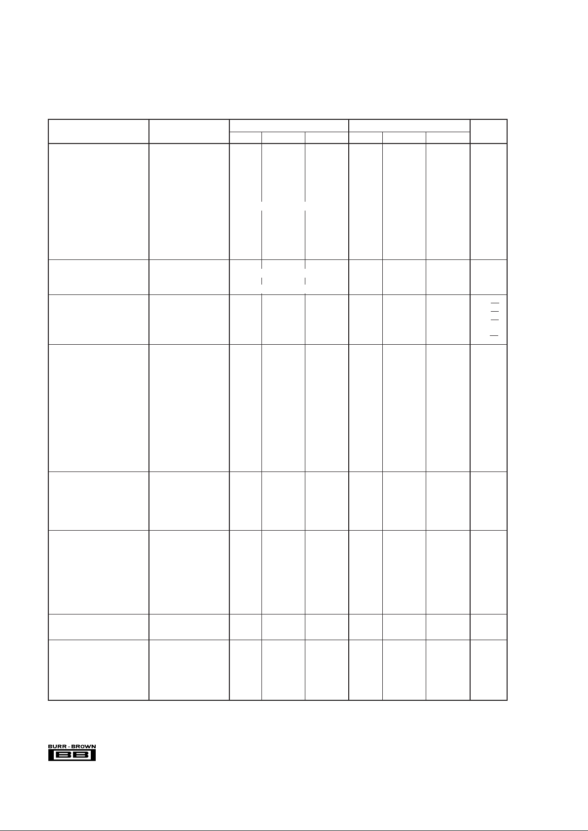
SPECIFICATIONS: VS = ±15V
At TA = +25°C, VS = ±15V, RL = 10kΩ, and IA reference = 0V, unless otherwise noted.
✻ Specification same as INA121P, U.
NOTE: (1) Temperature coefficient of the “Internal Resistor” in the gain equation. Does not include TCR of gain-setting resistor, R
G
.
INA121P, U INA121PA, UA
PARAMETER CONDITIONS MIN TYP MAX MIN TYP MAX UNITS
INPUT
Offset Voltage, RTI ±200±200/G ±500±500/G ±300±200/G
±1000±1000/G
µV
vs Temperature ±2±2/G ±5±20/G ✻ ±15±20/G µV/°C
vs Power Supply V
S
= ±2.25V to ±18V ±5±20/G ±50±150/G ✻✻µV/V
Long-Term Stability ±0.5 ✻ µV/mo
Impedance, Differential 10
12
|| 1 ✻ Ω || pF
Common-Mode V
O
= 0V 10
12
|| 12 ✻ Ω || pF
Input Voltage Range See Text and Typical Curves ✻
Safe Input Voltage ±40 ✻ V
Common-Mode Rejection V
CM
= –12.5V to 13.5V
G = 1 78 86 72 ✻ dB
G = 10 91 100 85 ✻ dB
G = 100 96 106 90 ✻ dB
G = 1000 106 ✻ dB
BIAS CURRENT V
CM
= 0V ±4 ±50 ✻✻pA
vs Temperature See Typical Curve ✻
Offset Current ±0.5 ✻ pA
vs Temperature See Typical Curve ✻
NOISE, RTI R
S
= 0Ω
Voltage Noise: f = 10Hz G = 100 30 ✻ nV/√Hz
f = 100Hz G = 100 21 ✻ nV/√Hz
f = 1kHz G = 100 20 ✻ nV/√Hz
f
= 0.1Hz to 10Hz G = 100 1 ✻ µVp-p
Current Noise: f = 1kHz 1 ✻ fA/√Hz
GAIN
Gain Equation 1 + (50kΩ/R
G
) ✻ V/V
Range of Gain 1 10,000 ✻✻V/V
Gain Error V
O
= –14V to 13.5V
G = 1 ±0.01 ±0.05 ✻ ±0.1 %
G = 10 ±0.03 ±0.4 ✻ ±0.5 %
G = 100 ±0.05 ±0.5 ✻ ±0.7 %
G = 1000 ±0.5 ✻ %
Gain vs Temperature
(1)
G = 1 ±1 ±10 ✻✻ppm/°C
G > 1 ±25 ±100 ✻✻ppm/°C
Nonlinearity V
O
= –14V to 13.5V
G = 1 ±0.0002 ±0.001 ✻ ± 0.002 % of FSR
G = 10 ±0.0015 ±0.005 ✻ ± 0.008 % of FSR
G = 100 ±0.0015 ±0.005 ✻ ±0.008 % of FSR
G = 1000 ±0.002 ✻ % of FSR
OUTPUT
Voltage: Positive R
L
= 100kΩ (V+)–0.9 ✻ V
Negative R
L
= 100kΩ (V–)+0.15 ✻ V
Positive R
L
= 10kΩ (V+)–1.5 (V+)–0.9 ✻✻ V
Negative R
L
= 10kΩ (V–)+1 (V–)+0.25 ✻✻ V
Capacitance Load Drive 1000 ✻ pF
Short-Circuit Current ±14 ✻ mA
FREQUENCY RESPONSE
Bandwidth, –3dB G = 1 600 ✻ kHz
G = 10 300 ✻ kHz
G = 100 50 ✻ kHz
G = 1000 5 ✻ kHz
Slew Rate V
O
= ±10V, G ≤ 10 0.7 ✻ V/µs
Settling Time, 0.01% G = 1 to 10 20 ✻ µs
G = 100 35 ✻ µs
G = 1000 260 ✻ µs
Overload Recovery 50% Input Overload 5 ✻ µ s
POWER SUPPLY
Voltage Range ±2.25 ±15 ±18 ✻✻ ✻ V
Quiescent Current I
O
= 0V ±450 ±525 ✻✻µA
TEMPERATURE RANGE
Specification –40 85 ✻✻°C
Operating –55 125 ✻✻°C
Storage –55 125 ✻✻°C
Thermal Resistance,
θ
JA
8-Lead DIP 100 ✻ °C/W
SO-8 Surface Mount 150 ✻ °C/W
Page 3
3
®
INA121
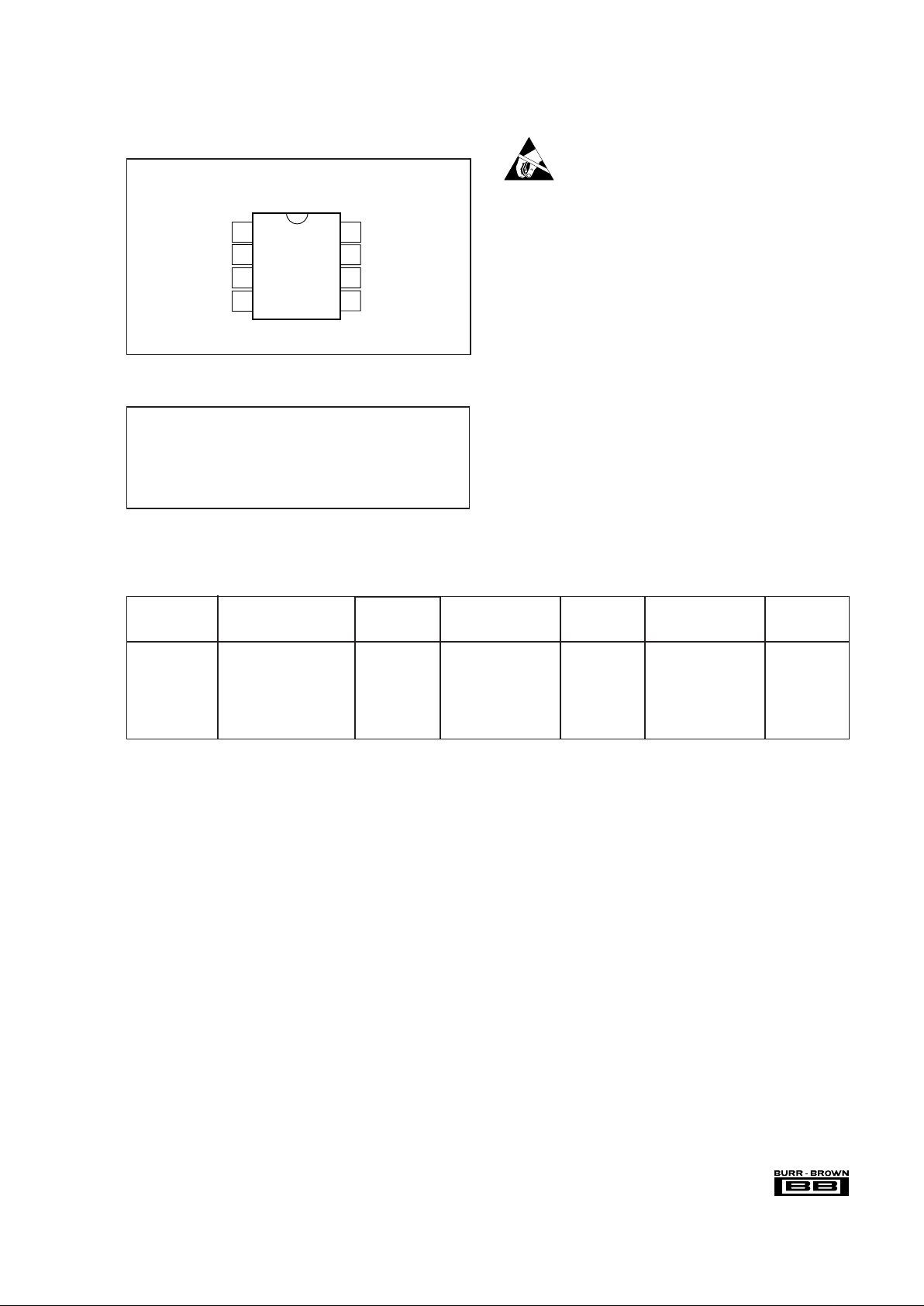
PIN CONFIGURATION
ELECTROSTATIC
DISCHARGE SENSITIVITY
This integrated circuit can be damaged by ESD. Burr-Brown
recommends that all integrated circuits be handled with
appropriate precautions. Failure to observe proper handling
and installation procedures can cause damage.
ESD damage can range from subtle performance degradation
to complete device failure. Precision integrated circuits may
be more susceptible to damage because very small parametric
changes could cause the device not to meet its published
specifications.
Supply Voltage .................................................................................. ±18V
Analog Input Voltage Range ............................................................. ±40V
Output Short-Circuit (to ground) .............................................. Continuous
Operating Temperature ................................................. –55°C to +125°C
Storage Temperature ..................................................... –55°C to +125°C
Junction Temperature .................................................................... +150°C
Lead Temperature (soldering, 10s)............................................... +300°C
NOTE: (1) Stresses above these ratings may cause permanent damage.
Exposure to absolute maximum conditions for extended periods may degrade
device reliability.
ABSOLUTE MAXIMUM RATINGS
(1)
The information provided herein is believed to be reliable; however, BURR-BROWN assumes no responsibility for inaccuracies or omissions. BURR-BROWN assumes
no responsibility for the use of this information, and all use of such information shall be entirely at the user’s own risk. Prices and specifications are subject to change
without notice. No patent rights or licenses to any of the circuits described herein are implied or granted to any third party. BURR-BROWN does not authorize or warrant
any BURR-BROWN product for use in life support devices and/or systems.
Top View 8-Pin DIP and SO-8
R
G
V
–
IN
V
+
IN
V–
R
G
V+
V
O
Ref
1
2
3
4
8
7
6
5
Top View
PACKAGE SPECIFIED
DRAWING TEMPERATURE PACKAGE ORDERING TRANSPORT
PRODUCT PACKAGE NUMBER(1) RANGE MARKING NUMBER(2) MEDIA
Single
INA121P 8-Pin DIP 006 –40°C to +85°C INA121P INA121P Rails
INA121PA 8-Pin DIP 006 –40°C to +85°C INA121PA INA121PA Rails
INA121U SO-8 Surface-Mount 182 –40°C to +85°C INA121U INA121U Rails
" " " " " INA121U/2K5 Tape and Reel
INA121UA SO-8 Surface-Mount 182 –40°C to +85°C INA121UA INA121UA Rails
" " " " " INA121UA/2K5 Tape and Reel
NOTES: (1) For detailed drawing and dimension table, please see end of data sheet, or Appendix C of Burr-Brown IC Data Book. (2) Models with a slash (/) are
available only in Tape and Reel in the quantities indicated (e.g., /2K5 indicates 2500 devices per reel). Ordering 2500 pieces of “INA121U/2K5” will get a single
2500-piece Tape and Reel. For detailed Tape and Reel mechanical information, refer to Appendix B of Burr-Brown IC Data Book.
PACKAGE/ORDERING INFORMATION
Page 4
4
®
INA121
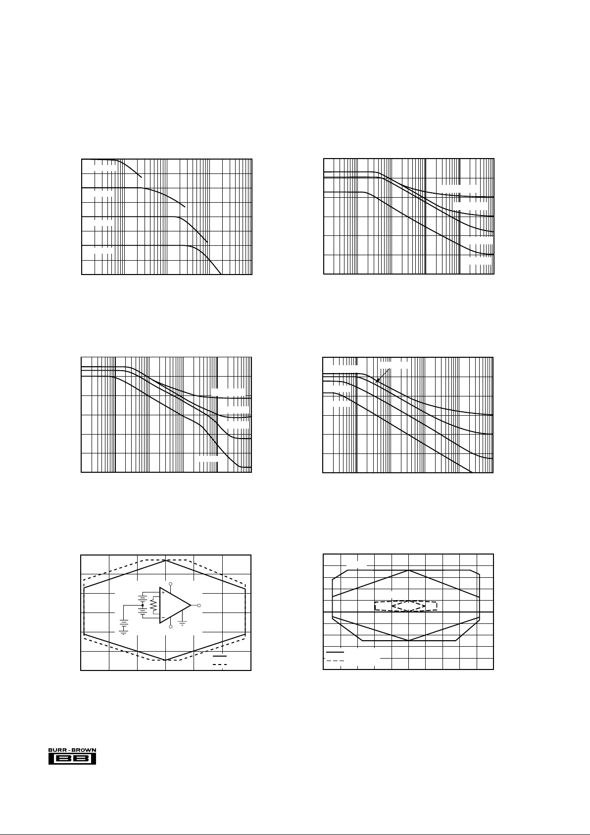
TYPICAL PERFORMANCE CURVES
At TA = +25°C, VS = ±15V, unless otherwise noted.
NEGATIVE POWER SUPPLY REJECTION
vs FREQUENCY
Frequency (Hz)
Power Supply Rejection (dB)
10 100 10k 100k 1M1k
120
100
80
60
40
20
0
G = 1000V/V
G = 1V/V
G = 10V/V
G = 100V/V
INPUT COMMON-MODE RANGE
vs OUTPUT VOLTAGE, V
S
= ±15V
Output Voltage (V)
Common-Mode Voltage (V)
–15 –10 0 5 15–5
15
10
5
0
–5
–10
–15
10
V
D/2
+
–
+
–
+
V
CM
V
O
V
D/2
Ref
–15V
+15V
G = 1
G ≥ 10
POSITIVE POWER SUPPLY REJECTION
vs FREQUENCY
Frequency (Hz)
Power Supply Rejection (dB)
10 100 10k 100k 1M1k
120
100
80
60
40
20
0
G = 1000V/V
G = 1V/V
G = 10V/V
G = 100V/V
COMMON-MODE REJECTION
vs FREQUENCY
Frequency (Hz)
Common-Mode Rejection (dB)
10 100 10k 100k 1M1k
120
100
80
60
40
20
0
G = 1000V/V
G = 1V/V
G = 10V/V
G = 100V/V
INPUT COMMON-MODE RANGE
vs OUTPUT VOLTAGE, V
S
= ±5V, ±2.5V
Output Voltage (V)
Common-Mode Voltage (V)
–5
5
4
3
2
1
0
–1
–2
–3
–4
–5
–4 –3 –2 –1 0 1 2 3 4 5
VS = ±5V
V
S
= ±2.5V
G = 1
G ≥ 10
G = 1
G ≥ 10
GAIN vs FREQUENCY
Frequency (Hz)
Gain (dB)
1k 10k 1M 10M100k
60
50
40
30
20
10
0
–10
–20
G = 1000V/V
G = 100V/V
G = 10V/V
G = 1V/V
Page 5
5
®
INA121
INPUT BIAS CURRENT vs TEMPERATURE
Temperature (°C)
Bias Current (pA)
10k
1k
100
10
1
0.1
0.01
–75 –50 –25 0 25 50 75 100 125
I
B
I
OS
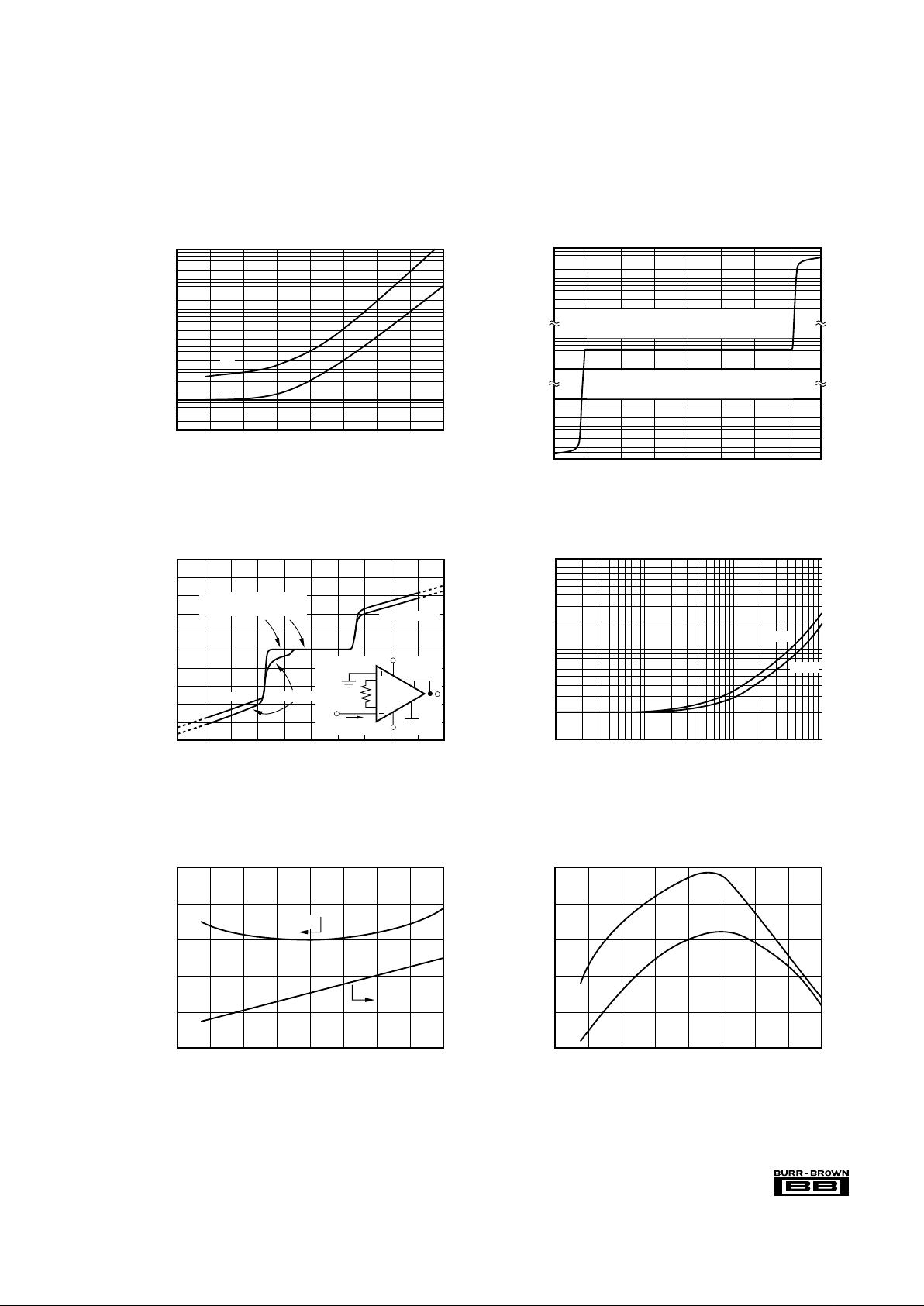
TYPICAL PERFORMANCE CURVES (CONT)
At TA = +25°C, VS = ±15V, unless otherwise noted.
INPUT OVER-VOLTAGE V/I CHARACTERISTICS
1
0.8
0.6
0.4
0.2
0
–0.2
–0.4
–0.6
–0.8
–1
Input Current (mA)
Input Voltage (V)
–50 –40 –30 –20 –10 10 20 30 40050
G = 1V/V
G = 1000V/V
G = 1V/V
Flat region represents
normal linear operation.
V
IN
I
IN
–15V
+15V
G = 1000V/V
QUIESCENT CURRENT AND SLEW RATE
vs TEMPERATURE
500
475
450
425
400
375
–75 –50 –25 0 25 50 75 100 125
Temperature (°C)
Quiescent Current (µA)
1.4
1.2
1
0.8
0.6
0.4
Slew Rate (V/µs)
SR
I
Q
SHORT-CIRCUIT CURRENT
vs TEMPERATURE
±15
±14
±13
±12
±11
±10
–75 –50 –25 0 25 50 75 100 125
Temperature (°C)
Short-Circuit Current (µA)
+I
SC
–I
SC
SETTLING TIME vs GAIN
1000
100
10
1 10 100 1000
Gain (V/V)
Settling Time (µs)
0.01%
0.1%
INPUT BIAS CURRENT
vs COMMON-MODE INPUT VOLTAGE
1m
100µ
10µ
10p
1p
–10µ
–100µ
–1m
–20 –15 –10 –5 0 5 10 15 20
Common-Mode Voltage (V)
Input Bias Current (A)
Page 6
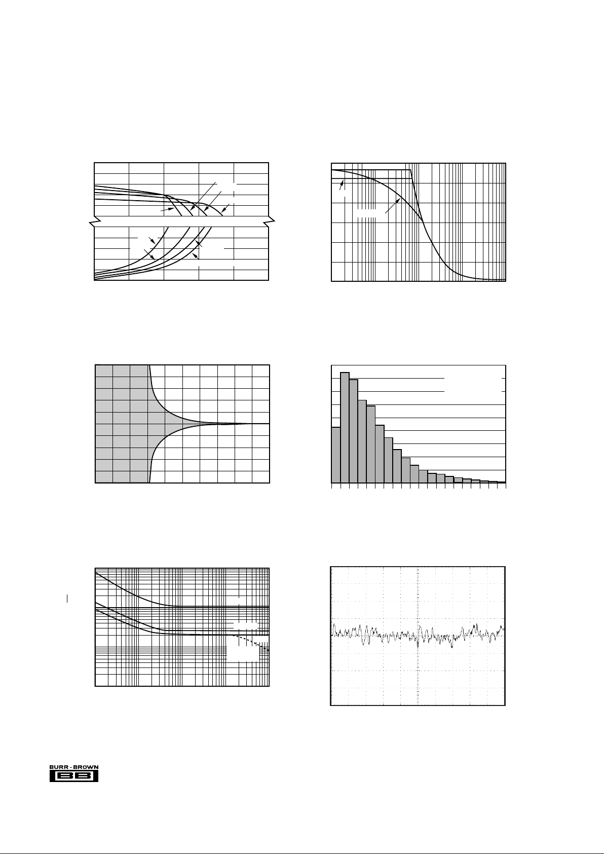
6
®
INA121
TYPICAL PERFORMANCE CURVES (CONT)
At TA = +25°C, VS = ±15V, unless otherwise noted.
0.5µV
VOLTAGE NOISE 0.1 TO 10Hz
INPUT-REFERRED, G ≥ 100
1s/div
OUTPUT VOLTAGE SWING vs OUTPUT CURRENT
V+
(V+) –0.3
(V+) –0.6
(V+) –0.9
(V+) –1.2
(V+) –1.5
(V–) +1.5
(V–) +1.2
(V–) +0.9
(V–) +0.6
(V–) +0.3
(V–)
0 ±2 ±4 ±6 ±8 ±10
Output Current (mA)
Output Voltage Swing (V)
+125°C
+125°C
+85°C
+85°C
–40°C, –55°C
–40°C, –55°C
+25°C
+25°C
INPUT OFFSET VOLTAGE WARM-UP
10
8
6
4
2
0
–2
–4
–6
–8
–10
0
100
200
300
400
500
Time (µs)
Offset Voltage Change (µV)
INPUT OFFSET VOLTAGE DRIFT
PRODUCTION DISTRIBUTION
Percent of Units (%)
Offset Voltage Drift (µV/°C)
18
16
14
12
10
8
6
4
2
0
Typical production
distribution of
packaged units.
0 0.5 1 1.5 2 2.5 3 3.5 4 4.5 5 5.5 6 6.5 7 7.5 8 8.5 9 9.5 10
MAXIMUM OUTPUT VOLTAGE vs FREQUENCY
30
25
20
15
10
5
0
100 1k 10k 100k 1M
Frequency (Hz)
Peak-to-Peak Output Voltage (Vp-p)
G = 1000
G = 10 to 100
G = 1
INPUT-REFERRED NOISE VOLTAGE
vs FREQUENCY
Frequency (Hz)
Voltage Noise (nV/√Hz)
1 10 1k 10k100
1000
100
10
1
G = 1
G = 10
G = 1000
(BW Limit)
G = 100
Page 7
7
®
INA121
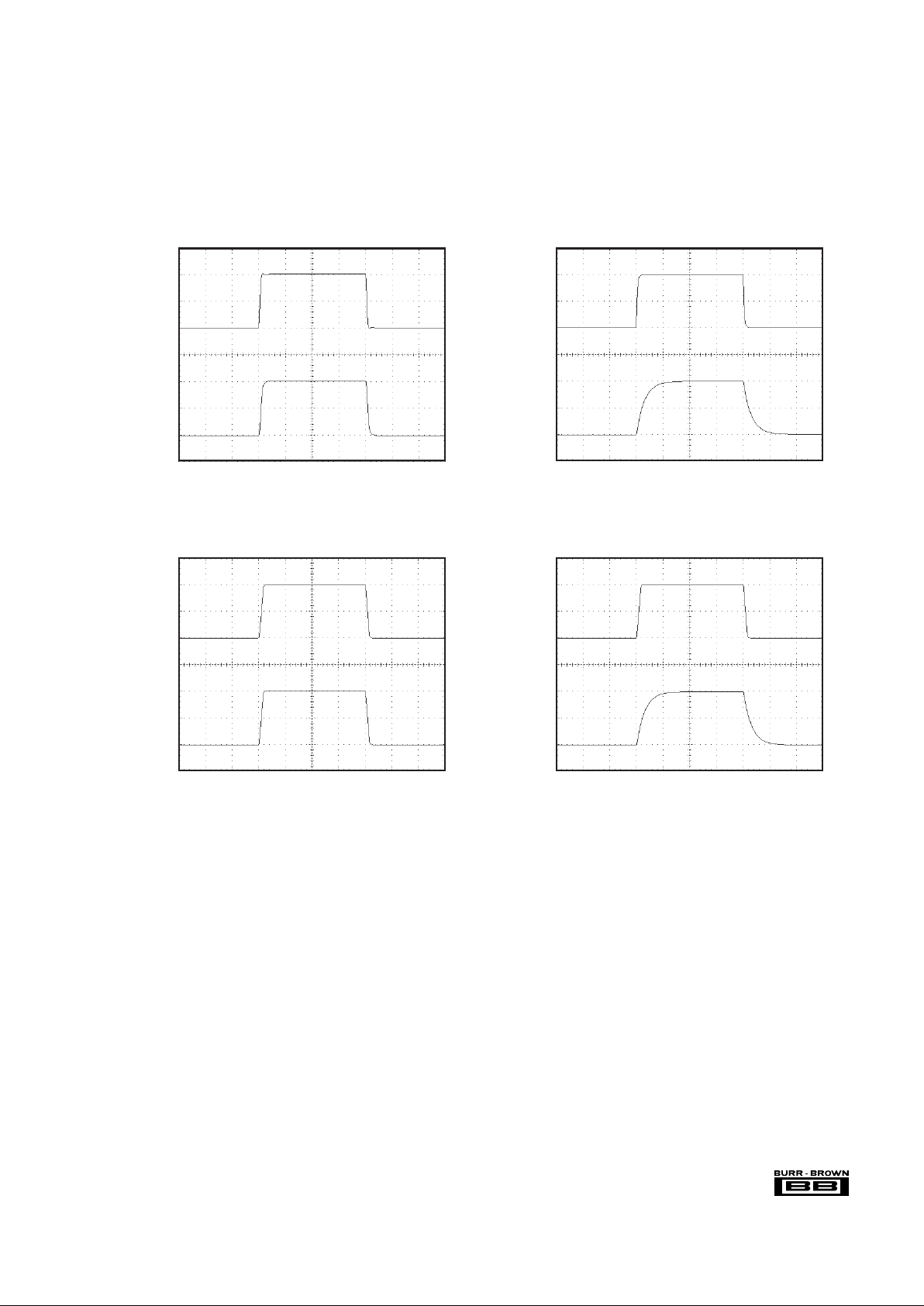
SMALL-SIGNAL STEP RESPONSE
(G = 1, 10)
TYPICAL PERFORMANCE CURVES (CONT)
At TA = +25°C, VS = ±15V, unless otherwise noted.
SMALL-SIGNAL STEP RESPONSE
(G = 100, 1000)
LARGE-SIGNAL STEP RESPONSE
(G = 1, 10)
LARGE-SIGNAL STEP RESPONSE
(G = 100, 1000)
10µs/div
G = 10
50mV/div
G = 1
100µs/div
G = 100
50mV/div
G = 1000
100µs/div
G = 10
5V/div
G = 1
G = 1000
5V/div
G = 100
100µs/div
Page 8
8
®
INA121
APPLICATION INFORMATION
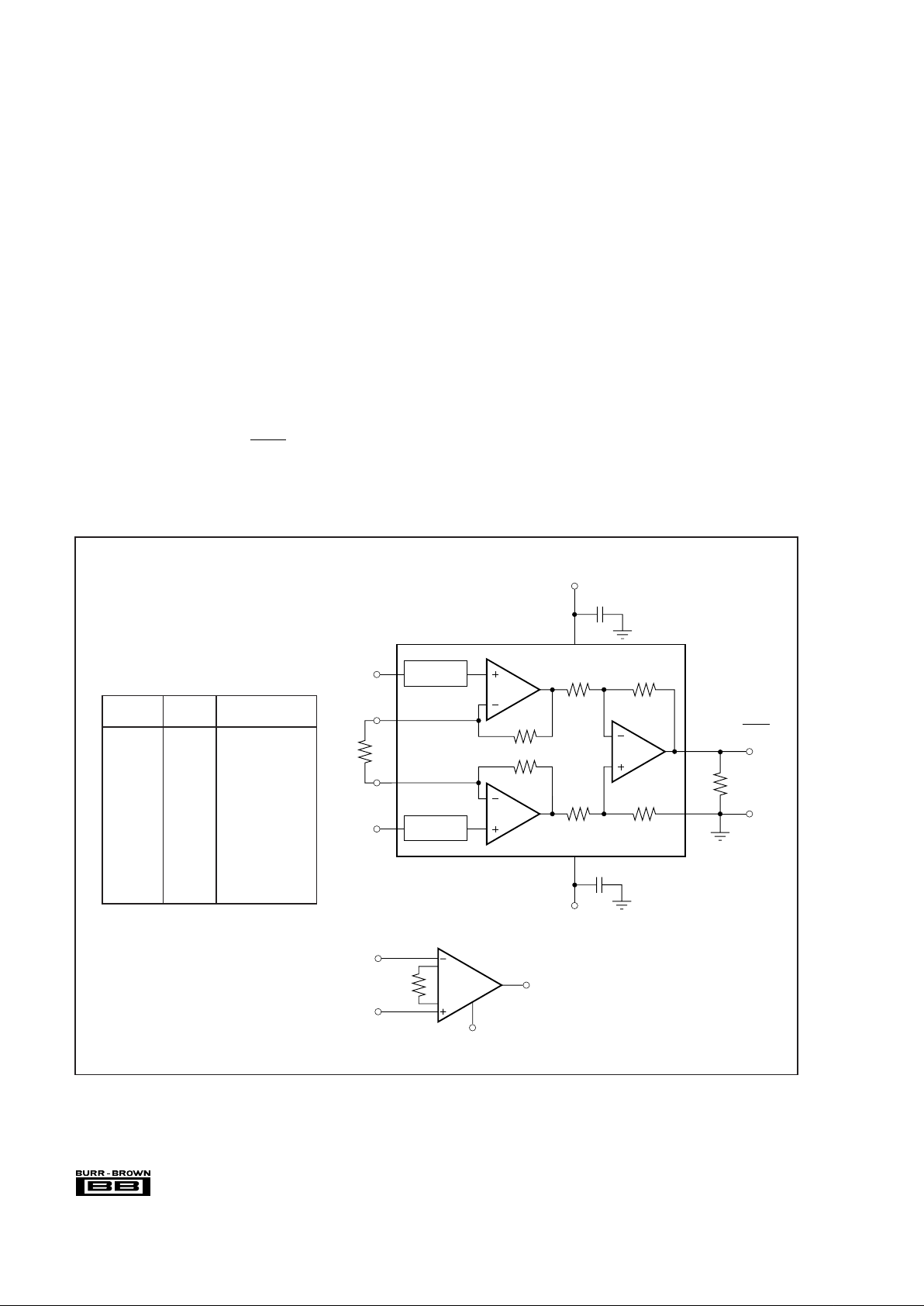
Figure 1 shows the basic connections required for operation
of the INA121. Applications with noisy or high impedance
power supplies may require decoupling capacitors close to
the device pins as shown.
The output is referred to the output reference (Ref) terminal
which is normally grounded. This must be a low-impedance
connection to assure good common-mode rejection. A resistance of 8Ω in series with the Ref pin will cause a typical
device to degrade to approximately 80dB CMR (G = 1).
SETTING THE GAIN
Gain of the INA121 is set by connecting a single external
resistor, R
G
, connected between pins 1 and 8:
Commonly used gains and resistor values are shown in
Figure 1.
(1)
G = 1+
50 kΩ
R
G
The 50kΩ term in Equation 1 comes from the sum of the two
internal feedback resistors of A
1
and A2. These on-chip
metal film resistors are laser trimmed to accurate absolute
values. The accuracy and temperature coefficient of these
resistors are included in the gain accuracy and drift specifications of the INA121.
The stability and temperature drift of the external gain
setting resistor, R
G
, also affects gain. RG’s contribution to
gain accuracy and drift can be directly inferred from the gain
equation (1). Low resistor values required for high gain can
make wiring resistance important. Sockets add to the wiring
resistance which will contribute additional gain error (possibly an unstable gain error) in gains of approximately 100 or
greater.
DYNAMIC PERFORMANCE
The typical performance curve “Gain vs Frequency” shows
that, despite its low quiescent current, the INA121 achieves
wide bandwidth, even at high gain. This is due to the
current-feedback topology of the INA121. Settling time also
remains excellent at high gain.
A
1
A
2
A
3
6
40kΩ40kΩ
40kΩ40kΩ
7
4
3
8
1
2
V
IN
V
IN
R
G
V+
V–
INA121
G = 1 +
50kΩ
R
G
–
+
5
Over-Voltage
Protection
25kΩ
25kΩ
Over-Voltage
Protection
Load
V
O
= G • (VIN – VIN)
+
–
0.1µF
0.1µF
+
–
V
O
R
G
Also drawn in simplified form:
INA121
Ref
V
O
V
IN
–
V
IN
+
Ref
DESIRED R
G
NEAREST 1% R
G
GAIN (Ω )(Ω)
1NC NC
2 50.00k 49.9k
5 12.50k 12.4k
10 5.556k 5.62k
20 2.632k 2.61k
50 1.02k 1.02k
100 505.1 511
200 251.3 249
500 100.2 100
1000 50.05 49.9
2000 25.01 24.9
5000 10.00 10
10000 5.001 4.99
NC: No Connection.
FIGURE 1. Basic Connections.
Page 9
9
®
INA121
INA121
1MΩ1MΩ
INA121
10kΩ
Thermocouple
INA121
Center-tap provides
bias current return.
INA121
Bridge resistance provides
bias current return.
Crystal or
Ceramic
Transducer
BridgeV
REF
The INA121 provides excellent rejection of high frequency
common-mode signals. The typical performance curve,
“Common-Mode Rejection vs Frequency” shows this be-
havior. If the inputs are not properly balanced, however,
common-mode signals can be converted to differential sig-
nals. Run the V
IN
and V
IN
connections directly adjacent each
other, from the source signal all the way to the input pins. If
possible use a ground plane under both input traces. Avoid
running other potentially noisy lines near the inputs.
NOISE AND ACCURACY PERFORMANCE
The INA121’s FET input circuitry provides low input bias
current and high speed. It achieves lower noise and higher
accuracy with high impedance sources. With source impedances of 2kΩ to 50kΩ the INA114, INA128, or INA129 may
provide lower offset voltage and drift. For very low source
impedance (≤1kΩ), the INA103 may provide improved
accuracy and lower noise. At very high source impedances
(> 1MΩ) the INA116 is recommended.
OFFSET TRIMMING
The INA121 is laser trimmed for low offset voltage and
drift. Most applications require no external offset adjustment. Figure 2 shows an optional circuit for trimming the
output offset voltage. The voltage applied to Ref terminal is
summed at the output. The op amp buffer provides low
impedance at the Ref terminal to preserve good commonmode rejection. Trim circuits with higher source impedance
should be buffered with an op amp follower circuit to assure
low impedance on the Ref pin.
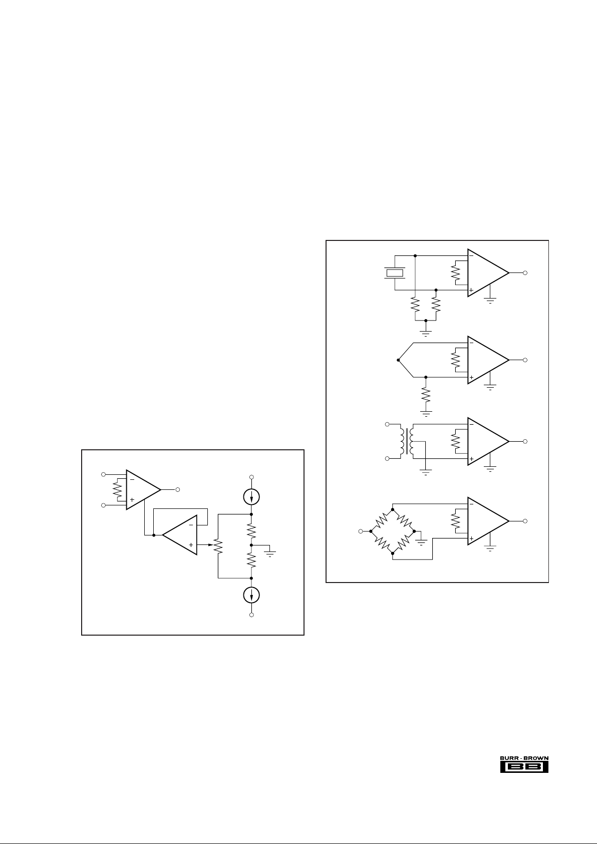
Input circuitry must provide a path for this input bias current
if the INA121 is to operate properly. Figure 3 shows various
provisions for an input bias current path. Without a bias
current return path, the inputs will float to a potential which
exceeds the common-mode range of the INA121 and the
input amplifiers will saturate.
If the differential source resistance is low, the bias current
return path can be connected to one input (see the thermocouple example in Figure 3). With higher source impedance,
using two resistors provides a balanced input with possible
advantages of lower input offset voltage due to bias current
and better high-frequency common-mode rejection.
+
–
INPUT BIAS CURRENT RETURN PATH
The input impedance of the INA121 is extremely high—
approximately 10
12
Ω. However, a path must be provided for
the input bias current of both inputs. This input bias current
is typically 4pA. High input impedance means that this input
bias current changes very little with varying input voltage.
INA121
V
IN
V
IN
R
G
–
+
10kΩ
(1)
V
O
OPA277
Ref
±10mV
Adjustment Range
100Ω
(1)
100Ω
(1)
100µA
1/2 REF200
100µA
1/2 REF200
V+
V–
NOTE: (1) For wider trim range required
in high gains, scale resistor values larger
INPUT COMMON-MODE RANGE
The linear input voltage range of the input circuitry of the
INA121 is from approximately 1.2V below the positive
supply voltage to 2.1V above the negative supply. A differential input voltage causes the output voltage to increase.
The linear input range, however, will be limited by the
output voltage swing of amplifiers A
1
and A2. So the linear
common-mode input range is related to the output voltage of
the complete amplifier. This behavior also depends on supply voltage—see typical performance curve “Input Common-Mode Range vs Output Voltage”.
FIGURE 3. Providing an Input Common-Mode Current Path.
FIGURE 2. Optional Trimming of Output Offset Voltage.
Page 10
10
®
INA121
INA121
R
G
100Ω
V
O
+10V
Bridge
G = 500
Ref
A
1
A
2
A
3
40kΩ40kΩ
40kΩ40kΩ
R
G
V+
V–
INA121
V
O
= G • V
D
G = 1 +
50kΩ
R
G
25kΩ
25kΩ
VCM –
G • V
D
2
V
D
2
V
D
2
V
CM
VCM +
G • V
D
2
A combination of common-mode and differential input
voltage can cause the output of A
1
or A2 to saturate. Figure
4 shows the output voltage swing of A
1
and A2 expressed in
terms of a common-mode and differential input voltages.
For applications where input common-mode range must be
maximized, limit the output voltage swing by connecting the
INA121 in a lower gain (see performance curve “Input
Common-Mode Voltage Range vs Output Voltage”). If
necessary, add gain after the INA121 to increase the voltage
swing.
Input-overload can produce an output voltage that appears
normal. For example, if an input overload condition drives
both input amplifiers to their positive output swing limit, the
difference voltage measured by the output amplifier will be
near zero. The output of A
3
will be near 0V even though both
inputs are overloaded.
LOW VOLTAGE OPERATION
The INA121 can be operated on power supplies as low as
±2.25V. Performance remains excellent with power supplies
ranging from ±2.25V to ±18V. Most parameters vary only
slightly throughout this supply voltage range—see typical
performance curves. Operation at very low supply voltage
requires careful attention to assure that the input voltages
remain within their linear range. Voltage swing requirements
of internal nodes limit the input common-mode range with low
power supply voltage. Typical performance curves, “Input
Common-Mode Range vs Output Voltage” show the range of
linear operation for ±15V, ±5V, and ±2.5V supplies.
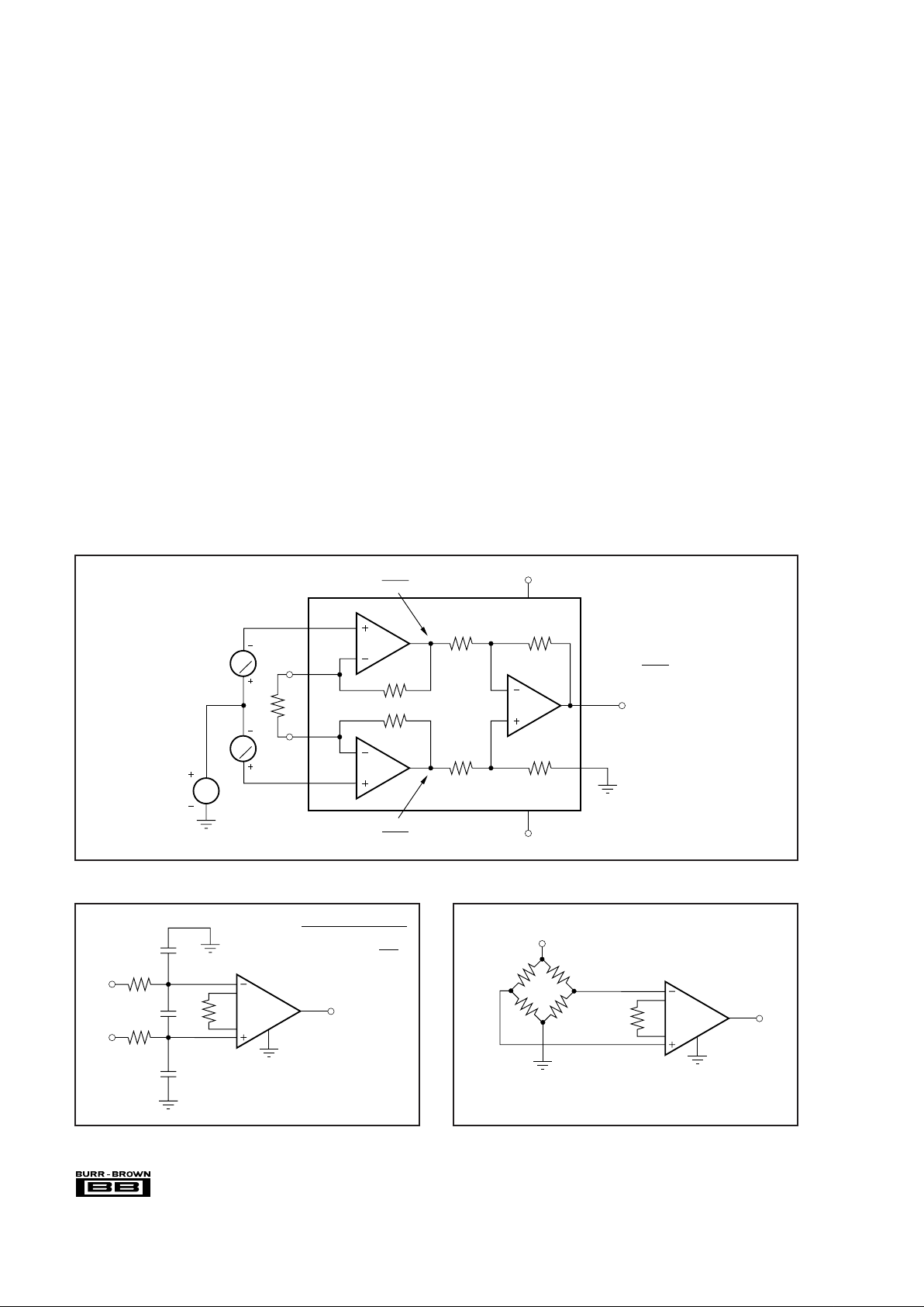
INPUT FILTERING
The INA121’s FET input allows use of an R/C input filter
without creating large offsets due to input bias current.
Figure 5 shows proper implementation of this input filter to
preserve the INA121’s excellent high frequency commonmode rejection. Mismatch of the common-mode input time
constant (R
1C1
and R2C2), either from stray capacitance or
mismatched values, causes a high frequency common-mode
signal to be converted to a differential signal. This degrades
common-mode rejection. The differential input capacitor,
C3, reduces the bandwidth and mitigates the effects of
mismatch in C
1
and C2. Make C3 much larger than C1 and
C
2
. If properly matched, C1 and C2 also improve ac CMR.
FIGURE 4. Voltage Swing of A1 and A2.
FIGURE 5. Input Low-Pass Filter.
FIGURE 6. Bridge Transducer Amplifier.
f
−3dB
=
1
4πR
1C3
+
C
1
2
INA121
V
O
V
IN
–
V
IN
+
R
1
R
2
C
3
C
1
C2R1 = R
2
C1 = C
2
C3 ≈ 10C
1
FET input allows use
of large resistors and
small capacitors.
Ref
Page 11
11
®
INA121
INA121
Transducer
C
1
C
2
Null
R
2
R
1
R
G
V
O
Ref
V
AC
INA121
OPA277
C
1
50nF
R
G
R
2
R
G
Make G ≤ 10 where G = 1 +
50k
Load
V
IN
G • R
2
IL =
R
1
10kΩ
V
IN
Ref
INA121
R
G
V
O
C
1
0.1µF
OPA277
Ref
R
1
1MΩ
f
–3dB
=
1
2πR
1C1
= 1.59Hz
V
IN
+
–
INA121 ISO124
±6V to ±18V
Isolated Power
±15V
Ref
V
IN
–
V
IN
+
V
O
Isolated
Common
V+ V–
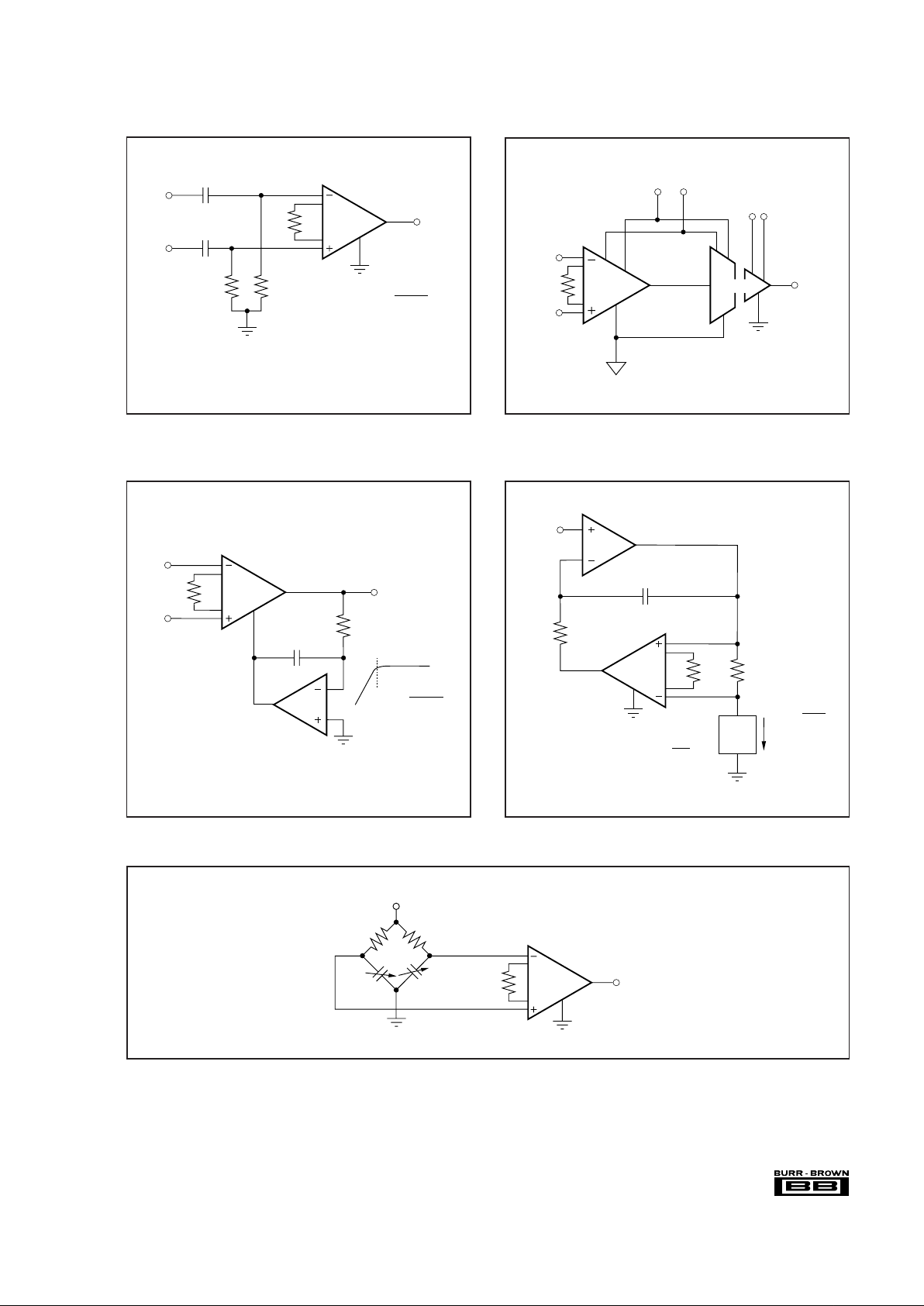
FIGURE 8. Galvanically Isolated Instrumentation
Amplifier.
FIGURE 7. High-Pass Input Filter.
FIGURE 10. Voltage Controlled Current Source.FIGURE 9. AC-Coupled Instrumentation Amplifier.
INA121
C
1
C
2
R
1
R
2
V
O
2πR1C
1
1
f
c
=
NOTE: To preserve good low frequency CMR,
make R
1
= R2 and C1 = C2.
R
G
Ref
FIGURE 11. Capacitive Bridge Transducer Circuit.
Page 12
12
®
INA121
INA121
R
G
/2
R
G
= 5.6kΩ
V
O
LA
RL
RA
10kΩ
Ref
NOTE: Due to the INA121’s current-feedback
topology, V
G
is approximately 0.7V less than
the common-mode input voltage. This DC offset
in this guard potential is satisfactory for many
guarding applications.
Low bias current
allows use with high
electrode impedances.
G = 10
2.8kΩ
V
G
V
G
2.8kΩ
1/2
OPA2131
390kΩ
390kΩ
1/2
OPA2131
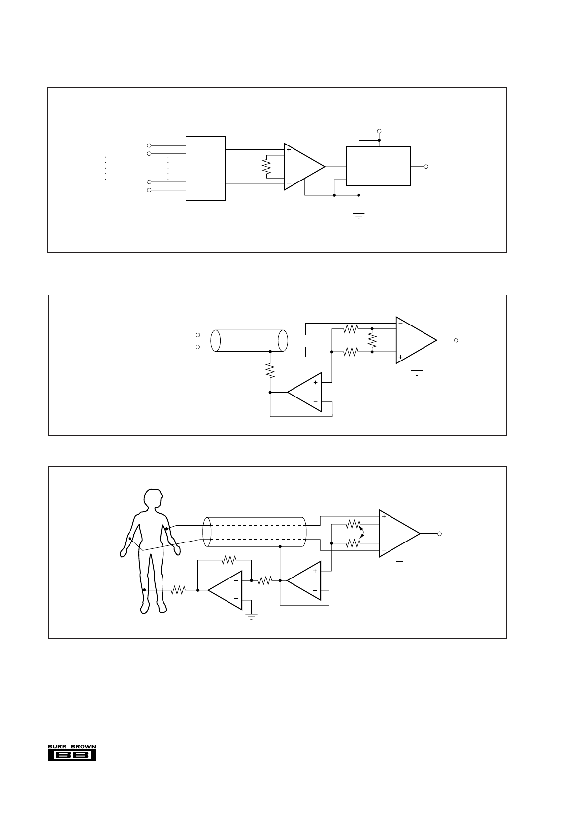
FIGURE 12. Multiplexed-Input Data Acquisition System.
FIGURE 13. Shield Driver Circuit.
INA121
V
IN
–
V
IN
+
OPA130
511Ω
22.1kΩ
22.1kΩ
Ref
V
O
For G = 100
R
G
= 511Ω // 2(22.1kΩ)
effective R
G
= 505Ω
100Ω
NOTE: Driving the shield minimizes CMR degradation
due to unequally distributed capacitance on the input
line. The shield is driven at approximately 1V below
the common-mode input voltage.
FIGURE 14. ECG Amplifier With Right-Leg Drive.
INA121
V
IN
+
–
V
IN
+
–
Channel 8
Channel 1
MPC800
MUX
ADS7816
+5V
V
REF
+In
–In
12 Bits Out
Serial
R
G
Ref
 Loading...