

Page 1
TECHNICAL DATA
432
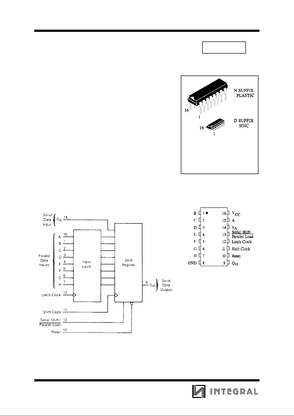
8-Bit Serial or Parallel-Input/
Serial-Output Shift Register
with Input Latch
High-Performance Silicon-Gate CMOS
The IN74HC597 is identical in pinout to the LS/ALS597. The
device inputs are compatible with standard CMOS outputs; with pullup
resistors, they are compatible with LS/ALSTTL outputs.
This device consists of an 8-bit input latch which feeds parallel
data to an 8-bit shift register. Data can also be loaded serially (see
Function Tab l e).
•
Outputs Directly Interface to CMOS, NMOS, and TTL
•
Operating Voltage Range: 2.0 to 6.0 V
•
Low Input Current: 1.0 µA
•
High Noise Immunity Characteristic of CMOS Devices
IN74HC597
ORDERING INFORMATION
IN74HC597N Plastic
IN74HC597D SOIC
TA = -55° to 125° C for all packages
PIN ASSIGNMENT
LOGIC DIAGRAM
PIN 16 =V
CC
PIN 8 = GND
Page 2
IN74HC597
433
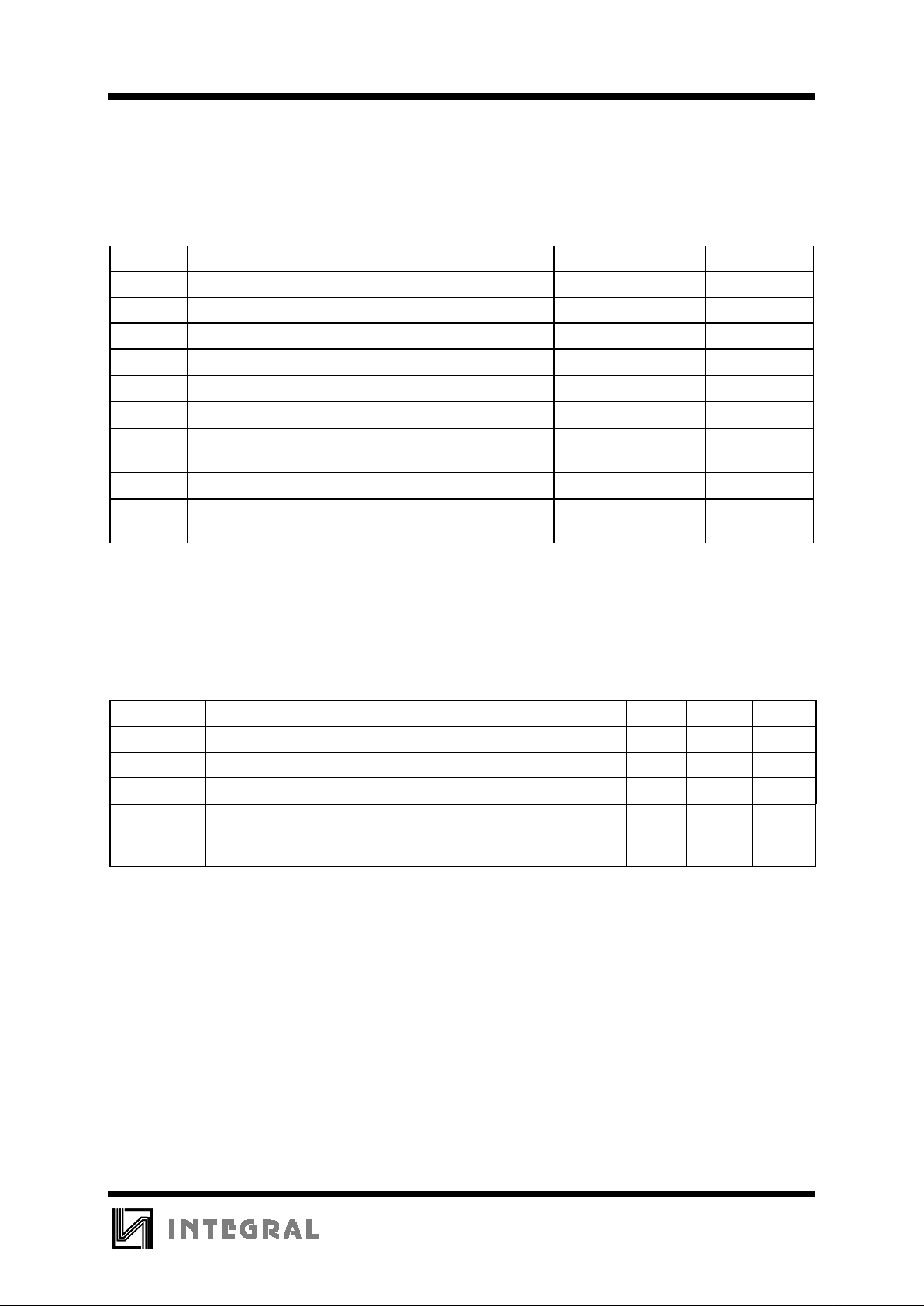
MAXIMUM RATINGS
*
Symbol Parameter Value Unit
V
CC
DC Supply Voltage (Referenced to GND) -0.5 to +7.0 V
V
IN
DC Input Voltage (Referenced to GND) -1.5 to VCC +1.5 V
V
OUT
DC Output Voltage (Referenced to GND) -0.5 to VCC +0.5 V
I
IN
DC Input Current, per Pin
±
20
mA
I
OUT
DC Output Current, per Pin
±
25
mA
I
CC
DC Supply Current, VCC and GND Pins
±
50
mA
P
D
Power Dissipation in Still Air, Plastic DIP+
SOIC Package+
750
500
mW
Tstg Storage Temperature -65 to +150
°
C
T
L
Lead Temperature, 1 mm from Case for 10 Seconds
(Plastic DIP or SOIC Package)
260
°
C
*
Maximum Ratings are those values beyond which damage to the device may occur.
Functional operation should be restricted to the Recommended Operating Conditions.
+Derating - Plastic DIP: - 10 mW/°C from 65° to 125°C
SOIC Package: : - 7 mW/°C from 65° to 125°C
RECOMMENDED OPERATING CONDITIONS
Symbol Parameter Min Max Unit
V
CC
DC Supply Voltage (Referenced to GND) 2.0 6.0 V
VIN, V
OUT
DC Input Voltage, Output Voltage (Referenced to GND) 0 V
CC
V
T
A
Operating Temperature, All Package Types -55 +125
°
C
tr, t
f
Input Rise and Fall Time (Figure 1) VCC =2.0 V
V
CC
=4.5 V
V
CC
=6.0 V
0
0
0
1000
500
400
ns
This device c ontains p rote ction ci rcuitr y to guard a gainst damage d ue to high st atic voltages or electr ic
fields. However, precautions must be taken to avoid applications of any voltage higher than maximum rated
voltages to this high-impedance circuit. For proper operation, V
IN
and V
OUT
should be constrained to the range
GND≤(V
IN
or V
OUT
)≤VCC.
Unused inputs must always be tied to an appropriate logic voltage level (e.g., either GND or V
CC
).
Unused outputs must be left open.
Page 3
IN74HC597
434
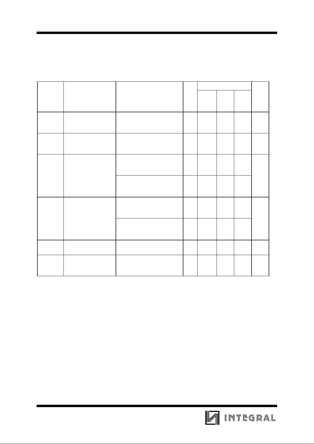
DC ELECTRICAL CHARACTERISTICS
(Voltages Referenced to GND)
V
CC
Guaranteed Limit
Symbol Parameter Test Conditions V
25 °C
to
-55°C
≤
85
°
C
≤
125
°
C
Unit
V
IH
Minimum High-Level
Input Voltage
V
OUT
=0.1 V or VCC-0.1 V
I
OUT
≤
20 µA
2.0
4.5
6.0
1.5
3.15
4.2
1.5
3.15
4.2
1.5
3.15
4.2
V
V
IL
Maximum Low Level Input Voltage
V
OUT
=0.1 V or VCC-0.1 V
I
OUT
≤
20 µA
2.0
4.5
6.0
0.3
0.9
1.2
0.3
0.9
1.2
0.3
0.9
1.2
V
V
OH
Minimum High-Level
Output Voltage
VIN=VIH or V
IL
I
OUT
≤
20 µA
2.0
4.5
6.0
1.9
4.4
5.9
1.9
4.4
5.9
1.9
4.4
5.9
V
VIN=VIH or V
IL
I
OUT
≤
4.0 mA
I
OUT
≤
5.2 mA
4.5
6.0
3.98
5.48
3.84
5.34
3.7
5.2
V
OL
Maximum Low-Leve l
Output Voltage
VIN=VIH or V
IL
I
OUT
≤
20 µA
2.0
4.5
6.0
0.1
0.1
0.1
0.1
0.1
0.1
0.1
0.1
0.1
V
VIN=VIH or V
IL
I
OUT
≤
4.0 mA
I
OUT
≤
5.2 mA
4.5
6.0
0.26
0.26
0.33
0.33
0.4
0.4
I
IN
Maximum Input
Leakage Current
VIN=VCC or GND 6.0
±
0.1
±
1.0
±
1.0
µ
A
I
CC
Maximum Quiesce nt
Supply Current
(per Package)
VIN=VCC or GND
I
OUT
=0µA
6.0 8.0 80 160
µ
A
Page 4

IN74HC597
435
AC ELECTRICAL CHARACTERISTICS
(CL=50pF,Input tr=tf=6.0 ns)
V
CC
Guaranteed Limit
Symbol Parameter V
25 °C
to
-55°C
≤85°C≤
125°C
Unit
f
max
Minimum Clock Frequency (50 % D ut y Cycle)
(Figures 2 and 8)
2.0
4.5
6.0
6.0
30
35
4.8
24
28
4.0
20
24
MHz
t
PLH
, t
PHL
Maximum Propagat ion Delay, Latch Clock to Q
H
(Figures 1 and 8)
2.0
4.5
6.0
210
42
36
265
53
45
315
63
54
ns
t
PLH
, t
PHL
Maximum Propagation Delay , Shift Clock to Q
H
(Figures 2 and 8)
2.0
4.5
6.0
175
35
30
220
44
37
265
53
45
ns
t
PHL
Maximum Propagation Delay , Reset to Q
H
(Figures 3 and 8)
2.0
4.5
6.0
175
35
30
220
44
37
265
53
45
ns
t
PLH
, t
PHL
Maximum Propagation Delay, Serial Shift/
Parallel Load to Q
H
(Figures 4 and 8)
2.0
4.5
6.0
175
35
30
220
44
37
265
53
45
ns
t
TLH
, t
THL
Maximum Output Transition Time, Any Output
(Figures 1 and 8)
2.0
4.5
6.0
75
15
13
95
19
16
110
22
19
ns
C
IN
Maximum Input Capacitance - 10 10 10 pF
Power Dissipation Capacitance (Per Package)
Typical @25°C,V
CC
=5.0 V
C
PD
Used to determine the no-load dynamic power
consumption:
P
D=CPDVCC
2
f+ICCV
CC
50 pF
Page 5

IN74HC597
436
TIMING REQUIREMENTS
(CL=50pF,Input tr=tf=6.0 ns)
V
CC
Guaranteed Limit
Symbol Parameter V
25 °C to
-55°C
≤85°
C
≤
125°C
Unit
t
su
Minimum Setup Time, Parallel Data
Inputs A-H to Latch Clock
(Figure 5)
2.0
4.5
6.0
100
20
17
125
25
21
150
30
26
ns
t
su
Minimum Setup Time, S erial Data
Input S
A
to Shift Clock (Figure 6)
2.0
4.5
6.0
100
20
17
125
25
21
150
30
26
ns
t
su
Minimum Setup Time, S erial
Shift/Parallel Load to Shift Clock
(Figure 7)
2.0
4.5
6.0
100
20
17
125
25
21
150
30
26
ns
t
h
Minimum Hold Time, Latch Clock to
Parallel Data Inputs A-H
(Figure 5)
2.0
4.5
6.0
25
5
5
30
6
6
40
8
7
ns
t
h
Minimum Hold Time, Shift Clock to
Serial Data Input S
A
(Figure 6)
2.0
4.5
6.0
5
5
5
5
5
5
5
5
5
ns
t
rec
Minimum Recovery Time, Reset
Inactive to Shift Clock (Figure 3)
2.0
4.5
6.0
100
20
17
125
25
21
150
30
26
ns
t
w
Minimum Pulse Width, Latch Clock
and Shift Clock (Figures 1 and 2)
2.0
4.5
6.0
80
16
14
100
20
17
120
24
20
ns
t
w
Minimum Pulse Width, Reset (Figure3)2.0
4.5
6.0
80
16
14
100
20
17
120
24
20
ns
t
w
Minimum Pul se Width, Serial
Shift/Parallel Load (Figure 4)
2.0
4.5
6.0
80
16
14
100
20
17
120
24
20
ns
tr, t
f
Maximum Input Rise and Fal l Times
(Figure 1)
2.0
4.5
6.0
1000
500
400
1000
500
400
1000
500
400
ns
Page 6

IN74HC597
437
FUNCTION TABLE
Inputs Resulting Function
Operation Reset S e r i a l S h i f t/
Parallel Load
Latch
Clock
Shift
Clock
Serial
Input
S
A
Parallel
Inputs
A-H
Latch
Contents
Shift
Register
Contents
Output Q
H
Reset shift register L X L,H, X X X U L L
Reset shift register;
load parallel data
into data latch
LX XXa-ha-h L L
Load parallel data
into data latch
HH L,H,Xa-ha-h U U
Transfer latch
contents to shift
register
H L L,H, X X X U LRN SR
N
LR
H
Contents of data
latch and shift
register are
unchanged
H H L,H, L,H, X X U U U
Load parallel data
into data latch and
shift register
H L X X a-h a-h a-h h
Shift serial data into
shift register
HH X DX *SR
A
=D;
SR
N
SR
N+1
SRG SR
H
Load parallel data
into data latch and
shift serial data into
shift register
HH Da-ha-hSR
A
=D;
SR
N
SR
N+1
SRG SR
H
SR = shift register contents X = don’t care
LR = latch register contents a-h = data at parallel data inputs A-H
D = data (L,H) at serial data input S
A
* = depends on Latch Clock input
U = remains unchanged
INPUTS:
A, B, C, D, E, F, G, H
- Parallel data inputs. Data on
these inputs is stored in the input latch on the rising
edge of the Latch Clock input.
S
A
- Serial data input. Data on this input is shifted into
the shift register on the rising edge of the Shift Clock
input if Serial Shift/Parallel Load is high. Data on this
input is ignored when Serial Shift/
Parallel Load is low.
SERIAL SHIFT/PARALLEL LOAD
- Shift register
mode control. When a high level is applied to this pin,
the shift register is allowed to serially shift data. When
a low level is applied to this pin, the shift register
accepts parallel data from the input latch, and serial
shifting is inhibited.
RESET
- Asynchronous, Active-low shift register
reset. A low level applied to this input resets the shift
register to a low level, but does not change the data in
the input latch.
SHIFT CLOCK
- Serial shift register clock. A lowto-high transition on this input shifts data on the Serial
Data Input into the shift register and data in stage H is
shifted out Q
H
, being replaced by the data previously
stored in stage G.
LATCH CLOCK -
A low-to-high transition on this
input loads the parallel data on inputs A-H into the
input latch.
OUTPUT:
Q
H
- Serial data output. This pin is the output from the
last stage of the shift register.
Page 7

IN74HC597
438
Figure 1. (Serial Shift/Parallel Load = L) Figure 2. (Serial Shift/Parallel Load = H)
Figure 3. Switching Waveforms Figure 4. Switching Waveforms
Figure 5. Switching Waveforms Figure 6. Switching Waveforms
Figure 7. Test Circuit Figure 8. Test Circuit
Page 8

IN74HC597
439
TIMING DIAGRAM
Page 9

IN74HC597
440
EXPANDED LOGIC DIAGRAM
 Loading...