

Page 1

TECHNICAL DATA
1
Octal 3-State Noninverting D Flip-Flop
The device is comprised of eight edge-triggered D-Type flip-flops.
On the positive transition of the clock, the Q outputs will be set to the
logic states that were set up at the D inputs.
A buffered output control input can be used to place the eight
outputs in either a normal logic state (high or low logic levels) or a
high-impedance state. In the high-impedance state the outputs neither
load nor drive the bus lines significantly.
•
Switching specificatio ns at 50 pF
•
Switching specifications guaranteed over full temperature and V
CC
range
•
TRI-STATE buffer-type outputs drive bus lines directly
IN74ALS574
ORDERING INFORMATION
IN74ALS574N Plastic
IN74ALS574DW SOIC
TA = -10° to 70° C
for all packages
FUNCTION TABLE
Inputs Output
Output
Enable
Clock D Q
LHH
LLL
LL,H, X no
change
HXXZ
X = don’t care
Z = high impedance
LOGIC DIAGRAM
PIN 20=V
CC
PIN 10 = GND
PIN ASSIGNMENT
Page 2

IN74ALS574
2
MAXIMUM RATINGS
*
Symbol Parameter Value Unit
V
CC
Supply Voltage 7.0 V
V
IN
Input Voltage 7.0 V
V
OUT
Output Voltage (Referenced to GND) 5.5 V
Tstg Storage Temperature Range -65 to +150
°
C
*
Maximum Ratings are those values beyond which damage to the device may occur.
Functional operation should be restricted to the Recommended Operating Conditions.
RECOMMENDED OPERATING CONDITIONS
Symbol Parameter Min Max Unit
V
CC
Supply Voltage 4.5 5.5 V
V
IH
High Level Input Voltage 2.0 V
V
IL
Low Level Input Voltage 0.8 V
I
OH
High Level Output Current -2.6 mA
I
OL
Low Level Output Current 24 mA
T
A
Ambient Temperature Range -10 +70
°
C
DC ELECTRICAL CHARACTERISTICS
over full operating conditions
Guaranteed Limit
Symbol Parameter Test Conditions Min Max Unit
V
IK
Input Clamp Voltage VCC = min, IIN = -18 mA -1.5 V
V
OH
High Level Output Voltage VCC = min, IOH = -0.4 mA 2.5 V
VCC = min, IOH = -2.6 mA 2.4
V
OL
Low Level Output Voltage VCC = min, IOL = 12 mA 0.4 V
VCC = min, IOL = 24 mA 0.5
I
OZH
Output Off Current HIGH VCC = max, V
OUT
= 2.7 V 20
µ
A
I
OZL
Output Off Current LOW VCC = max, V
OUT
= 0.4 V -20
µ
A
I
IH
High Level Input Current VCC = max, VIN = 2.7 V 20
µ
A
VCC = max, VIN = 7.0 V 0.1 mA
I
IL
Low Level Input Current VCC = max, VIN = 0.4 V -0.1 mA
I
O
Output Short Circuit Current VCC = max, VO = 2.25 V -30 -112 mA
I
CC
Supply Current VCC = max Outputs Low 17 mA
Outputs High 24
3-State
(High Z)
27
Page 3

IN74ALS574
3
AC ELECTRICAL CHARACTERISTICS
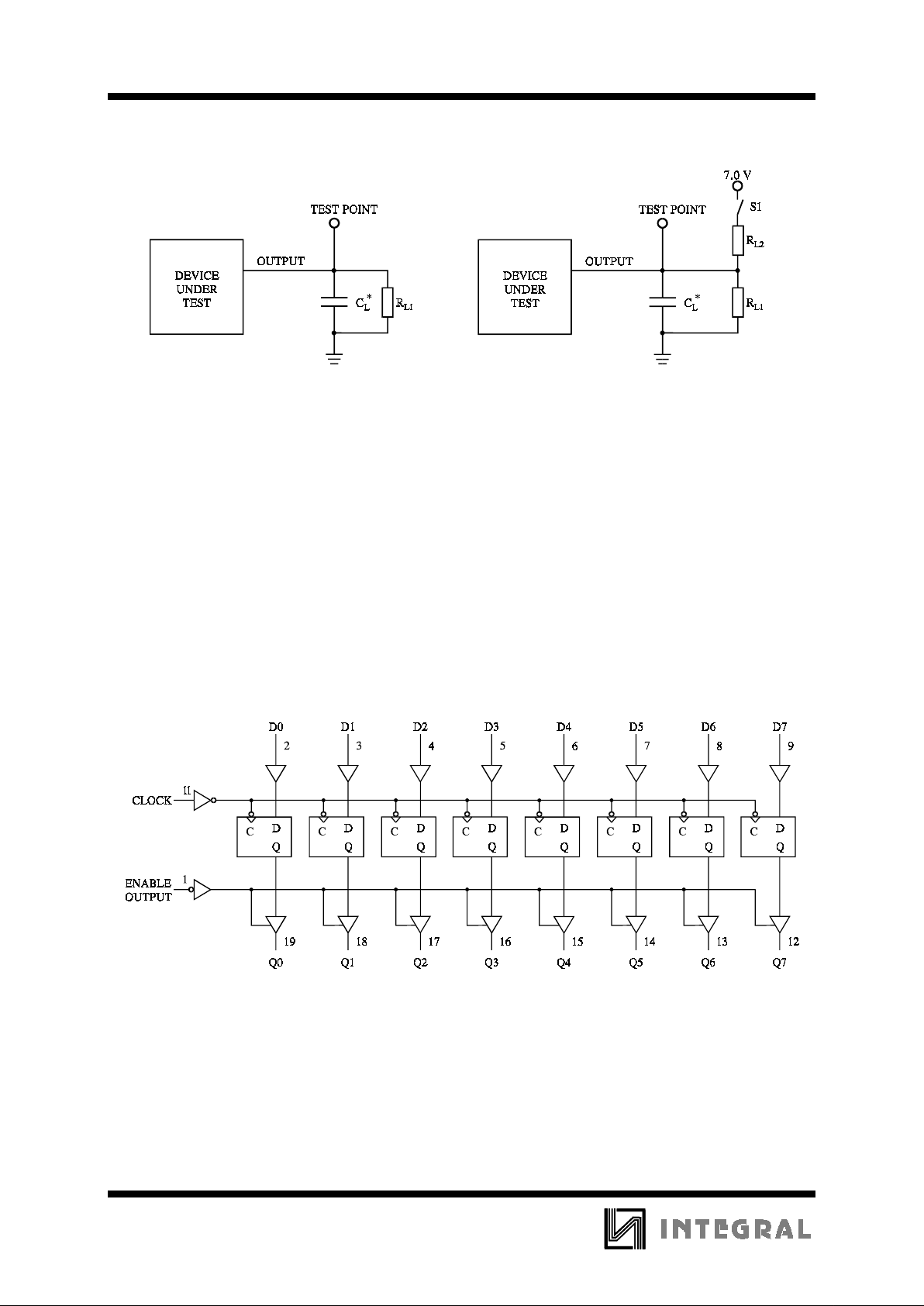
over full operating conditions
(VCC = 5.0 V±10%, CL = 50 pF, RL1 = RL2 = 500 Ω, Input tr = tf = 2.0 ns)
Guaranteed Limit
Symbol Parameter Min Max Unit
f
max
Maximum Clock Frequency 35 MHz
t
PLH
, t
PHL
Propagation Delay Time, from Clock to Output 14 ns
t
PZH
, t
PZL
Propagation Delay Time, from Enable to Any Q 18 ns
t
PHZ
Propagation Delay Time, from Enable to Any Q 32 ns
t
PLZ
Propagation Delay Time, from Enable to Any Q 18 ns
t
w
Pulse Duratio, Enable, 25°C at 5.0 V
16.5 ns
t
su
Data Setup Time before Clock 15 ns
t
h
Data Hold Time after Clock 4 ns
t
PZL
, t
PLZ
- S1 closed
t
PZH
, t
PHZ
- S1 opened
Figure 1. Switching Waveforms Figure 2. Switching Waveforms
Figure 3. Switching Waveforms
Page 4
IN74ALS574
4
* Includes all probe and jig capacitance. * Includes all probe and jig capacitance.
Figure 3. Test Circuit Figure 4. Test Circuit
EXPANDED LOGIC DIAGRAM
 Loading...