

Datasheet IMSC011-P20S, IMSC011-E20S, IMSC011-W20S Datasheet (SGS Thomson Microelectronics)
Page 1
)
FEATURES
Standard INMOS link protocol
10 or 20 Mbits/sec operating speed
Communicates with transputers
IMS C011
Link adaptor
Converts between serial link and parallel bus
Converts between serial link and parallel device
Two modes of parallel operation:
Mode 1: Peripheral interface
Eight bitparallel input interface
Eight bitparallel output interface
Full handshake on input and output
Mode 2: Bus interface
Tristatebidirectional bus interface
Memory mapped registers
Interrupt capability
Single +5V 5% power supply
TTL and CMOS compatibility
120mW power dissipation
28 pin 0.6” plastic package
28 pin SOJ package
28 pin LCCC package
Extended temperature version available
System
Services
Link
System
Services
Mode 1
Input
Interface
Output
Interface
Interrupt
Control
Register
Select
8
8
APPLICATIONS
Programmable I/O for transputer
Connecting microprocessors to transputers
High speed links between microprocessors
Inter-family microprocessor interfacing
Interconnecting different speed links
Link
Mode 2
Data and
Status
Registers
8
July 1995
42 1412 08
1/30
Page 2

Contents
1 Introduction 3......................................................
2 Pin designations 4..................................................
3 System services 5..................................................
3.1 Power 5.....................................................................
3.2 CapMinus 5.................................................................
3.3 ClockIn 5....................................................................
3.4 SeparateIQ 6................................................................
3.5 Reset 7.....................................................................
4 Links 9.............................................................
5 Mode 1 parallel interface 12...........................................
5.1 Input port 12..................................................................
5.2 Output port 13................................................................
6 Mode 2 parallel interface 14...........................................
6.1 D0–7 14......................................................................
6.2 notCS 14.....................................................................
6.3 RnotW 14....................................................................
6.4 RS0–1 14....................................................................
6.5 InputInt 17....................................................................
6.6 OutputInt 18..................................................................
6.7 Data read 18..................................................................
6.8 Data write 18.................................................................
7 Electrical specifications 19...........................................
7.1 DC electrical characteristics 19..................................................
7.2 Equivalent circuits 20..........................................................
7.3 AC timingcharacteristics 21....................................................
7.4 Power rating 23...............................................................
8 Package details 24...................................................
8.1 Package pinouts 24............................................................
8.2 28-pin plastic DIL package dimensions 25........................................
8.3 28-pin SOJ package dimensions 26..............................................
8.4 28-pin LCCC package dimensions 27............................................
8.5 Thermal specification 28.......................................................
9 Ordering 29..........................................................
/30
2
Page 3
1 Introduction
The INMOScommunicationlink is a highspeedsystem interconnectwhich providesfull duplex communication between members of the transputer family, according to the INMOS serial link protocol. The
IMS C011, a member of thisfamily, provides for full duplex transputer link communication with standard
microprocessor and sub-system architectures, by converting bi-directional serial link data into parallel
data streams.
Alltransputerproductswhichuse communicationlinks, regardless ofdevicetype,supportastandardcommunications frequency of 10 Mbits/sec; most products also support 20 Mbits/sec. Products of different
typeorperformancecan,therefore,beinterconnecteddirectlyandfuturesystemswillbeabletocommunicate directly with those of today.The IMS C011link will run ateither thestandard speedof 10 Mbits/sec
or at thehigherspeed of 20 Mbits/sec.Data reception is asynchronous,allowing communication to be independent of clock phase.
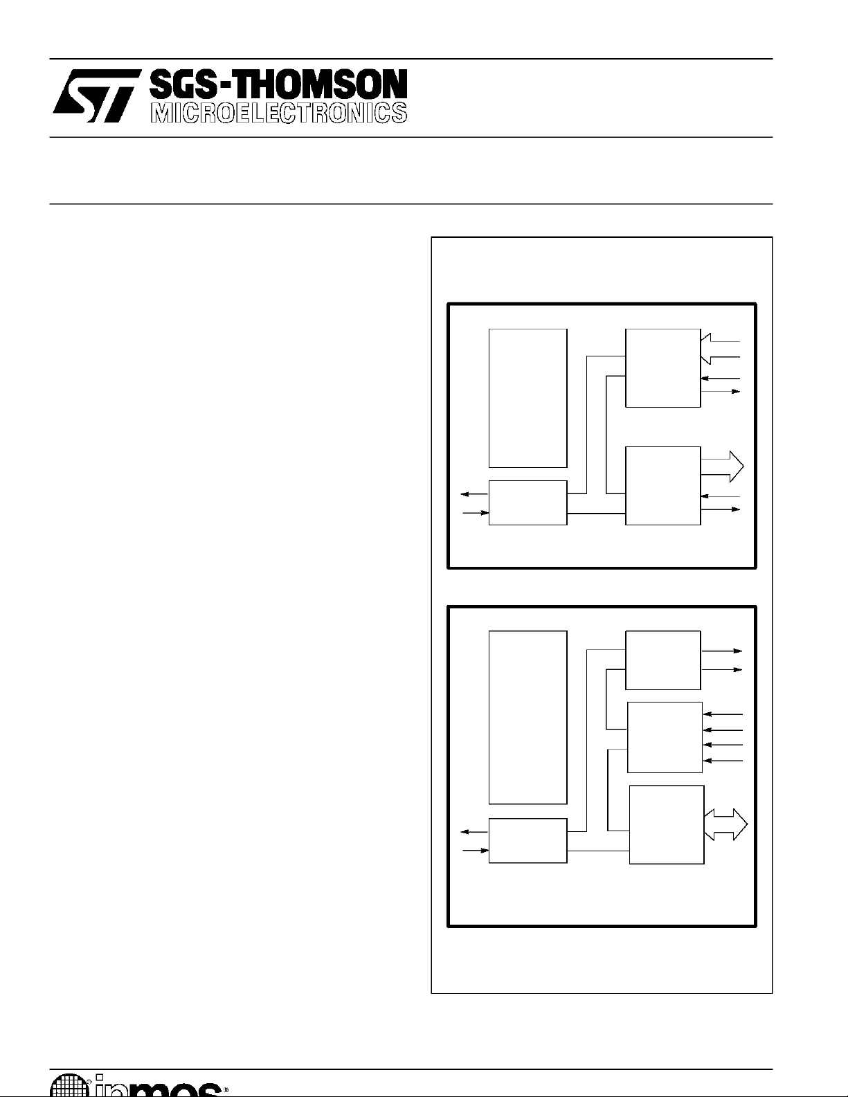
The link adaptor can be operated in one oftwo modes.In Mode 1the IMSC011converts between alink
and two independent fully handshaken byte-wide interfaces, oneinput and one output.It can be used by
a peripheral device to communicate with a transputer,a peripheral processor or another link adaptor, or
it can provide programmable input and output pins for a transputer. Two IMS C011 devices in this mode
can be connected back to back via the parallel ports and used as a frequency changer betweendifferent
speed links.
InMode 2 theIMS C011providesan interfacebetweenanINMOSseriallinkandamicroprocessorsystem
bus. Status and data registers for both input and output ports can be accessed across the byte-wide
bi-directional interface. Twointerrupt outputs are provided, one to indicate input data available and one
for output buffer empty.
VDD
GND
CapMinus
ClockIn
Reset
SeparateIQ
LinkOut
LinkIn
VDD
GND
CapMinus
ClockIn
Reset
SeparateIQ
LinkSpeed
LinkOut
LinkIn
Input
System
Services
Link
Figure 1.1 IMS C011 Mode 1 block diagram
System
Services
Link
Interface
Output
Interface
Interrupt
Control
Register
Select
Data and
Status
Registers
8
8
8
I0–7
IAck
IValid
Q0–7
Qack
QValid
InputInt
OutputInt
RS0
RS1
RnotW
notCS
D0–7
Figure 1.2 IMS C011 Mode 2 block diagram
3
/30
Page 4

2 Pin designations
Signal names are prefixed bynot if theyare active low,otherwise they are activehigh.
Pinout details for various packages are given on page 24.
Pin In/Out Function
VDD, GND Power supply and return
CapMinus External capacitor for internal clock power supply
ClockIn in Input clock
Reset in System reset
SeparateIQ in Select mode and Mode 1 link speed
LinkIn in Serial data input channel
LinkOut out Serial data output channel
Table 2.1 Services and link
Pin In/Out Function
I0-7 in Parallel input bus
IValid in Data on I0-7 is valid
IAck out Acknowledge I0-7 data received by other link
Q0-7 out Parallel output bus
QValid out Data onQ0-7 is valid
QAck in Acknowledge from device: data Q0-7 was read
IMS C011
Table 2.2 Mode 1 parallel interface
Pin In/Out Function
D0-7 in/out Bi-directional data bus
notCS in Chip select
RS0-1 in Register select
RnotW in Read/write control signal
InputInt out Interrupt on link receive buffer full
OutputInt out Interrupt on link transmit buffer empty
LinkSpeed in Select link speed as 10or 20 Mbits/sec
HoldToGND Must be connectedto GND
DoNotWire Must not be wired
Table 2.3 Mode 2 parallel interface
4
/30
Page 5
3 System services
3 System services
System services include all the necessary logic to start up and maintain the IMS C011.
3.1 Power
Power is supplied to the devicevia the VDD and GND pins. The supply mustbe decoupled close to the
chip by at least one 100 nF low inductance (e.g. ceramic) capacitor between VDD and GND. Four layer
boards are recommended; if two layer boards are used, extra care should be taken in decoupling.
AC noise between VDD and GND must be kept below 200 mV peak to peak at all frequencies above
100 KHz. AC noise between VDD and the ground reference of load capacitances must be kept below
200 mV peakto peak atall frequencies above 30 MHz. Input voltagesmust not exceed specification with
respect to VDD and GND, even during power-up and power-downramping, otherwise
CMOS devices can be permanently damaged by excessive periods of latchup.
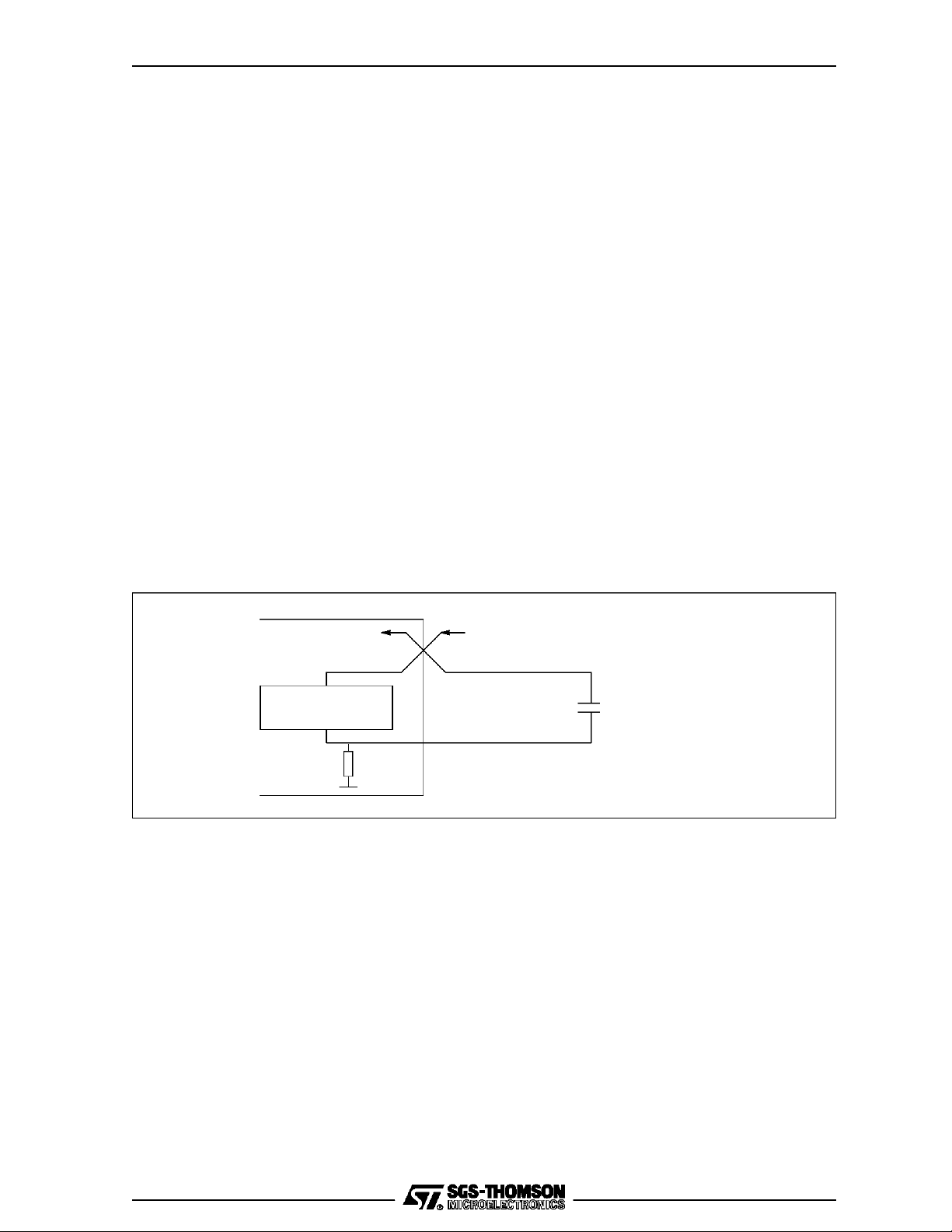
3.2 CapMinus
The internally derivedpower supply for internal clocks requires an external low leakage, low inductance
1F capacitor to be connected between VDD and CapMinus. A ceramic capacitor is preferred, with an
impedance less than 3 Ohms between 100 KHzand 10 MHz. If a polarised capacitor is used the negative
terminal should be connectedto CapMinus. TotalPCB track lengthshould be less than 50 mm. The positiveconnection ofthe capacitor mustbeconnecteddirectlytoVDD.Connectionsmust not otherwise touch
power supplies or other noisesources.
latchup
can occur.
VDD
P.C.B track
Decoupling
capacitor 1 F
Phase–locked
loops
GND
Figure 3.1 Recommended PLL decoupling
pin
VDD
CapMinus P.C.B track
3.3 ClockIn
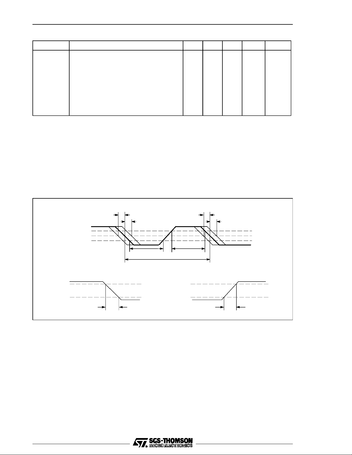
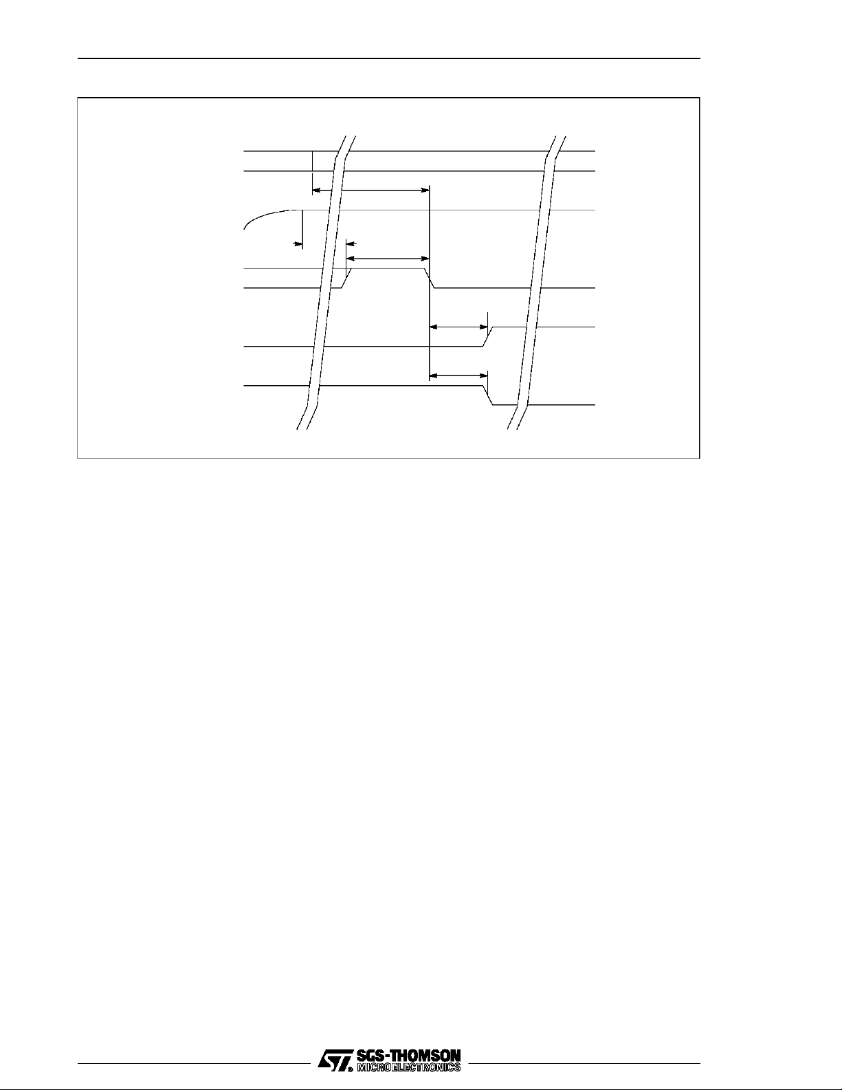
Transputerfamily components usea standardclock frequency,supplied bythe user on theClockIn input.
The nominal frequency of this clock for all transputer family components is 5 MHz, regardless of device
type, transputer word length or processor cycle time. High frequency internal clocks are derived from
ClockIn, simplifying system design and avoiding problems of distributing high speed clocks externally.
Anumberoftransputerfamilydevicesmay be connectedto acommon clock,ormay have individualclocks
providing each one meets the specified stability criteria. In a multi-clock system the relative phasing of
ClockIn clocks isnot important, due to theasynchronous natureof the links.Mark/space ratio is unimportant provided the specified limits of ClockIn pulse widths are met.
Oscillator stability is important. ClockIn must be derived from a crystal oscillator; RC oscillators are not
sufficiently stable. ClockIn must not be distributedthrough a longchain of buffers.Clock edges mustbe
monotonic and remain within the specified voltage and time limits.
/30
5
Page 6
IMS C011
Symbol Parameter Min Nom Max Units Notes
TDCLDCH ClockIn pulse width low 40 ns 1
TDCHDCL ClockIn pulse width high 40 ns 1
TDCLDCL ClockIn period 200 ns 1,2,4
TDCerror ClockIn timing error 0.5 ns 1,3
TDC1DC2 Difference in ClockIn for 2linked devices 400 ppm 1,4
TDCr ClockIn rise time 10 ns 1,5
TDCf ClockIn fall time 8 ns 1,5
Notes
1 Guaranteed, but not tested.
2 Measured between corresponding points on consecutive falling edges.
3 Variationof individual falling edgesfrom their nominal times.
4 This value allows the use of 200ppm crystal oscillatorsfor two devices connected together by
a link.
5 Clock transitions must be monotonic within the range VIH to VIL (table 7.3).
Table 3.1 Input clock
TDCerror
TDCerror
2.0V
1.5V
0.8V
TDCerror
TDCerror
TDCLDCH TDCHDCL
TDCLDCL
90%
10%
TDCf
90%
10%
TDCr
Figure 3.2 ClockIn timing
3.4 SeparateIQ
The IMS C011 link adaptor has two differentmodes of operation. Mode 1 is basically a link to peripheral
adaptor,whilst Mode 2 interfaces between a link and a microprocessor bus system.
Mode 1 can be selected for one of two link speeds by connectingSeparateIQ to VDD (10 Mbits/sec) or
to ClockIn (20 Mbits/sec).
Mode 2 is selected by connecting SeparateIQ to GND; in this mode 10 Mbits/sec or 20 Mbits/sec is selected byLinkSpeed. Link speeds arespecified for a ClockIn frequency of 5 MHz.
In order toselect thelink speed, SeparateIQ may be changeddynamically providing thelink is ina quiescentstateandno inputor outputisrequired.Resetmust beapplied subsequenttotheselectiontoinitialise
/30
6
Page 7
3 System services
the device. If ClockIn is gated to achieve this, its skew must be limited to the value TDCHSIQH shown
in table3.3. The mode of operation (Mode 1, Mode 2) must not be changed dynamically.
SeparateIQ Mode Link Speed Mbits/sec
VDD 110
ClockIn 120
GND 210or20
Table 3.2 SeparateIQ mode selection
Symbol Parameter Min Nom Max Units Notes
TDCHSIQH Skew fromClockIn to ClockIn 20 ns 1
Notes
1 Skew between ClockIn arriving on the ClockIn pin and on the SeparateIQ pin.
Table 3.3 SeparateIQ
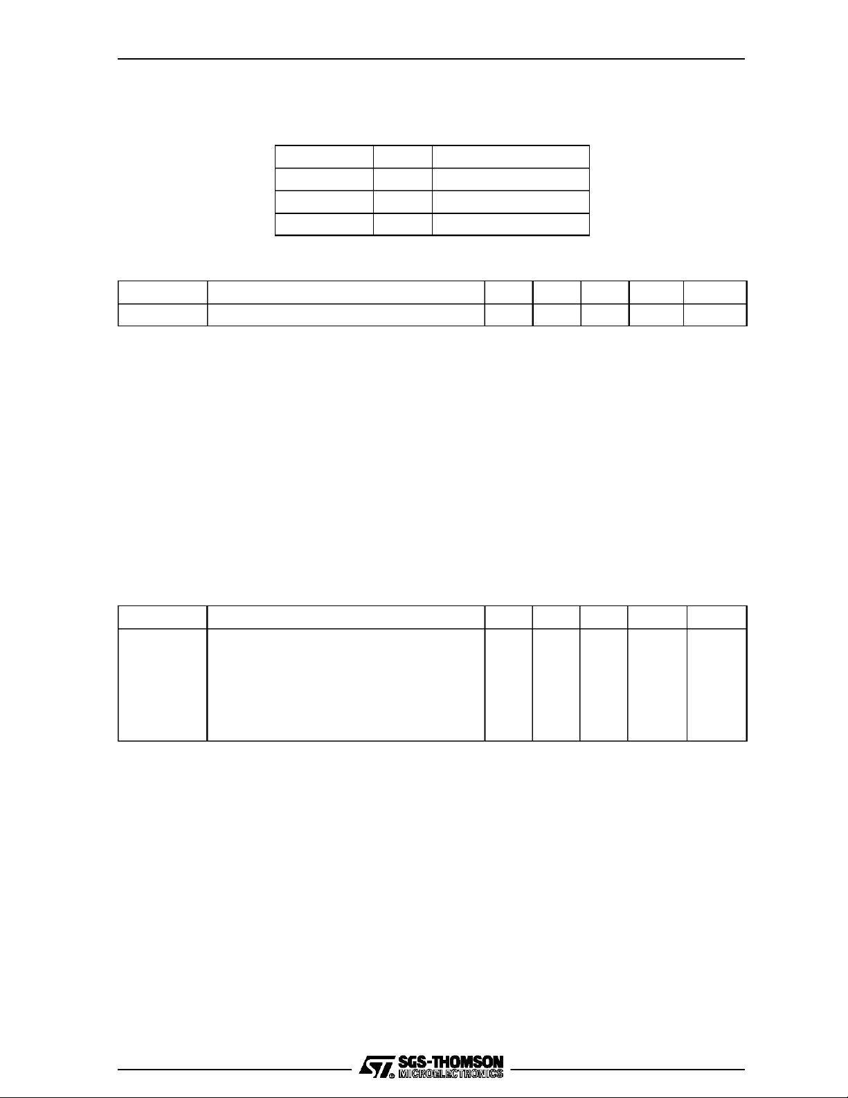
3.5 Reset
The Reset pin can go high withVDD, but must at no time exceed the maximumspecified voltageforVIH.
After VDD is valid ClockIn should be running for a minimum period TDCVRL before theendof Reset. All
inputs, with the exceptionof ClockIn and SeparateIQ (plus LinkSpeed in mode 2), must be heldin their
inactive state during reset.
Reset initialises theIMS C011to the following state: LinkOut is held low; the control outputs (IAck and
QValidin Mode 1, InputInt and OutputInt in Mode 2)are held low; interrupts (Mode2) are disabled; the
states of Q0-7 in Mode 1 are unspecified; D0-7 in Mode 2 are high impedance.
Symbol Parameter Min Nom Max Units Notes
TPVRH Power valid before Reset 10 ms
TRHRL Reset pulse width high 8 ClockIn 1
TDCVRL ClockIn running before Reset end 10 ms 2
TRLIvH Reset low before IValid high (mode 1) 0 ns
TRLCSL Reset low before chip select low (mode 2) 0 ns
Notes
1 Full periods of ClockIn TDCLDCL required.
2 At power-on reset.
Table 3.4 Reset
7
/30
Page 8
ClockIn
VDD
IMS C011
TDCVRL
Reset
IValid
notCS
TPVRH
TRHRL
TRLIvH
TRLCSL
Figure 3.3 Reset timing
8
/30
Page 9
4 Links
4 Links
INMOS bi-directional serial links provide synchronized communication between transputer productsand
with the outside world. Eachlink comprises aninput channel and output channel. A link between two devices is implemented byconnecting a link interface on onedevice to a link interfaceon the other device.
Everybyteof datasent onalinkis acknowledgedontheinput ofthesamelink,thus eachsignal line carries
both data and control information.
The quiescent state of a link output is low. Each data byte is transmitted as a high start bit followed by a
one bitfollowed by eight data bits followed bya low stopbit. The leastsignificant bit of data is transmitted
first. After transmitting a data byte the sender waits for the acknowledge,which consists of a high startbit
followed by a zero bit. The acknowledge signifies both that a process was able to receive the acknowledged data byte and that the receiving link is able to receive another byte.
Links are not synchronised with ClockIn and are insensitive to its phase. Thuslinks from independently
clockedsystemsmaycommunicate,providingonlythattheclocksarenominally identicaland withinspecification.
Links are TTL compatible andintended to be usedin electrically quietenvironments, between devices on
a singleprinted circuit board or between two boardsvia a backplane. Direct connectionmay be made between devices separated by a distance of less than 300 millimetres. For longer distances a matched
100 ohm transmissionline should be used with series matchingresistors RM. When this is donethe line
delay should be less than 0.4 bit time to ensure that the reflection returnsbefore the next databit is sent.
Buffers may be used for very long transmissions. If so, their overall propagation delay should be stable
within the skew tolerance of the link, although the absolute value of the delay is immaterial.
The IMS C011 link supports the standardINMOS communicationspeed of10 Mbits/sec. In addition it can
be used at 20Mbits/sec.Link speed canbe selectedin one of two ways.In Mode 1it is altered bySepara-
teIQ (page 6). In Mode 2 it is selected by LinkSpeed; when the LinkSpeed pin is low,the link operates
at the standard 10 Mbits/sec;when high it operates at 20 Mbits/sec.
HH L LH
01234567
Data
Figure 4.1 IMS C011link data and acknowledgepackets
Ack
9
/30
Page 10

IMS C011
Symbol Parameter Min Nom Max Units Notes
TJQr LinkOut rise time 20 ns 1
TJQf LinkOut fall time 10 ns 1
TJDr LinkIn rise time 20 ns 1
TJDf LinkIn fall time 20 ns 1
TJQJD Buffered edge delay 0 ns
TJBskew Variation in TJQJD 20 Mbits/s 3 ns 2
10 Mbits/s 10 ns 2
CLIZ LinkIn capacitance @ f=1MHz 7 pF 1
CLL LinkOut load capacitance 50 pF
RM Series resistor for 100W transmission line 56 ohms
Notes
1 Guaranteed, but not tested.
2 This is the variation in the total delay through buffers, transmission lines, differentialreceivers
etc., causedby such things as short term variation in supply voltages and differences in delays
for rising and fallingedges.
LinkOut
LinkIn
LinkOut
90%
10%
TJQr
90%
10%
Figure 4.2 IMS C011link timing
1.5 V
Latest TJQJD
Earliest TJQJD
Table 4.1 Link
TJDr
TJQf
TJDf
10
LinkIn 1.5 V
TJBskew
Figure 4.3 IMS C011buffered link timing
/30
Page 11

4 Links
Transputerfamily device A
LinkOut
LinkIn
Transputerfamily device A
LinkOut
LinkIn
Figure 4.5 Links connected by transmission line
Figure 4.4 Links directly connected
RM
Zo=100 ohms
Zo=100 ohms
RM
LinkIn
LinkOut
Transputer family device B
LinkIn
LinkOut
Transputer family device B
Transputerfamily device A
LinkOut
LinkIn
LinkIn
buffers
LinkOut
Transputer family device B
Figure 4.6 Links connected by buffers
11
/30
Page 12

IMS C011
5 Mode 1 parallel interface
In Mode 1 the IMS C011link adaptor is configured asa parallelperipheral interfacewith handshake lines.
Communication with a transputer family device is via theserial link. The parallel interface comprises an
input port and an output port, both with handshake.
5.1 Input port
The eight bit parallel inputport I0-7 can be readby a transputer family devicevia the seriallink.IValidand
IAck provide a simple two-wire handshake for this port. When data is valid on I0-7, IValid is taken high
by the peripheral deviceto commence thehandshake. The link adaptor transmits data presented on I0-7
outthroughtheseriallink.Afterthedatabytetransmissionhasbeen completedandanacknowledgepacket is received on the input link,the IMSC011sets IAck high. Tocomplete the handshake, the peripheral
device must return IValid low. The link adaptor will then set IAck low. New data should not be put onto
I0-7 until IAck is returned low.
Symbol Parameter Min Nom Max Units Notes
TIdVIvH Data setup 5 ns
TIvHLdV IValid high to link data output 0.8 2.5 bits 1,2
TLaVIaH Link acknowledge start to IAck high 3.5 bits 1,3
TIaHIdX Data hold after IAck high 0 ns
TIaHIvL IValid hold after IAck high 0 ns
TIvLIaL IAck hold after IValid low 0.8 3 bits 1
TIaLIvH Delay before next IValid high 0 ns
Notes
1 Unit of measurementis one link data bit time;at 10 Mbits/s data link speed, one bit time is nomi-
nally 100 ns.
2 Maximum timeassumes there isno acknowledge packetalready on thelink. Maximum time with
acknowledge on the link is extended by 2 bits.
3 Both data transmission and the returned acknowledge must be completed before IAck can go
high.
Table 5.1 Mode 1 parallel data input
I0–7
IValid
IAck
LinkOut
TIdVIvH
TIaHIvL TIaLIvH
TIvHLdV
Data
TLaVIaH
TIaHIdX
TIvLIaL
12
/30
LinkIn
Ack
Figure 5.1 IMS C011Mode 1 parallel data input to link adaptor
Page 13

5 Mode 1 parallel interface
5.2 Output port
The eight bit parallel output port Q0-7 can be controlled by a transputer family device via the serial link.
QValid and QAck provide a simple two-wire handshakefor this port.
A data packet received on the inputlink is presented on Q0-7; the linkadaptor then takes QValid high to
initiatethehandshake.After reading data fromQ0-7,theperipheral devicesetsQAck high. The IMSC011
will then send an acknowledge packet out of the serial link to indicate a completed transaction and set
QValid low to complete the handshake.
Symbol Parameter Min Nom Max Units Notes
TLdVQvH Start of link data to QValid 11.5 bits 1
TQdVQvH Data setup 12 ns 2
TQvHQaH QAck setup time fromQValid high 0 ns
TQaHQvL QAck high to QValid low 1.8 bits 1
TQaHLaV QAck high to Ack on link 0.8 2.5 bits 1,3
TQvLQaL QAck hold after QValid low 0 ns
TQvLQdX Data hold 11 bits 1,4
Notes
1 Unit of measurementis one link data bittime; at 10 Mbits/s data linkspeed, onebit timeisnomi-
nally 100 ns.
2 Where an existing data output bit is re-written with the same level there will be no glitch in the
output level.
3 Maximum time assumes thereis no data packet already onthe link.Maximum time with data on
the link is extended by 11 bits.
4 Data output remains valid until overwritten by new data.
Table 5.2 Mode 1 parallel data output
LinkIn
Q0–7
QValid
TLdVQvH
TQvHQaH
TQdVQvH
TQaHQvL
DataData
TQvLQdX
TQvLQaL
QAck
LinkOut
TQaHLaV
Ack
Figure 5.2 IMS C011Mode 1 parallel data output from link adaptor
13
/30
Page 14

IMS C011
6 Mode 2 parallel interface
The IMS C011provides aninterface between a link and a microprocessor stylebus.Operation of thelink
adaptor is controlled through the parallelinterface bus lines D0-7 by reading and writingvarious registers
in the link adaptor. Registers are selectedby RS0-1 and RnotW, and the chip enabled with notCS.
For convenience of description, the device connectedto the parallel side of thelink adaptor is presumed
to be a microprocessor, although this will not always be the case.
6.1 D0–7
Data is communicated between a microprocessor bus andthe link adaptor via thebidirectional bus lines
D0-7. The busis high impedance unless thelink adaptor chip is selected and the RnotW line is high. The
bus is used by the microprocessor to access status and data registers.
6.2 notCS
The link adaptor chip is selected when notCS is low.Register selectorsRS0-1 andRnotW must be valid
before notCS goes low; D0-7 must also be valid ifwriting to the chip (RnotW low). Data is read by the link
adaptor on the rising edge of notCS.
6.3 RnotW
RnotW,inconjunctionwithnotCS, selectsthe linkadaptor registersfor reador write mode. When RnotW
is high, the contents of an addressed register appearon the data busD0-7; when RnotW is low the data
onD0-7is writtenintothe addressedregister.The state ofRnotWislatched intothelinkadaptor by notCS
going low; it may be changed before notCS returns high, within the timing restrictions given.
6.4 RS0–1
One offour registers is selected by RS0-1. A register is addressed by setting up RS0-1 and then taking
notCSlow; the state of RnotW whennotCS goes low determineswhether the registerwill be read or writ-
ten. The state of RS0-1 is latched into the link adaptor by notCS going low; it may be changed before
notCS returns high, within the timing restrictions given. The register set comprises a read-only data input
register,a write-only data output register and a read/write status register for each.
RS1 RS0 RnotW Register
0 0 1 Read data
0 0 0 Invalid
0 1 1 Invalid
0 1 0 Write data
1 0 1 Read input status
1 0 0 Write input status
1 1 1 Read output status
1 1 0 Write output status
Table 6.1 IMS C011Mode 2 register selection
6.4.1 Input Data Register
This register holds thelast data packet received from theserial link. It never containsacknowledge packets. It contains valid data only whilst the
assumed to contain valid data after it has been read; a double read may ormay not return valid data on
the second read. If
to this register will have no effect.
/30
14
datapresent
isvalid ona subsequentread it indicates new data is in the buffer.Writing
data present
flag is set in the input status register. It cannot be
Page 15

6 Mode 2 parallel interface
Symbol Parameter Min Nom Max Units Notes
TRSVCSL Register selectsetup 5 ns
TCSLRSX Register selecthold 8 ns
TRWVCSL Read/write strobe setup 5 ns
TCSLRWX Read/write strobe hold 8 ns
TCSLCSH Chip select active 60 ns
TCSHCSL Delay before re-assertion of chip select 50 ns
Table 6.2 IMS C011Mode 2 parallel interface control
Symbol Parameter Min Nom Max Units Notes
TLdVIIH Start of link data to InputInt high 14 bits 1
TCSLIIL Chip select to InputInt low 35 ns
TCSLDrX Chip select to bus active 5 ns
TCSLDrV Chip select to data valid 50 ns
TCSHDrZ Chip select high to bus tristate 38 ns
TCSHDrX Data hold after chip select high 5 ns
TCSHLaV Chip de-select to start of Ack 0.8 2.5 bits 1,2
Notes
1 Unit of measurementis one link data bittime; at 10 Mbits/s data linkspeed, onebit timeisnomi-
nally 100 ns.
2 Maximum time assumes thereis no data packet already onthe link.Maximum time with data on
the link is extended by 11 bits.
Table 6.3 IMS C011Mode 2 parallel interface read
LinkIn
TLdVIIH
InputInt
TCSLIIL
RS0–1
TRSVCSL TCSLRSX
RnotW
TRWVCSL TCSLRSX
TCSLCSH TCSHCSL
notCS
DataData
D0–7
LinkOut
TCSLDrV
TCSLDrX
Figure 6.1 IMS C011Mode 2 read parallel data from link adaptor
TCSHDrZ
TCSHDrX
TCSHLaV
Ack
15
/30
Page 16

IMS C011
Symbol Parameter Min Nom Max Units Notes
TCSHDwV Data setup 10 ns
TCSHDwX Data hold 10 ns
TCSLOIL Chip select to OutputInt low 35 ns
TCSHLdV Chip select high to start of link data 0.8 2.5 bits 1,2
TLaVOIH Start of link Ack to OutputInt high 3.3 bits 1,3
TLdVOIH Start of link data to OutputInt high 13 bits 1,3
Notes
1 Unit of measurementis one link data bit time;at 10 Mbits/s data link speed, one bit time is nomi-
nally 100 ns.
2 Maximum timeassumes there isno acknowledge packetalready on thelink. Maximum time with
acknowledge on the link is extended by 2 bits.
3 Both datatransmissionand thereturned acknowledgemustbe completed before OutputInt can
go high.
Table 6.4 IMS C011Mode 2 parallelinterface write
RS0–1
RnotW
notCS
D0–7
OutputInt
LinkOut
LinkIn
TRSVCSL TCSLRSX
TRWVCSL
TCSLOIL
Figure 6.2 IMS C011 Mode 2 write parallel data to link adaptor
TCSLRWX
TCSLCSH
TCSHDwV
TCSHLdV
TCSHCSL
TCSHDwX
TLdVOIH
Data
TLaVOIH
Ack
16
/30
Page 17

6 Mode 2 parallel interface
6.4.2 Input Status Register
Thisregister contains the
ent
flag is set to indicate that data in the data input buffer is valid. It is reset lowonly when the datainput
buffer is read, or by Reset. When writing to this register, the
The
interruptenable
tively.Whenthe
tion 6.5). Resetting
register willset InputInt high again. The
When writing to this register, bits2-7 must be written as zero; this ensures that they will be zero when the
register is read.Failure to writezeroes to these bits may result in undefined data being returned bythese
bits during a status register read.
interrupt enable
765 43210
data present
bitcan be setandreset by writingtothestatus registerwiththis bit high or lowrespec-
interrupt enable
Figure 6.3 IMS C011Mode 2 input statusregister
flagand the
and
datapresent
will take InputInt low; setting it again before reading the data input
interrupt enable
interruptenable
flagsarebothhigh, the InputInt outputwillbe high(sec-
bit can be read to determine its status.
controlbitfor InputInt. The
data present
bit must be written as zero.
Interrupt
Enable
Data
Present
InputInt
&
datapres-
6.4.3 Output Data Register
Data written to this linkadaptor register is transmittedout of theserial link as a data packet. Datashould
onlybe writtentothis registerwhenthe
already being transmittedmay be corrupted. Readingthisregister willresult inundefined data beingread.
6.4.4 Output Status Register
This register contains the
ready
flagis setto indicate that the data outputbufferis emptyand alink acknowledge hasbeen received.
It is reset low only whendata is written to the data output buffer;it is set high by Reset. When writing to
this register, the
The
interruptenable
tively.When the
(section 6.6). Resetting
ister is emptywill setOutputInt high again. The
When writing to this register, bits2-7 must be written as zero; this ensures that they will be zero when the
register is read.Failure to writezeroes to these bits may result in undefined data being returned bythese
bits during a status register read.
output ready
interrupt enable
output ready
bit must be written as zero.
bitcan be setandreset by writingtothestatus registerwiththis bit high or lowrespec-
interrupt enable
output ready
flag and the
and
output ready
will takeOutputIntlow; settingit again whilstthe dataoutputreg-
bitin theoutputstatus register ishigh, otherwisedata
interrupt enable
flags are both high, the OutputInt output will be high
interrupt enable
control bit for OutputInt. The
bit can be read to determine itsstatus.
output
6.5 InputInt
The InputInt output is set high to indicate that a data packet has been received from the serial link. It is
inhibited from going high when the
InputInt is reset low when data is readfrom theinput data register (section 6.4.1)and by Reset (page 7).
interrupt enable
bit in the input status register is low (section 6.4.2).
/30
17
Page 18

IMS C011
765 43210
Interrupt
Enable
Figure 6.4 IMS C011Mode 2 output status register
Output
Ready
OutputInt
&
6.6 OutputInt
The OutputInt output is set high to indicate that the link is free to receive data from the microprocessor
for transmission as a data packet out of the serial link. It is inhibited from going high when the
enable
to thedata output register; it is set low by Reset (page 7).
bit in the output status register is low (section 6.4.4). OutputInt is reset low when data is written
interrupt
6.7 Data read
Adatapacket receivedontheinput linksetsthe
enable
respond to theinterrupt (if the
until the
Whendatais available from thelink, themicroprocessorreadsthedata packetfrom thedatainputregister.
This will resetthe
the serial link output.InputInt isautomatically reset by reading the data input register; it is not necessary
to reador write the input status register.
bitinthestatusregister isset, theInputInt outputpinwillbeset high.The microprocessorwilleither
interrupt enable
data present
bit is high.
data present
flag and cause the link adaptor to transmit anacknowledge packet out of
data present
bit is set) or willperiodically read the input status register
flagin the input statusregister.If the
interrupt
6.8 Data write
When the data output bufferis empty anda linkacknowledge has been received the
the outputstatus registeris set high. If the
output pin will also be set high.The microprocessor will eitherrespond to the interrupt (if the
able
bit is set) or will periodically read the output status register until the
When the
result in the link adaptor resetting the
out of the serial link. The
completedand an acknowledgepacketis received by theinputlink.This willsetthe
if the
output ready
interrupt enable
flag is high, the microprocessor can writedata to the data output buffer. This will
outputready
bit is set, OutputInt will also be set high.
interrupt enable
bit in the statusregister isset, the OutputInt
output ready
output ready
status bit will remain low until the data byte transmissionhas been
flag and commencing transmission of the data packet
output ready
interrupt en-
bit is high.
outputready
flag in
flag high;
18
/30
Page 19

7 Electrical specifications
7 Electrical specifications
7.1 DC electrical characteristics
SYMBOL PARAMETER MIN MAX UNITS NOTES
VDD DC supply voltage 0 7.0 V 1,2,3
VI,VO Voltage on input and output pins –0.5 VDD+0.5 V 1,2,3
II Input current
tOSC Output short circuit time (one pin) 1 s 2
TS Storage temperature –65 150
TA Ambient temperature under bias –55 125
PDmax Maximum allowable dissipation 600 mW
Notes
1 All voltages are with respect to GND.
2 This isa stressrating only and functionaloperation of thedevice atthese or any other conditions
beyond those indicated in the operating sections of this specification is not implied. Stresses
greater than those listed may cause permanent damage to the device. Exposure to absolute
maximum rating conditions for extended periods may affect reliability.
3 Thisdevicecontainscircuitry toprotecttheinputsagainst damagecausedbyhighstaticvoltages
or electrical fields. However, it is advised that normal precautions be taken toavoid application
of any voltage higherthan the absolutemaximum rated voltages to thishigh impedance circuit.
Unused inputs should be tied to an appropriate logic level such as VDD or GND.
4 The input current applies to any input or output pin and applies when the voltage on the pin is
between GND and VDD.
Table 7.1 Absolute maximum ratings
25
mA 4
o
C2
o
C2
SYMBOL PARAMETER MIN MAX UNITS NOTES
VDD DC supply voltage 4.75 5.25 V 1
VI,VO Input or output voltage 0 VDD V 1,2
CL Load capacitance on any pin 60 pF
TA Operating temperature range 0 70
Notes
1 All voltages are with respect to GND.
2 Excursions beyond the supplies are permitted but not recommended; see DC characteristics.
3 Air flow rate 400 linear ft/min transverse air flow.
Table 7.2 Operating conditions
o
C3
19
/30
Page 20

IMS C011
SYMBOL PARAMETER MIN MAX UNITS NOTES
VIH High level input voltage 2.0§ VDD+0.5 V 1, 2
VIL Low level input voltage –0.5 0.8 V 1, 2
II Input current @ GND<VI<VDD 10 mA1,2,3
200 mA
VOH Output high voltage @ IOH=2mA VDD–1 V 1, 2
VOL Output low voltage @ IOL=4mA 0.4 V 1, 2
IOZ Tristateoutput current @ GND<V0<VDD
PD Power dissipation 120 mW 2, 5
CIN Input capacitance @ f=1MHz 7 pF 6
COZ Output capacitance @ f=1MHz 10 pF 6
§For RnotW, RS0-1, SeparateIQ over temperature range –40<TA<25oC (where applicable), substitute 2.2V.
Notes
1 All voltages are with respect toGND.
10 mA
1, 2, 4
1, 2
2 Parameters for IMS C011measured at 4.75V<VDD<5.25V and0oC<TA<70oC.
3 For inputs other than those in Note 4.
4 For pins 2, 3, 5, 6, 7, 9, 11, 13, 15, 16, 25.
5 Power dissipationvaries with output loading.
6 Guaranteed, but not tested.
Table 7.3 DC characteristics
7.2 Equivalent circuits
IOL
1.5V
D.U.T.
1MW
IOH
Note:This circuitrepresents thedevice sinkingIOLand sourcingIOHwitha50pFcapacitiveload.
Figure 7.1 Load circuit for AC measurements
/30
20
50pF
GND
Page 21

7 Electrical specifications
VDD–1
Inputs
0V
VDD–1
Inputs
0V
VDD
Outputs
0V
VDD
Outputs
0V
Figure 7.2 AC measurements timing waveforms
7.3 AC timing characteristics
VIH
VIL
tpHL
1.5V
tpLH
1.5V
SYMBOL PARAMETER MIN MAX UNITS NOTES
TDr Input rising edges 2 20 ns 1, 2, 3
TDf Input falling edges 2 20 ns 1, 2, 3
TQr Output rising edges 25 ns 1, 3
TQf Output falling edges 15 ns 1, 3
Notes
1 Non-link pins; see section on links.
2 All inputs except ClockIn; see section on ClockIn.
3 Guaranteed, but not tested.
Table 7.4 Input and output edges
21
/30
Page 22

IMS C011
90%
10%
90%
10%
1.5 V
TCSHDrHZ
TDf
TQf
90%
10%
TDr
90%
10%
TQr
Figure 7.3 IMS C011 input and output edge timing
1.5 V
TCSHDrLZ
Time
ns
30
20
10
90%
10%
Figure 7.4 IMS C011tristate timing relative tonotCS
30
Rise time
20
Time
Fall time
40 60 80 100
Load capacitance pF
Link
Figure 7.5 Typicalrise/fall times
ns
10
Rise time
Fall time
40 60 80 100
Load capacitance pF
Non Links
22
/30
Page 23

7 Electrical specifications
7.4 Power rating
Internal power dissipation (P
figure 7.6. P
is substantially independent of temperature.
INT
) of transputer and peripheral chips depends on VDD, as shown in
INT
200
150
Power
P
INT
(mW)
100
50
4.4 4.6 5.0 5.6
4.8 5.2 5.4
VDD (Volts)
Figure 7.6 IMS C011internal power dissipation vs VDD
Total power dissipation (PD) of the chip is
P
=
P
+
INT
P
IO
D
where PIOis the power dissipation inthe input and output pins; this isapplication dependent.
Internal working temperature TJof the chip is
T
=
T
+
A
q
JA*PD
J
where TAis the external ambient temperature inoC and qJAis the junction-to-ambientthermal resistance
inoC/W.
Information about device thermal management can be found in the following SGS-THOMSON catalogues, available from SGS-THOMSON sales officesand authorized distributors worldwide.
1
Thermal Management in SurfaceMount Technology
2
Reliability in Surface Mount Technology
, order code: BRRELSMT/1088
, order code: BRTHERMAN/0788
23
/30
Page 24

8 Package details
8.1 Package pinouts
IMS C011
24
Figure 8.1 IMS C011package pinouts
/30
Page 25

8 Package details
8.2 28-pin plastic DIL package dimensions
Figure 8.2 IMSC011 28-pin plastic dual-in-line package dimensions
25
/30
Page 26

8.3 28-pin SOJ package dimensions
IMS C011
26
Figure 8.3 IMSC011 28-pin SOJ package dimensions
/30
Page 27

8 Package details
8.4 28-pin LCCC package dimensions
Figure 8.4 IMSC011 28-lead chip carrier (LCC) package dimensions
27
/30
Page 28

IMS C011
8.5 Thermal specification
The IMS C011is testedto a maximum silicontemperature of100_C. Foroperationwithinthe given specifications, the case temperature should not exceed 85_C.
For temperatures above 85_C the operation of the device cannot be guaranteed and reliability may be
impaired.
For further information on reliability referto the SGS–THOMSONMicroelectronics Quality and Reliability
Program.
28
/30
Page 29

9 Ordering
9 Ordering
Thissection indicates thedesignation of packageselections fortheIMS C011.Speed ofClockInis 5 MHz
for all parts.
For availability contact your local SGS–THOMSON sales office or authorized distributor.
SGS–THOMSON designation Package
IMS C011-P20S 28 pin plastic dual-in-line
IMS C011-E20S 28 pin SOJ
IMS C011-W20S 28 pin LCCC non-solder dip
Table 9.1 IMS C011ordering details
An extended temperature version is available, see the
IMS C011E Datasheet
for details.
29
/30
Page 30

IMS C011
Information furnished is believed to be accurate and reliable. However, SGS-THOMSON Microelectronics assumes no
responsibility for the consequences of use of such information nor for any infringement of patents or other rights of third
parties which may result from its use. No license is granted by implicationor otherwise under any patent or patent rights of
SGS-THOMSON Microelectronics. Specifications mentioned in this publication are subject to change without notice. This
publication supersedesand replacesall information previouslysupplied.SGS-THOMSONMicroelectronicsproducts arenot
authorizedfor use as critical components in life support devicesorsystemswithout express writtenapproval ofSGS-THOMSON Microelectronics.
E 1995 SGS-THOMSON Microelectronics - All Rights Reserved
, , IMS,
Australia - Brazil - France - Germany - Hong Kong - Italy - Japan - Korea - Malaysia - Malta - Morocco -
The Netherlands - Singapore - Spain - Sweden - Switzerland - Taiwan - Thailand - United Kingdom - U.S.A.
/30
30
occam and DS-Link are trademarks of SGS-THOMSON Microelectronics Limited.
is a registered trademarkof the SGS-THOMSON Microelectronics Group.
SGS-THOMSON Microelectronics GROUP OF COMPANIES
 Loading...