

Datasheet IMP37-33JST, IMP37-33JCM, IMP37-30JST, IMP37-25JST, IMP37-30JCM Datasheet (IMP)
...Page 1
©
1999 IMP, Inc. 408-432-9100/www.impweb.com 1
Key Features
Applications
◆ High-efficiency linear power supplies
◆ Post regulator for switching supplies
◆ 5V to 3.3V linear regulators
◆ USB hubs
◆ Battery chargers
◆ Routers, ISDN/DSL modems
◆
Low Dropout Voltage
– 0.8V maximum at 100mA
– 0.95V maximum at 800mA
– 20% lower dropout voltage than “1117”
LDO regulators
◆
Guaranteed Low Dropout Voltage at Multiple
Current Levels
◆
1% Trimmed 2.5V, 3.0V and 3.3V Outputs
◆
Reduced Quiescent Current: 75µA Maximum
◆
Short Circuit and Thermal Protection
◆
Space Saving SOT-223 Surface Mount Package
◆
“1117” Pin Compatible
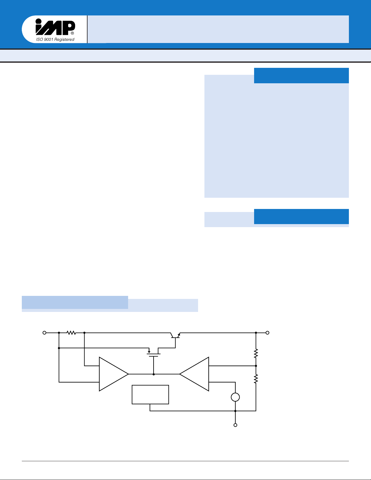
Block Diagram
IMP3
IMP377
POWER MANAGEMENT
Lo
Lo
w Dr
w Dr
opout P
opout P
ositiv
ositive e
VVolt
oltagag
e R
e R
egulat
egulatororss
– 800mA
– 800mA
– 2.5V
– 2.5V
, 3.0V and 3.3V Output
, 3.0V and 3.3V Output
The IMP37 series of Low Dropout (LDO) three-terminal voltage regulators feature guaranteed low dropout voltages at currents up to 0.8A. The
IMP37 regulator family dropout voltage is guaranteed to be 0.95V or
lower at 0.8A. At 100mA, the maximum dropout voltage is 0.8V.
Compared with “1117” type LDOs, the IMP37 has a 20% lower dropout
voltage.
Three fixed output voltages are offered: 2.5V, 3.0V and 3.3V. Output voltages are factory trimmed to within 1% of the nominal value.
In addition to low dropout voltages, the IMP37 family features greatly
reduced quiescent operating current. The 75µA maximum specification
represents an over 100 times improvement over competitive devices.
Devices are short circuit protected, and a thermal protection circuit shuts
the regulator off should the junction temperature exceed 165°C.
The IMP37 is available in low-profile plastic SOT-223 and TO-263
packages and are pin compatible with fixed “1117” devices.
R
Input
3
CS
Current
Limit
2
Out
(Tab)
IMP37
Error
+
–
Thermal
Protection
Amp
–
+
+
Ref
–
1
GND
37_01.eps
Page 2
2
408-432-9100/www.impweb.com
©
1999 IMP, Inc.
Pin Configuration
IMP3
IMP377
Pin Descriptions
Package Marking Code
Ordering Information
IMP37
37_05.eps
GND
INPUT
1
3
OUT
TAB IS V
OUT
2
SOT-223 TO-263
Front View Front View
rebmuNtraPegakcaP
eciveD
gnikraM
TSJ52-73PMI322-TOS5273
TSJ03-73PMI322-TOS0373
TSJ33-73PMI322-TOS3373
MCJ52-73PMI362-OTMCJ5273
MCJ03-73PMI362-OTMCJ0373
MCJ33-73PMI362-OTMCJ3373
spe.50elbaT_73
snoitpOtuptuOrebmuNgniredrOtraP
egatloV
mumixaM
tnerruCtnecseiuQ
taegatloVtuoporD
Am008
322-TOS
egakcaP
362-OT
egakcaP
V5.257µAV59.0TSJ52-73PMIMCJ52-73PMI
V0.357µAV59.0TSJ03-73PMIMCJ03-73PMI
V3.357µAV59.0TSJ33-73PMIMCJ33-73PMI
spe.60t_73
Note: Tape and reel shipping is available for the SOT-223 and TO-263 packages. Append the TAPE AND REEL designation “/T” to the ordering
part number for tape and reel devices. For example, the IMP37-25JST/T is a 2.5V SOT-223 packaged device shipped in reels.
rebmuNniPemaNnoitcnuF
1DNGniPdnuorG
2TUOegatloVtuptuO
3TUPNIegatloVtupnI
BATBATegatloVtuptuO
spe.30elbaT_73
INPUT
3
TAB IS V
OUT
IMP37
OUT2
GND
1
37_04.eps
Page 3

©
1999 IMP, Inc. 408-432-9100/www.impweb.com 3
IMP3
IMP377
Absolute Maximum Ratings
Electrical Characteristics
Input Voltage . . . . . . . . . . . . . . . . . . . . . . . . . 7V
Operating Junction Temperature . . . . . . . . . 0°C to 150°C
Storage Temperature Range . . . . . . . . . . . . . –65°C to +150°C
Lead Temperature (Soldering) . . . . . . . . . . . . . 300°C for 10 seconds
These are stress ratings only and functional operation is not implied.
Exposure to absolute maximum ratings for prolonged time periods may
affect device reliability. All voltages are with respect to ground.
Specifications apply over the junction operating temperature range of T
J
= 0°C to +125°C unless otherwise noted.
Notes: 1. See thermal regulation specification for changes in output voltage due to heating effects. Load regulation and line regulation
are measured with low duty cycle pulse testing to maintain a constant junction temperature.
2. Dropout voltage is specified over the full output current range. Dropout voltage is defined as the minimum input/output
differential measured at the specified output current.
3. Minimum load current is defined as the minimum output current required to maintain regulation.
retemaraPlobmySxiffuSsnoitidnoCniMpyTxaMstinU
egatloVtuptuOV
TUO
52–I
TUO
V,Am01=
NI
T,V58.4=
J
52=C°574.25.2525.2V
Am01≤I
TUO
≤I
XAM
V52.4,≤V
NI
≤V5.554.25.255.2
03–
I
TUO
V,Am01=
NI
T,V5=
J
52=C°79.200.330.3
Am01≤I
TUO
≤I
XAM
V57.4,≤V
NI
≤V5.549.200.360.3
33–I
TUO
V,Am01=
NI
T,V5=
J
52=C°762.303.3333.3
Am01≤I
TUO
≤I
XAM
V57.4,≤V
NI
≤V5.5532.303.3563.3
noitalugeReniL
)1etoN(
52–I
TUO
V52.4,Am01= (≤VNI)≤V5.52191
Vm
03–I
TUO
V5.4,Am01= ≤VNI≤V5.52191
33–I
TUO
V5.4,Am01= ≤VNI≤V5.52191
noitalugeReniL
)1etoN(
52–I
TUO
V52.4,Am01= (≤VNI)≤T,V5.5
A
52=C°8.23.4
Vm
03–I
TUO
V5.4,Am01= ≤VNI≤T,V5.5
A
52=C°8.23.4
33–I
TUO
V5.4,Am01= ≤VNI≤T,V5.5
A
52=C°8.23.4
noitalugeRdaoL
)1etoN(
52–V
NI
Am5,V52.4= ≤I
TUO
≤Am0085203Vm
03–V
NI
Am5,V57.4= ≤I
TUO
≤Am0085203
33–V
NI
Am5,V57.4= ≤I
TUO
≤Am0085203
egatloVtuoporD
)2etoN(
xx–
I
TUO
Am001=8.0V
I
TUO
Am008=59.0
timiLtnerruCI
)XAM(TUO
xx–T
J
52=C°0080590021Am
tnerruCdaoLmuminiMxx– 0.5Am
tnerruCtnecseiuQI
Q
xx–VNI≤V66357
µA
noitalugeRlamrehTT
A
52=C°esluPsm03,10.01.0W/%
noitcejeRelppiRf
ELPPIR
V,zH021=
NI
T,V5=
A
52=C°
V
ELPPIR
I,p-pV1=
DAOL
Am01=
1545Bd
ytilibatSerutarepmeT 5.0%
ytilibatSmreTgnoLT
A
521=C°srH0001,3.0%
esioNtuptuOSMRVfo%(
TUO
zH01,)≤f≤T,zHk01
J
52=C°300.0%
ecnatsiseRlamrehT )322-OT(BATtaesaC-ot-noitcnuJ51°W/C
)362-OT(BATtaesaC-ot-noitcnuJ01
spe.70t_73
Page 4

4
408-432-9100/www.impweb.com
©
1999 IMP, Inc.
IMP3
IMP377
Application Information
The IMP37 voltage regulator ICs offer self-protection features
which include short-circuit current protection and automatic thermal
shutdown (for junction temperature above 165°C).
Circuit Stability
Like all regulators, an output filter capacitor is required for circuit stability. Besides smoothing the output, the output capacitor
“completes” the regulator’s frequency compensation. The ESR of the
output capacitor should be less than 0.5Ω. Low ESR capacitors are
preferred.
Table 1 shows recommended minimum capacitance values for both
aluminum and tantalum capacitors. Larger values of output capacitance do not cause stability problems.
Table 1. Recommended Output Bypass Capacitors
An input bypass capacitor is recommended. A 10µF or larger tanta-
lum capacitor is suitable for most applications.
Figure 1. Fixed 3.3V Regulator
Thermal Management
The maximum operating junction temperature for the IMP37 devices
is 150°C. The junction temperature can be calculated when the
power dissipation and ambient temperature are known with this
equation: T
J
= TA+ (P
D
x Θ
JA
).
The thermal resistance from juntion-to-ambient (Θ
JA
) is the sum of
the three thermal resistances:
Θ
JA
= ΘJT+ ΘTS+ Θ
SA
Where Θ
JT
= Junction-to-Tab thermal resistance
Θ
TS
= Tab-to-Heat Sink thermal resistance
Θ
SA
= Heat Sink-to-Air thermal resistance
Table 2. Thermal Resistance of Packages
The IMP37 series devices have thermal limiting circuitry to protect
the device from over current. For continuous operation, the maximum junction temperature rating must not be exceeded.
epyTegakcaP
ecnatsiseRlamrehT
,baTotnoitcnuJ Θ
TJ
322-TOS 51 ° W/C
362-OT 01 ° W/C
IMP37
OUTV
IN
* **
IN 3.3V
37_02.eps
GND
* Min. 15µF Tantalum or 100µF Aluminum.
Capacitor May Be Increased Without Limit.
** 10µF Tantalum or 100µF Aluminum
++
5.0<RSE(roticapaCssapyBtuptuO Ω)
01 µ 001,mulatnaTF µ munimulAF
Page 5

IMP3
IMP377
©
1999 IMP, Inc. 408-432-9100/www.impweb.com 5
Package Dimensions
Plastic SOT-223 (4-Pin)
E
A
e1
A1
C
H
e
D
S
B1
B
Q2
Q1
Q
SOT-223 (4-Pin).eps
TO-263 (3-Pin)
D
L
E
e
B2
B
A
L2
C2
L1
C
0° - 8°
TO-263 (3-Pin).eps
sehcnI sretemilliM
niM xaM niM xaM
*)niP-4(322-TOScitsalP
A 760.0 060.0 07.1 05.1
1A 400.0 8000.0 01.0 20.0
B 421.0 611.0 51.3 59.2
1B 330.0 620.0 58.0 56.0
C 410.0 010.0 53.0 52.0
D 462.0 842.0 07.6 03.6
e MON5090.0 MON03.2
1e MON181.0 MON05.4
E 641.0 031.0 07.3 03.3
h 782.0 462.0 03.7 07.6
S 140.0 330.0 50.1 58.0
t 150.0 340.0 03.1 01.1
Q XAM°01 XAM°01
1Q °61 °01 °61 °01
2Q °61 °01 °61 °01
**)niP-3(362-OT
A 061.0 091.0
B 020.0 930.0
2B 540.0 550.0
C 810.0 920.0
2C 540.0 550.0
D 043.0 083.0
E 083.0 504.0
e CSB001.0
L 575.0 526.0
1L 090.0 011.0
2L ——— 550.0
AA162-OTgniwarDCEDEJ*
AA362-OTgniwarDCEDEJ**
♦
.leeRdnaepaTrofrebmuNtraPotT/ddA
spe.40elbaT_73
Page 6

IMP3
IMP377
IMP, Inc.
Corporate Headquarters
2830 N. First Street
San Jose, CA 95134-2071
Tel: 408-432-9100
Tel: 800-438-3722
Fax: 408-434-0335
Fax-on-Demand: 1-800-249-1614 (USA)
Fax-on-Demand: 1-303-575-6156 (International)
e-mail: info@impinc.com
http://www.impweb.com
The IMP logo is a registered trademark of IMP, Inc.
All other company and product names are trademarks of their respective owners.
© 1999 IMP, Inc.
Printed in USA
Publication #: 8002
Revision: C
Issue Date: 07/22/99
Type: Preliminary
 Loading...