

Page 1
SN65LVDS324
www.ti.com
SLLSED9 –NOVEMBER 2012
1080p60 IMAGE SENSOR RECEIVER
Check for Samples: SN65LVDS324
1
FEATURES
23
• Bridges the Interface Between Video Image
Sensors and Processors
• Receives Aptina HiSPi™, Panasonic LVDS, or
Sony LVDS Parallel; Outputs 1.8V CMOS with
10/12/14/16 Bits at 18.5MHz to 162MHz
• SubLVDS Inputs Support Up To 648Mbps
• Integrated 100Ω Differential Input Termination
• Test Image Generation Feature
• Compatible with TI OMAP™ and DaVinci™
Including DM385, DM8127, DM36x, and DMVA
DESCRIPTION
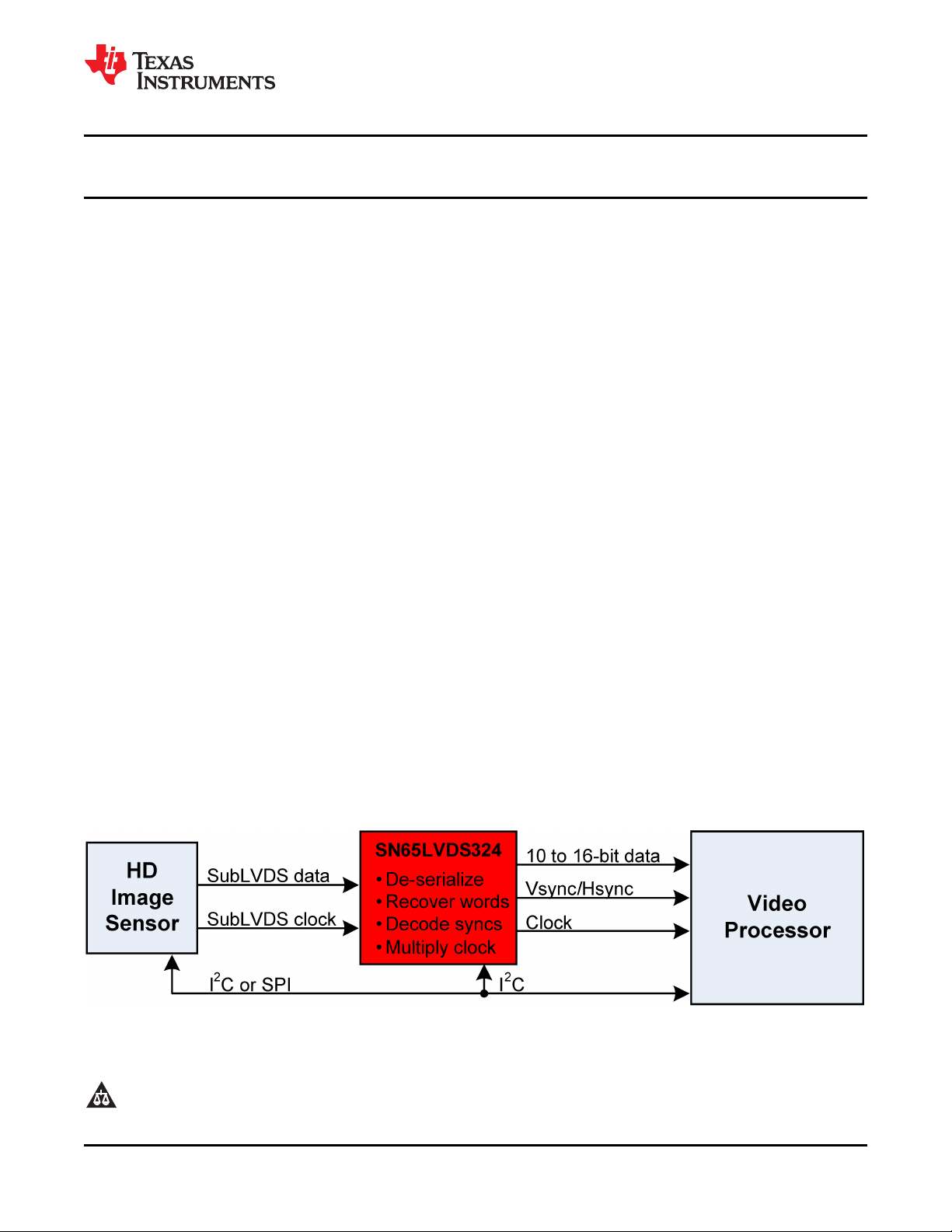
The SN65LVDS324 is a SubLVDS deserializer that recovers words, detects sync codes, multiplies the input DDR
clock by a ratio, and outputs parallel CMOS 1.8V data on the rising clock edge. It bridges the video stream
interface between HD image sensors made by leading manufacturers, to a format that common processors can
accept. The supported pixel frequency is 18.5MHz to 162MHz — suitable for resolutions from VGA to 1080p60.
Four high-level modes are supported: Aptina 1-Channel 4-Lane, Aptina 1-Channel 2-Lane, Panasonic 2-Channel
2-Port, and Sony LVDS Parallel. Each supports 10/12/14/16 bit sub-modes, according to Table 1. Each mode
also has a configurable allowable frequency range, as specified by Table 3 register PLL_CFG.
The SN65LVDS324 is configured through its I2C-programmable registers. This volatile memory must be written
after power up. Configuration options include the MSB/LSB output order, sync polarity convention, data slew
rate, and two output timing modes (long-setup or clock-centered), for wider compatibility with different processors
and software. The TESTMODE_VIDEO feature is designed to assist engineering development. The max
allowable frame size is 8191 x 8191.
• Low Power 1.8V CMOS Process
• Configurable Output Conventions
• Packaged in 4.5 x 7mm BGA
APPLICATIONS
• IP Network Cameras
• Machine Vision
• Video Conferencing
• Gesture Recognition
With integrated differential input termination, and a footprint of 4.5 x 7mm, the SN65LVDS324 provides a
differentiated solution with optimized form, function, and cost. It operates through an ambient temperature range
of –40°C to 85°C.
spacer
spacer
Figure 1. General System Diagram
1
Please be aware that an important notice concerning availability, standard warranty, and use in critical applications of
Texas Instruments semiconductor products and disclaimers thereto appears at the end of this data sheet.
2OMAP, DaVinci are trademarks of Texas Instruments.
3HiSPi is a trademark of Aptina.
PRODUCTION DATA information is current as of publication date.
Products conform to specifications per the terms of the Texas
Instruments standard warranty. Production processing does not
necessarily include testingof all parameters.
Copyright © 2012, Texas Instruments Incorporated
Page 2
C
V
CC
SN65LVDS324
R = 150 k
RST
Ω
RST
V
CC
C
SN65LVDS324
GPO
Controller
R = 150 k
RST
Ω
RST
Control Logic and
(Control and Status Registers)
SDA
SCL
D15
D0
VSYNC
HSYNC
CLKOUT
SD9P
SD9N
100Ω
4b
1-Channel 4-Lane
1-Channel 2-Lane
Word Recovery
and SYNC Decode
4b
2-Channel 2-Port
Word Recovery
and SYNC Decode
12b
LVDS Parallel
SYNC Decoder
100Ω
SD0P
SD0N
100Ω
SCLKP
SCLKN
Clock Generator
PLL
CLK * (1/3, 1/2, 2/3, 4/7, 2)
12b
Parallel Output Protocol Engine
16b
SOF/EOF
SOL/EOL
RST
VCC
GND
VCCA
GNDA
SD10P
SD10N
100Ω
SD11P
SD11N
100Ω
HS
VS
16b
SOF/EOF
SOL/EOL
16b
SOF/EOF
SOL/EOL
DDR LVDS Receiver
Parallel Interface
I2C
SN65LVDS324
SLLSED9 –NOVEMBER 2012
This integrated circuit can be damaged by ESD. Texas Instruments recommends that all integrated circuits be handled with
appropriate precautions. Failure to observe proper handling and installation procedures can cause damage.
ESD damage can range from subtle performance degradation to complete device failure. Precision integrated circuits may be more
susceptible to damage because very small parametric changes could cause the device not to meet its published specifications.
FUNCTIONAL DESCRIPTION
www.ti.com
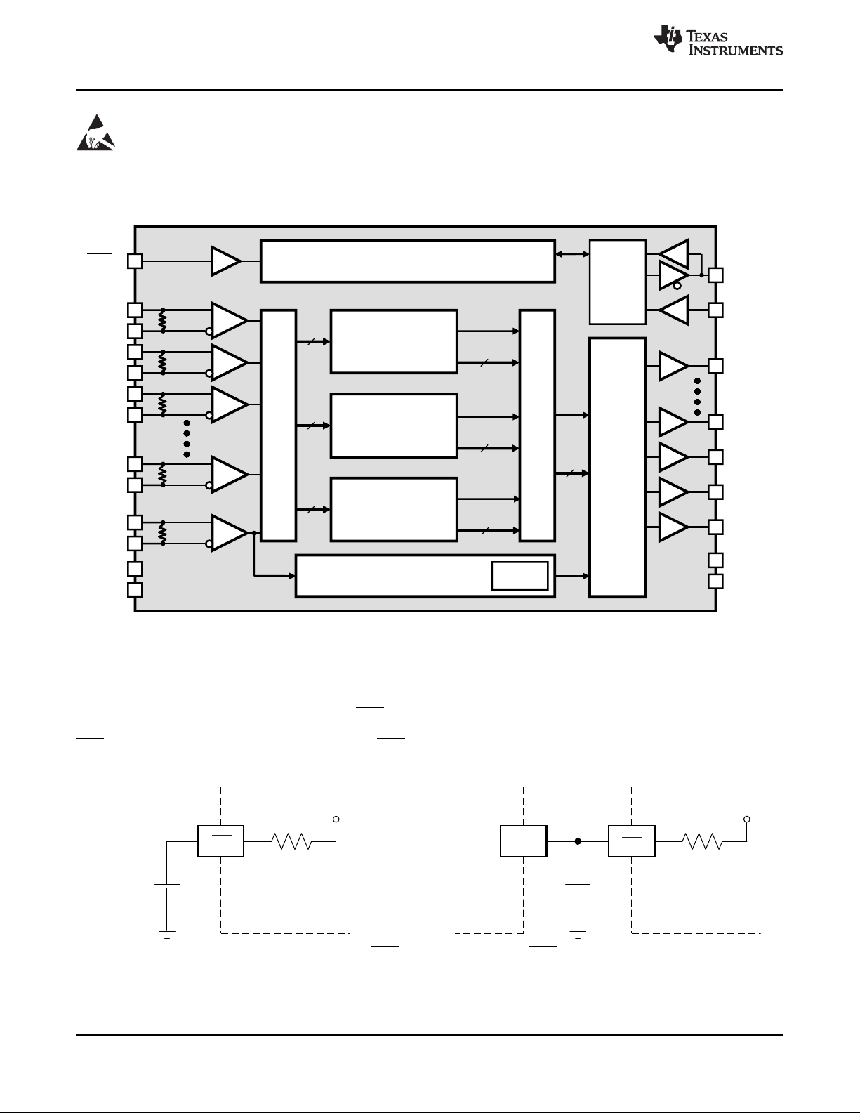
Figure 2. Functional Block Diagram
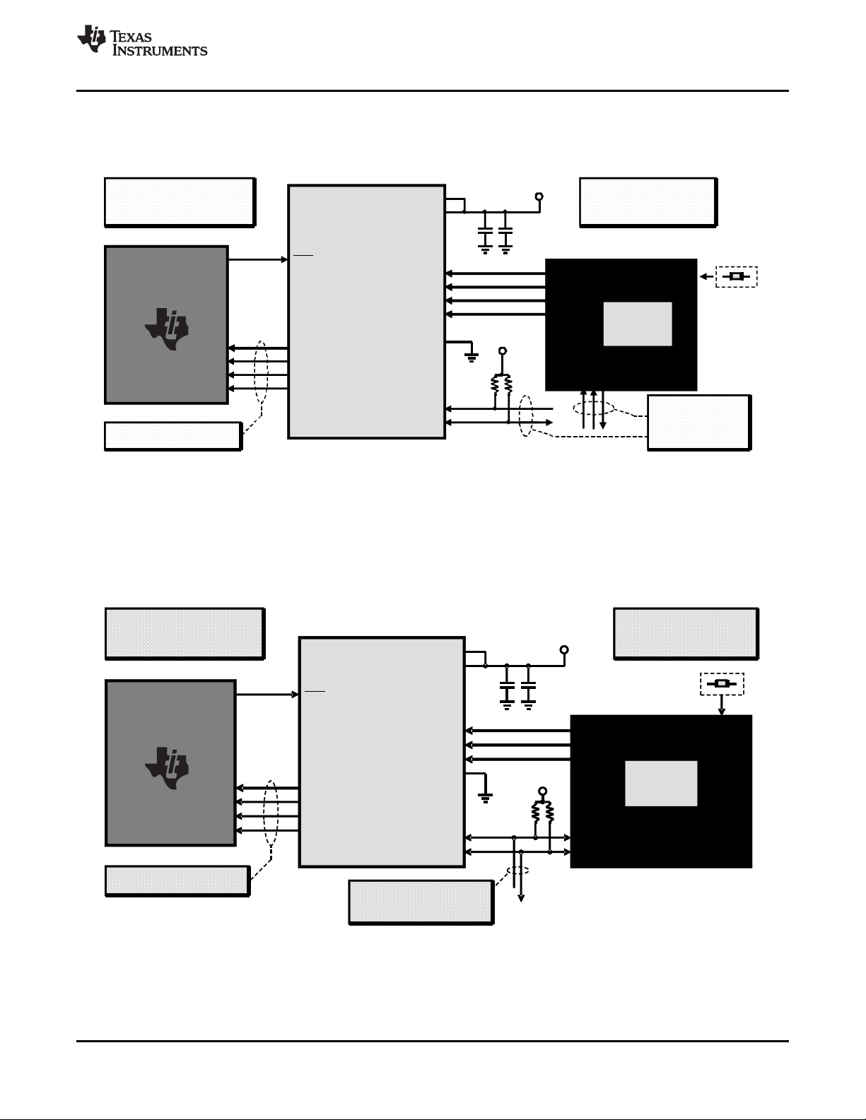
Reset Implementation
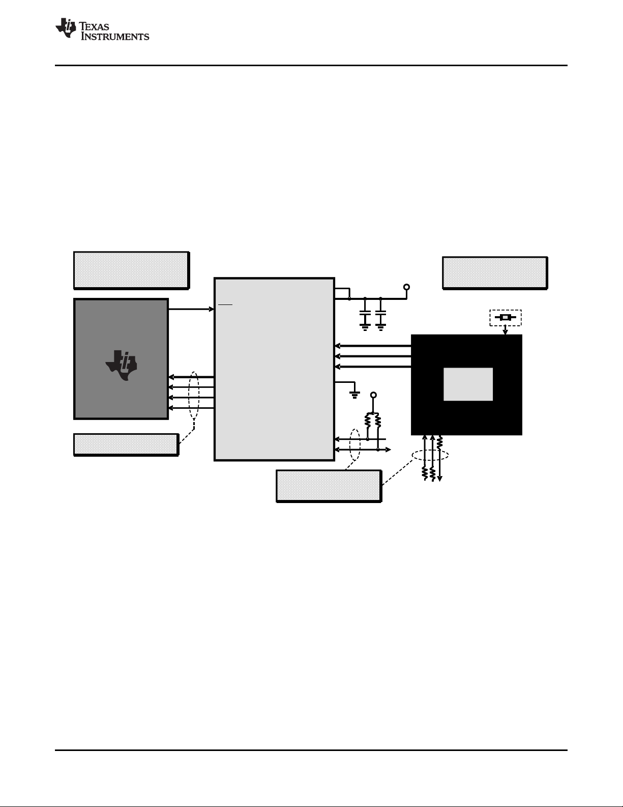
When RST is Low, the PLL is disabled, the SubLVDS inputs are disabled, and all outputs drive either VOHor V
with no toggling. It is critical to transition the RST input from a low to high level after the VCCsupply has reached
the minimum recommended operating voltage. This is achieved by an external capacitor connected between
RST and GND, and/or by a control signal to the RST input. Both implementations are shown:
Figure 3. External Capacitor Controlled RST Figure 4. RST Input from Active Controller
2 Submit Documentation Feedback Copyright © 2012, Texas Instruments Incorporated
Product Folder Links: SN65LVDS324
OL
Page 3
SN65LVDS324
www.ti.com
SLLSED9 –NOVEMBER 2012
Device Configurations
Table 1. SN65LVDS324 Modes, Common Frequencies, and Signals Used
SENSOR_CFG Target SD SD SD SD
(CSR 09[2:0]) Video [0:1] [3:4] [5:9] [10:11]
000 Sony 10 GND
001 12 X[0:1]
010 Panasonic 12 222.75 10
011 16 297 11
100 12 222.75 10
110 1-Channel 16 297 11 X[2] GND GND
101 14 129.9375 00
111 1-Channel 12 222.75 10 GND GND
SubLVDS Target
Interface
Mode (CSR 0A[1:0])
LVDS 74.25 10 X[2] X[3:4] X[5:9] X[10:11]
Parallel
2-Channel
2-Port
Aptina
4-Lane
Aptina
2-Lane
Bits
Per Frequency SCLK SD2
Pixel
1080p
60fps
720p
60fps
Target SCLK
(MHz)
PLL_CFG
(1) X[0:11] represent the connected sensor's LVDS data lanes.
(2) GND represents a connection to the system reference ground.
Target
CLKOUT
Frequency
(MHz)
148.5
74.25
Sensor
Clock
Sensor Sensor
Ch1 Ch2
Clock Clock
Sensor
Clock
Ch1 Ch2
X[0:1] X[0:1]
X[0:1]
(1)(2)
X[3],
GND
Aptina Mode Specifics
Only the Streaming-SP HiSPi mode is supported. If "FLR" and "CRC" are in the data stream, the SN65LVDS324
will transmit them. "IDL" cannot match a sync code or be all-zero.
VSYNC and HSYNC Output Timing
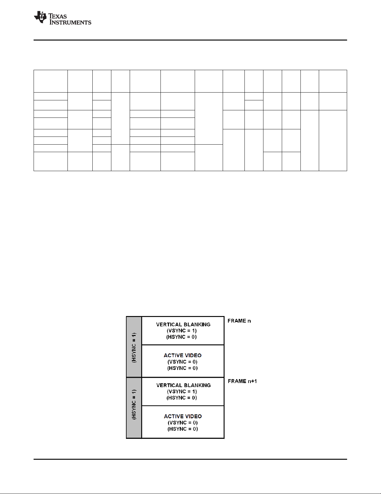
Figure 5 describes the horizontal and vertical blanking periods, and how they generally relate to the VSYNC and
HSYNC outputs. The SN65LVDS324 asserts VSYNC (driven high) by default, and drives VSYNC high for at
least one CLKOUT cycle at the beginning of each video frame. The SN65LVDS324 sensor interface logic
determines the beginning of an active video frame by sensor-dependent methods.
There may be certain VSYNC and HSYNC operating requirements in the video processing pipeline in the DSP,
such as a required number of vertical blanking lines, requirements for horizontal sync during vertical blanking, or
requirements for data patterns during blanking times, special requirements for still image capture, etc. Systems
that utilize SN65LVDS324 are required to configure the sensor to meet the vertical blanking and horizontal
blanking requirements set by DSP video processing pipeline; these limitations shall be met by the sensor and not
by SN65LVDS324 logic.
Figure 5. VSYNC and HSYNC Output Relation to Active Video Frames
Copyright © 2012, Texas Instruments Incorporated Submit Documentation Feedback 3
Product Folder Links: SN65LVDS324
Page 4
SN65LVDS324
SLLSED9 –NOVEMBER 2012
www.ti.com
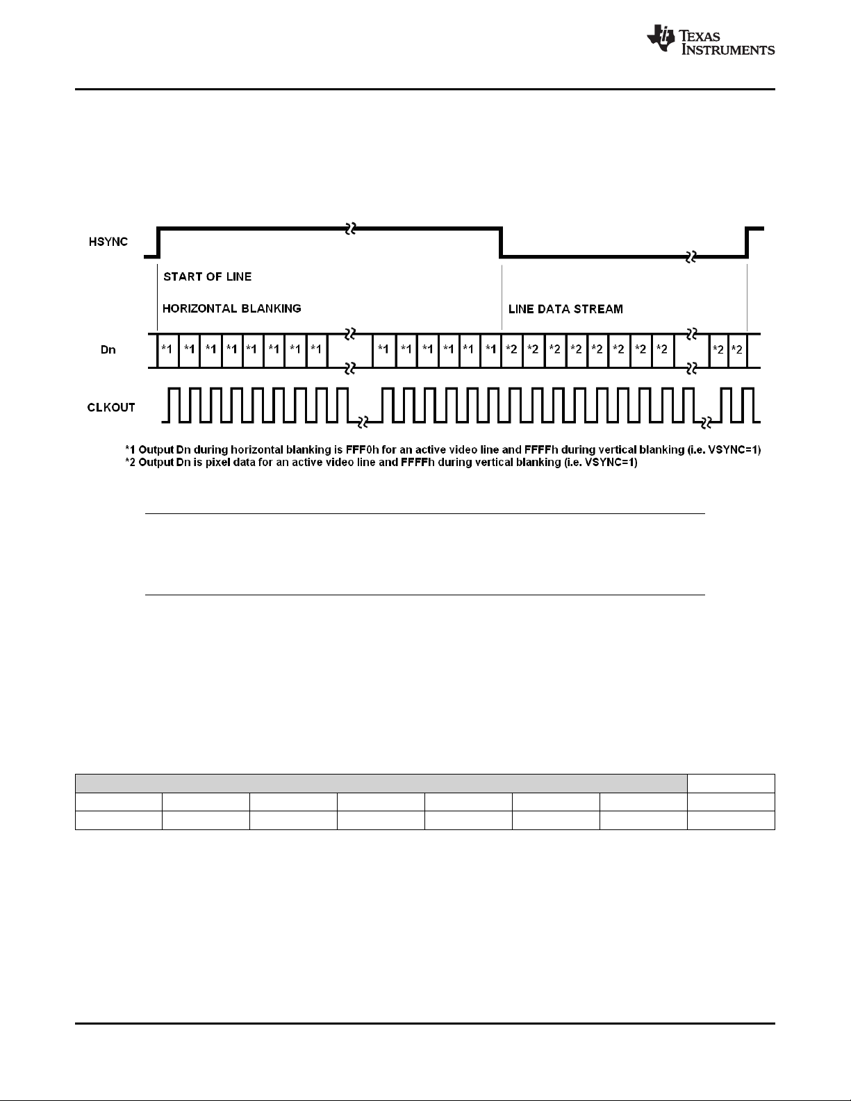
HSYNC is asserted (driven high) by default. HSYNC is driven low during the active video data stream transfer,
as illustrated in Figure 6. HSYNC may be de-asserted (driven low) while VSYNC is asserted or de-asserted.
As shown in Figure 6, the HSYNC output is generally asserted following an EOL (End of Line) indication from the
image sensor, and de-asserted (driven low) following a SOL (Start of Line) indication. Figure 6 further illustrates
the data expected on the output interface during blanking periods.
Figure 6. HSYNC Output Relation to Line Data Stream
NOTE
The SN65LVDS324 overrides the fixed patterns illustrated in Figure 6 (FFF0h and FFFFh
as shown by notes *1 and *2) when line data is received from the sensor during blanking
periods.
Local I2C Interface Overview
The SCL and SDA terminals are used for I2C clock and I2C data, respectively. The SN65LVDS324 I2C interface
conforms to the two-wire serial interface defined by the I2C Bus Specification, Version 2.1 (January 2000), and
supports standard mode transfers up to 400 kbps.
The device address byte is the first byte received following the START condition from the master device. The 7
bit device address for SN65LVDS324 is factory preset to 7'b0101101 (0x2D). Table 2 clarifies the SN65LVDS324
target address.
Table 2. SN65LVDS324 I2C Target Address Description
SN65LVDS324 I2C TARGET Address
Bit 7 (MSB) Bit 6 Bit 5 Bit 4 Bit 3 Bit 2 Bit 1 Bit 0 (W/R)
0 1 0 1 1 0 1 0/1
(1) When ADDR=1, Address Cycle is 0x5A (Write) and 0x5B (Read)
The following procedure is followed to write to the SN65LVDS324 I2C registers:
1. The master initiates a write operation by generating a start condition (S), followed by the SN65LVDS324 7-bit
address and a zero-value "W/R" bit to indicate a write cycle.
2. The SN65LVDS324 acknowledges the address cycle.
3. The master presents the sub-address (I2C register within SN65LVDS324) to be written, consisting of one
byte of data, MSB-first.
4. The SN65LVDS324 acknowledges the sub-address cycle.
5. The master presents the first byte of data to be written to the I2C register.
(1)
4 Submit Documentation Feedback Copyright © 2012, Texas Instruments Incorporated
Product Folder Links: SN65LVDS324
Page 5
SN65LVDS324
www.ti.com
SLLSED9 –NOVEMBER 2012
6. The SN65LVDS324 acknowledges the byte transfer.
7. The master may continue presenting additional bytes of data to be written, with each byte transfer completing
with an acknowledge from the SN65LVDS324.
8. The master terminates the write operation by generating a stop condition (P).
The following procedure is followed to read the SN65LVDS324 I2C registers:
1. The master initiates a read operation by generating a start condition (S), followed by the SN65LVDS324 7-bit
address and a one-value "W/R" bit to indicate a read cycle.
2. The SN65LVDS324 acknowledges the address cycle.
3. The SN65LVDS324 transmit the contents of the memory registers MSB-first starting at the last address
specified.
4. The SN65LVDS324 will wait for either an acknowledge (ACK) or a not-acknowledge (NACK) from the master
after each byte transfer; the I2C master acknowledges reception of each data byte transfer.
5. If an ACK is received, the SN65LVDS324 transmits the next byte of data.
6. The master terminates the read operation by generating a stop condition (P).
Control and Status Registers Overview
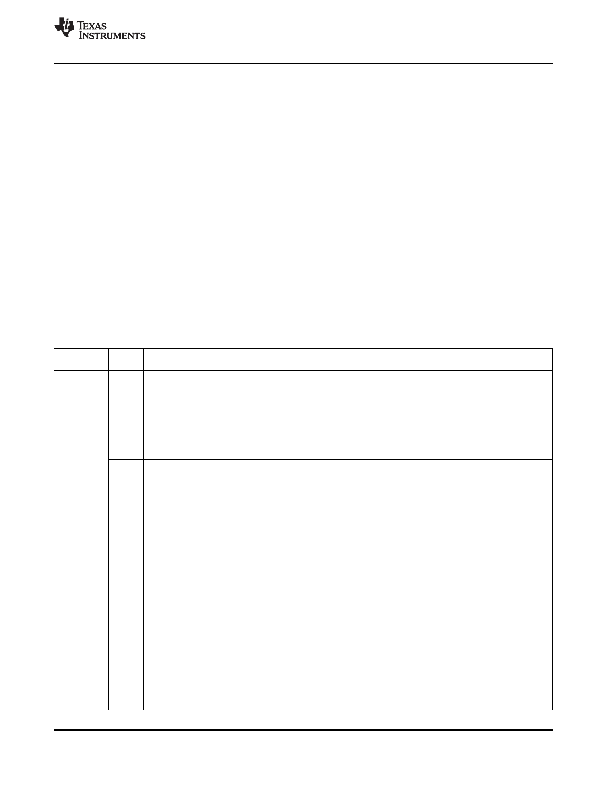
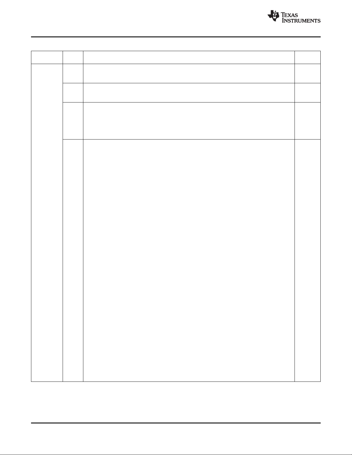
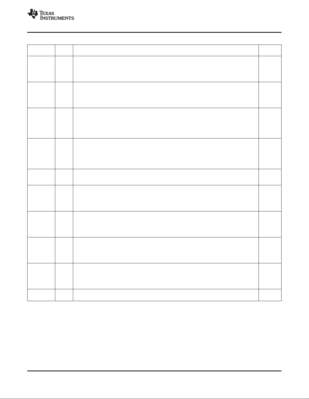
CSR's are accessible through the local I2C interface. Refer to Table 3 for SN65LVDS324 CSR descriptions.
Reads from reserved fields not described return zeros, and writes are ignored.
CSR's "SENSOR_CFG" and "PLL_CFG" must be set before the input clock (SCLK) is applied.
Table 3. SN65LVDS324 CSR Bit Field Definitions
ADDRESS BIT(S) DESCRIPTION
DEVICE_ID
0x00 – 0x07 7:0 Returns a string of ASCII characters "LVDS324" preceded by one space character. R
Addresses 0x00 - 0x07 = {0x20, 0x4C, 0x56, 0x44, 0x53, 0x33, 0x32, 0x34}
0x08 7:0 R
0x09
DEVICE_REV
Device revision; returns 0x01
SOFT_RESET
7 RW
This bit automatically clears when set to '1' and returns zeros when read. When set, the device is
reset to the default condition.
TESTMODE_VIDEO
When enabled, the device outputs a known color pattern with SCLK applied. The pattern is 128 lines
of red, 128 of green, and 128 of blue, repeated. CSR addresses 0B, 0C, 0D, and 0E set the active
image area, while addresses 1F, 20, 21, and 22 set the entire frame including blanking.
SENSOR_CFG and PLL_CFG control the bpp, PLL multiplier, and PLL range. The CLKOUT
6 RW
frequency directly scales the frame rate; for the default 2250x1100 frame, a CLKOUT frequency of
148.5MHz causes 60fps.
0 – Disabled (default)
1 – Enabled
LSB_FIRST_OUTPUT
5 0 – Output data is MSB first; D[15:0] output represents MSB at D0 RW
1 – Output data is LSB first; D[15:0] output represents LSB at D0 (default)
SYNC_ACTIVE_HIGH
4 0 – VSYNC and HSYNC are output low during blanking periods RW
1 – VSYNC and HSYNC are output high during blanking periods (default)
CLK_CENTERED_TIMING
3 0 – Output timing accommodates long setup time receivers [e.g. DaVinci] (default) RW
1 – Outputs are clock-centered for relatively matched setup/hold receivers [e.g. OMAP]
SENSOR_CFG
This field shall be written to configure the sensor interface per Table 1.
000 – LVDS Parallel 10bpp mode (default) 100 – 1-Channel 4-Lane 12bpp mode
2:0 RW
001 – LVDS Parallel 12bpp mode 101 – 1-Channel 4-Lane 14bpp mode
010 – 2-Channel 2-Port 12bpp mode 110 – 1-Channel 4-Lane 16bpp mode
011 – 2-Channel 2-Port 16bpp mode 111 – 1-Channel 2-Lane 12bpp mode
ACCESS
(1)
(1) R = Read Only; RW = Read/Write (only reads return undetermined values)
Copyright © 2012, Texas Instruments Incorporated Submit Documentation Feedback 5
Product Folder Links: SN65LVDS324
Page 6
SN65LVDS324
SLLSED9 –NOVEMBER 2012
Table 3. SN65LVDS324 CSR Bit Field Definitions (continued)
ADDRESS BIT(S) DESCRIPTION
CLKOUT_PLL_LOCK
7 0 – Output pixel clock PLL not locked R
1 – Output pixel clock PLL locked
VCM_MODE
6 0 – Selects Low common mode voltage range RW
1 – Selects High common mode voltage range (default)
D_SLEW_RATE
Controls the rise and fall time for D[15:0].
00 – Slowest; sets to 50% of the baseline speed
5:4 RW
01 – Slower; sets to 75% of the baseline speed
10 – Baseline (default)
11 – Fastest; sets to 150% of the baseline speed
PLL_CFG
This field sets the allowable SCLK frequency range, based on the mode set by SENSOR_CFG. The
register defaults to 10 (and 01 for the 14bpp mode).
spacer
LVDS Parallel 10/12bpp (PLL Multiplier = 2)
00 – SCLK = 18.5 to 33MHz, CLKOUT = 37 to 66MHz
01 – SCLK = 31 to 60MHz, CLKOUT = 62 to 120MHz
10 – SCLK = 58 to 81MHz, CLKOUT = 116 to 162MHz
11 – Reserved
spacer
2-Channel 2-Port 12bpp and 1-Channel 4-Lane 12bpp (PLL Multiplier = 2/3)
0x0A
00 – SCLK = 55.5 to 99MHz, CLKOUT = 37 to 66MHz
01 – SCLK = 97 to 180MHz, CLKOUT = 64.7 to 120MHz
10 – SCLK = 178 to 243MHz, CLKOUT = 118.7 to 162MHz
11 – Reserved
spacer
2-Channel 2-Port 16bpp and 1-Channel 4-Lane 16bpp (PLL Multiplier = 1/2)
1:0 RW
00 – SCLK = 74 to 120MHz, CLKOUT = 37 to 60MHz
01 – SCLK = 118 to 180MHz, CLKOUT = 59 to 90MHz
10 – SCLK = 178 to 222MHz, CLKOUT = 89 to 111MHz
11 – SCLK = 220 to 324MHz, CLKOUT = 110 to 162MHz
spacer
1-Channel 4-Lane 14bpp (PLL Multiplier = 4/7)
00 – SCLK = 120 to 220MHz, CLKOUT = 68.6 to 125.7MHz
01 – SCLK = 218 to 283.5MHz, CLKOUT = 124.6 to 162MHz
10 – Reserved
11 – Reserved
spacer
1-Channel 2-Lane 12bpp (PLL Multiplier = 1/3)
00 – SCLK = 55.5 to 99MHz, CLKOUT = 18.5 to 33MHz
01 – SCLK = 97 to 180MHz, CLKOUT = 32.3 to 60MHz
10 – SCLK = 178 to 297MHz, CLKOUT = 59.3 to 99MHz
11 – Reserved
www.ti.com
ACCESS
(1)
6 Submit Documentation Feedback Copyright © 2012, Texas Instruments Incorporated
Product Folder Links: SN65LVDS324
Page 7
SN65LVDS324
www.ti.com
SLLSED9 –NOVEMBER 2012
Table 3. SN65LVDS324 CSR Bit Field Definitions (continued)
ADDRESS BIT(S) DESCRIPTION
FRAME_WIDTH_MSB
0x0B 4:0 field's default is 0x07. The max width is 8191. RW
0x0C 7:0 field's default is 0x80. The max width is 8191. RW
0x0D 4:0 RW
0x0E 7:0 RW
0x0F – 0x1E 7:0 RW
0x1F 4:0 controls the high order byte of the frame width including blanking; the default is 2250 (0x08CA), and RW
0x20 7:0 controls the low order byte of the frame width including blanking; the default is 2250 (0x08CA), and RW
0x21 4:0 controls the high order byte of the frame height including blanking; the default is 1100 (0x044C), and RW
0x22 7:0 controls the low order byte of the frame height including blanking; the default is 1100 (0x044C), and RW
0x23 – 0x30 7:0 RW
The width of the active area; this field is the high order byte. The default is 1920 (0x0780), and this
When TESTMODE_VIDEO is disabled, this field is only used to set SENSOR_SPECIFIC registers
that flag window size errors.
FRAME_WIDTH_LSB
The width of the active area; this field is the low order byte. The default is 1920 (0x0780), and this
When TESTMODE_VIDEO is disabled, this field is only used to set SENSOR_SPECIFIC registers
that flag window size errors.
FRAME_HEIGHT_MSB
The height of the active area; this field is the high order byte. The default is 1080 (0x0438), and this
field's default is 0x04. The max height is 8191.
When TESTMODE_VIDEO is disabled, this field is only used to set SENSOR_SPECIFIC registers
that flag window size errors. In LVDS Parallel modes, the height must include all lines between SAVValid and EAV-Valid.
FRAME_HEIGHT_LSB
The height of the active area; this field is the low order byte. The default is 1080 (0x0438), and this
field's default is 0x38. The max height is 8191.
When TESTMODE_VIDEO is disabled, this field is only used to set SENSOR_SPECIFIC registers
that flag window size errors. In LVDS Parallel modes, the height must include all lines between SAVValid and EAV-Valid.
SENSOR_SPECIFIC
These are sensor-specific status registers, and depend on SENSOR_CFG. They are further
described by Table 4 through Table 6.
TESTMODE_WIDTH_MSB
Applies only when TESTMODE_VIDEO is enabled, and configurable up to 8191 pixels. This field
this field's default is 0x08.
For 720p, a width of 1500 (0x05DC) facilitates 60fps with 74.25MHz.
TESTMODE_WIDTH_LSB
Applies only when TESTMODE_VIDEO is enabled, and configurable up to 8191 pixels. This field
this field's default is 0xCA.
For 720p, a width of 1500 (0x05DC) facilitates 60fps with 74.25MHz.
TESTMODE_HEIGHT_MSB
Applies only when TESTMODE_VIDEO is enabled, and configurable up to 8191 pixels. This field
this field's default is 0x04.
For 720p, a height of 825 (0x0339) facilitates 60fps with 74.25MHz.
TESTMODE_ HEIGHT_LSB
Applies only when TESTMODE_VIDEO is enabled, and configurable up to 8191 pixels. This field
this field's default is 0x4C.
For 720p, a height of 825 (0x0339) facilitates 60fps with 74.25MHz.
RESERVED
These registers are reserved for factory test. Do not write to them.
ACCESS
(1)
Copyright © 2012, Texas Instruments Incorporated Submit Documentation Feedback 7
Product Folder Links: SN65LVDS324
Page 8
SN65LVDS324
SLLSED9 –NOVEMBER 2012
www.ti.com
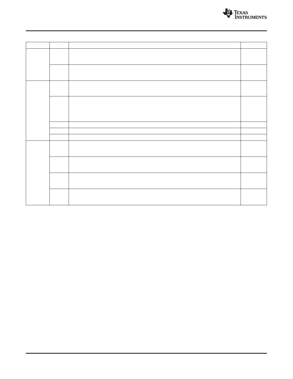
Table 4. Sensor-Specific Registers for Aptina Modes
ADDRESS BIT(S) DESCRIPTION ACCESS
FILLER_EN
6 0 – FLR codes are not used in data stream RW
0x0F
0x10
0x11
(1) R = Read Only; RW = Read/Write; W = Write Only (reads return undetermined values)
1 – FLR codes are used in data stream (default)
CRC_EN
5 0 – CRC is not used in the data stream RW
1 – CRC is used in the data stream (default)
CLEAR_STATUS
7 W
When a '1' is written to this field, the status bits in 0x10 and 0x11 are cleared, and this bit is autocleared to a zero value (always returns zero when read)
CRC_ERR_LANE3
0 – No checksum error detected (default)
3 R
1 – Checksum error detected
Note: Bits in registers 0x10 and 0x11 are latched and cleared only when the CLEAR_STATUS field
is written.
2 CRC_ERR_LANE2; same bit function as CRC_ERR_LANE3 but applied to LANE 2. R
1 CRC_ERR_LANE1; same bit function as CRC_ERR_LANE3 but applied to LANE 1. R
0 CRC_ERR_LANE0; same bit function as CRC_ERR_LANE3 but applied to LANE 0. R
UNKNOWN_SYNC_CODE
5 0 – No unexpected sync code (default) R
1 – Sync code (final word of sync_code) does not match a defined type
SOF_ERR
4 0 – No SOF error occurred (default) R
1 – SOF was detected when it was unexpected
SOL_ERR
3 0 – No SOL error occurred (default) R
1 – SOL was detected when it was unexpected
SOV_ERR
2 0 – No SOV error occurred (default) R
1 – SOV was detected when it was unexpected
(1)
8 Submit Documentation Feedback Copyright © 2012, Texas Instruments Incorporated
Product Folder Links: SN65LVDS324
Page 9
SN65LVDS324
www.ti.com
SLLSED9 –NOVEMBER 2012
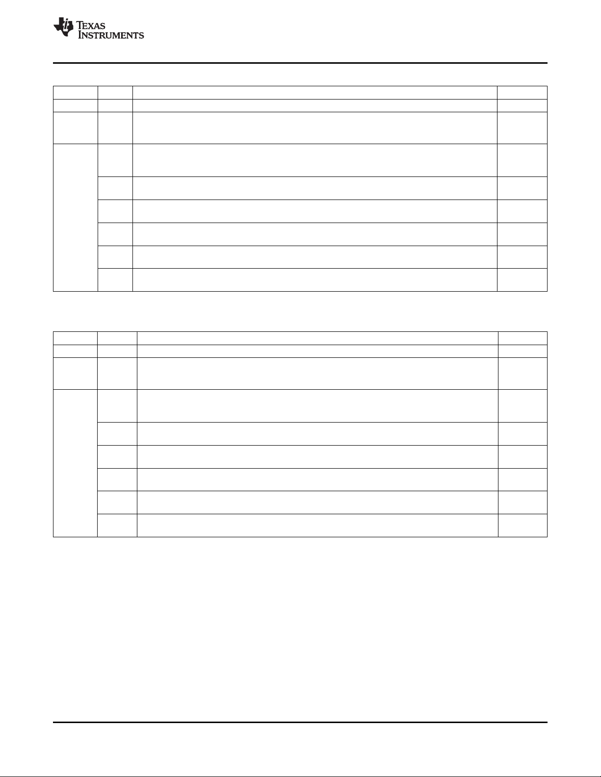
Table 5. Sensor-Specific Registers for Panasonic Modes
ADDRESS BIT(S) DESCRIPTION ACCESS
0x0F 7:0 Reserved. R
0x10 7 W
0x11
(1) R = Read Only; W = Write Only
CLEAR_STATUS
When a '1' is written to this field, the status bits in 0x11 are cleared, and this bit is auto-cleared to a
zero value (always returns zero when read)
FRAME_SIZE_ERROR
7 0 – Start up sequence has not identified a frame size error, decode window applied. R
1 – Start up sequence identified a frame size error, decode window is not applied
UNKNOWN_SYNC_CODE
5 R
When set to'1', sync code (final word of sync_code) does not match a defined type
SOF_ERR
4 R
When set to '1', SOF was detected when it was unexpected per the decode window.
SOL_ERR
3 R
When set to '1', SOL was detected when it was unexpected per the decode window.
EOF_ERR
1 R
When set to '1', EOF was detected when it was unexpected per the decode window.
EOL_ERR
0 R
When set to '1', EOL was detected when it was unexpected per the decode window.
Table 6. Sensor-Specific Registers for Sony Modes
ADDRESS BIT(S) DESCRIPTION ACCESS
0x0F 7:0 Reserved. R
0x10 7 W
0x11
(1) R = Read Only; W = Write Only (reads return undetermined values)
CLEAR_STATUS
When a '1' is written to this field, the status bits in 0x11 are cleared, and this bit is auto-cleared to a
zero value (always returns zero when read)
FRAME_SIZE_ERROR
7 0 – Start up sequence has not identified a frame size error, decode window applied. R
1 – Start up sequence identified a frame size error, decode window is not applied
UNKNOWN_SYNC_CODE
5 R
When set to '1', sync code (final word of sync_code) does not match a defined type
SAV_VALID_ERR
4 R
When set to '1', SAV (Valid Line) was unexpectedly detected per the decode window.
SAV_INVALID_ERR
3 R
When set to '1', SAV (Invalid Line) was unexpectedly detected per the decode window.
EAV_VALID_ERR
1 R
When set to '1', EAV (Valid Line) was unexpectedly detected per the decode window.
EAV_INVALID_ERR
0 R
When set to '1', EAV (Invalid Line) was unexpectedly detected per the decode window.
(1)
(1)
Copyright © 2012, Texas Instruments Incorporated Submit Documentation Feedback 9
Product Folder Links: SN65LVDS324
Page 10
A
B
C
D
E
F
G
H
J
K
1
2
3
4
5
6
SCLKN
SD2N
SD0N
SD3N
SD4N
SD5N
SCLKP
SD2P
SD0P
SD3P
SD4P
SD5P
VCCA
VCCA
HSYNC
GND
GNDA
VCC
GNDA
D13
D11
D9
D7
D5
D3
VCCA
D12
D10
D8
D6
D4
D2
CLKOUT
SD1N SD1P
SCL VSYNC D14
RST#
SD7P SD8P
SD7N
SD9P
SD8N
SD10P
SD9N
SD11P
SD10N SD11N
VCC
GNDA
GND
GND
SD6P
SD6N
SDA
D15
D1 D0
SN65LVDS324
SLLSED9 –NOVEMBER 2012
www.ti.com
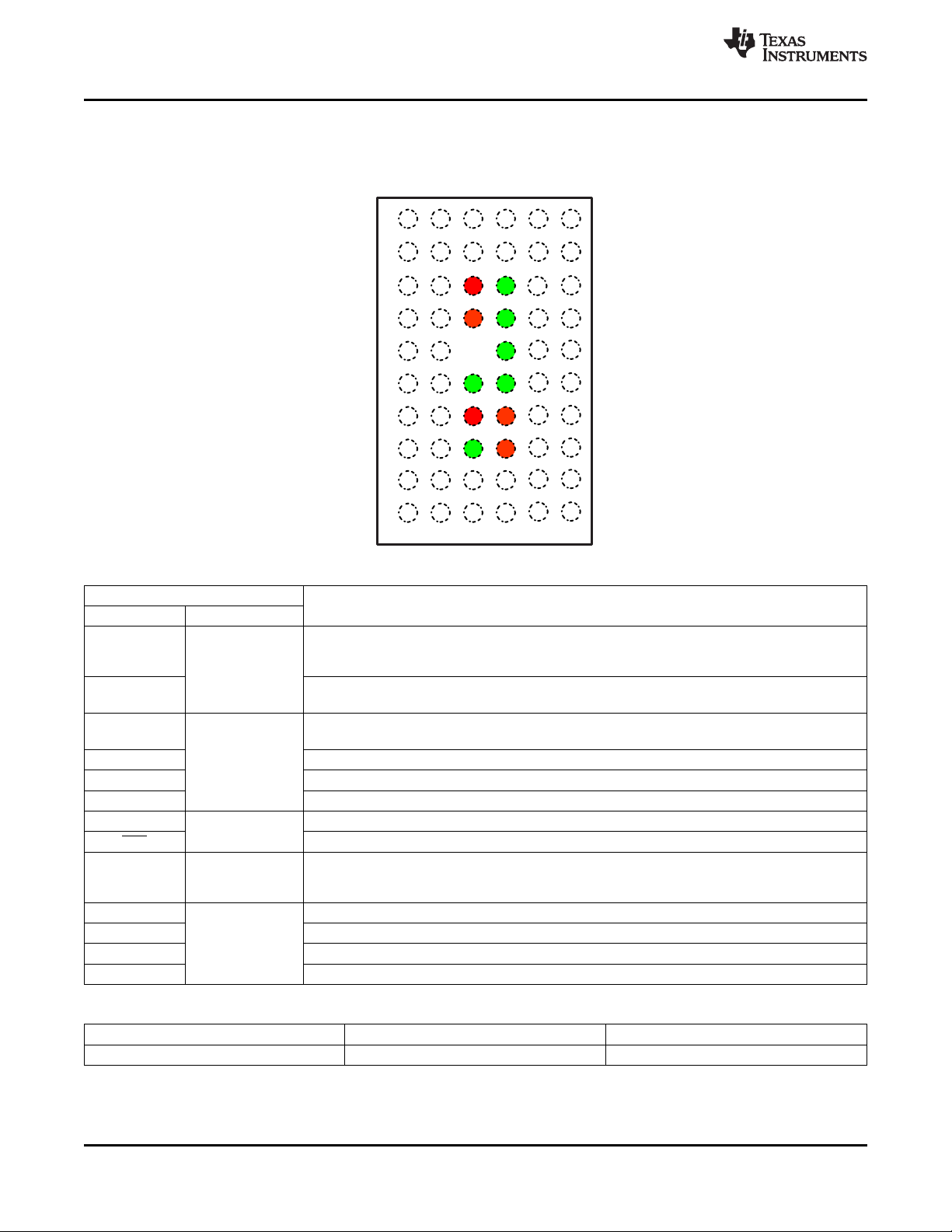
ZQL PACKAGE
(TOP VIEW)
PIN FUNCTIONS
PIN
SIGNAL I/O
SubLVDS Input Data Lanes with 100Ω differential termination. In the 2-Channel 2-Port
SD[11:0]P/N
SubLVDS Input
(Failsafe)
SCLKP/N
D[15:0]
CLKOUT Parallel Output Clock.
CMOS Output
configurations, SD2P/N is used as Channel 2 clock.
See Table 1 for sensor SubLVDS signal mapping per configuration.
SubLVDS Input Clock.
In 2-Channel 2-Port mode, this input is the Channel 1 clock.
Parallel Output Pixel Data.
Pixel data outputs beyond the pixel data width configuration are driven low.
HSYNC Parallel Output Horizontal Sync.
VSYNC Parallel Output Vertical Sync.
SCL CMOS Input Local I2C Programming Interface Clock Signal.
Input/Output
(Failsafe)
CMOS
RST Logic Reset. Active when Low.
SDA Local I2C Programming Interface Data Signal.
(Failsafe)
GNDA Reference Ground for Analog Circuits.
VCCA 1.8V Power Supply for Analog Circuits.
GND Reference Ground for Digital Circuits.
VCC 1.8V Power Supply for Digital Circuits.
Power Supply
ORDERING INFORMATION
PART NUMBER PART MARKING PACKAGE / SHIPPING
(1) For the most current package and ordering information, see the TI web site at www.ti.com.
10 Submit Documentation Feedback Copyright © 2012, Texas Instruments Incorporated
Product Folder Links: SN65LVDS324
SN65LVDS324ZQLR LVDS324 59-ball PBGA / Reel
DESCRIPTION
(1)
Page 11
SN65LVDS324
www.ti.com
SLLSED9 –NOVEMBER 2012
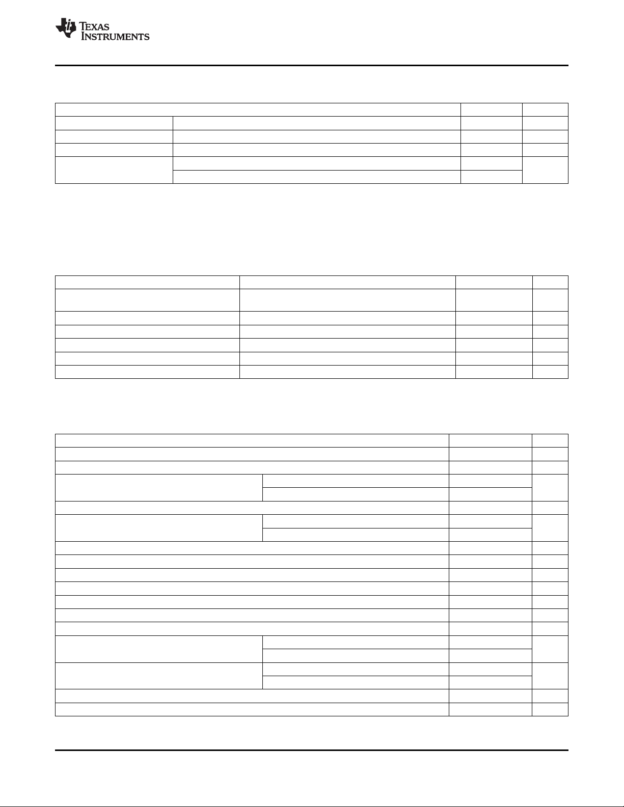
ABSOLUTE MAXIMUM RATINGS
over operating free-air temperature range (unless otherwise noted)
Supply Voltage Range V
Input Voltage Range All Input Terminals –0.5 to 2.175 V
Storage temperature T
Electrostatic discharge kV
(1) Stresses beyond those listed under absolute maximum ratings may cause permanent damage to the device. These are stress ratings
only and functional operation of the device at these or any conditions beyond those indicated under recommended operating conditions
is not implied. Exposure to absolute-maximum-rated conditions for extended periods may affect device reliability.
(2) Tested in accordance with JEDEC Standard 22, Test Method A114-B
(3) Tested in accordance with JEDEC Standard 22, Test Method C101-A
, V
CCA
CC
S
Human Body Model
Charged-device model
(2)
(3)
(1)
VALUE UNITS
–0.3 to 2.175 V
–65 to 150 °C
±4
±1.5
THERMAL CHARACTERISTICS
over operating free-air temperature range (unless otherwise noted)
PARAMETER TEST CONDITIONS MIN TYP MAX UNIT
θ
Junction-to-free-air thermal resistance 73.9 °C/W
JA
θ
Junction-to-case-top thermal resistance Cu cold plate measurement process 30.6 °C/W
JCT
θ
Junction-to-board thermal resistance EIA/JESD 51-8 37.7 °C/W
JB
ψ
Junction-to-top of package EIA/JESD 51-2 1.3 °C/W
JT
ψ
Junction-to-board EIA/JESD 51-6 36.9 °C/W
JB
T
Junction temperature 125 °C
J
(1) For more information about traditional and new thermal metrics, see the IC Package Thermal Metrics application report, SPRA953.
High-K JEDEC test board, 2s2p (double signal layer,
double buried power plane), no air flow
(1)
RECOMMENDED OPERATING CONDITIONS
over operating free-air temperature range (unless otherwise noted)
MIN NOM MAX UNIT
V
CCA
V
CC
V
CCn(PP)
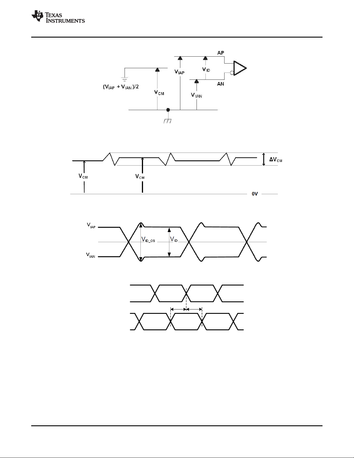
|VID| Magnitude of differential input voltage; see Figure 7 90 350 mV
V
CM
V
CM
V
IN_DC
V
ID_OS
T
A
T
CASE
f
I2C
f
CLK
t
SETUP
t
HOLD
t
DUTCLK
C
L
(1) The SN65LVDS324 supports up to 10pF parallel output load capacitance under test conditions.
Power supply; analog circuits 1.65 1.8 1.95 V
Power supply; digital circuits 1.65 1.8 1.95 V
f
< 1MHz 100
Power supply voltage noise mV
Input common mode voltage; see Figure 7 mV
NOISE
f
> 1MHz 40
NOISE
CSR 0A[6] = 0 100 650
CSR 0A[6] = 1 550 1200
Peak to peak input common mode voltage variation; see Figure 8 50 mV
SubLVDS receiver input voltage range 1400 mV
Differential input voltage overshoot/undershoot; see Figure 9 20%
Operating free-air temperature –40 85 °C
Case temperature 101 °C
Local I2C interface operating frequency 400 kHz
SubLVDS input clock (SCLKP/N) frequency 18.5 324 MHz
SubLVDS data setup time to SCLKP/N
transition; see Figure 10
SubLVDS data hold time after SCLKP/N
transition; see Figure 10
LVDS Parallel modes 1500
All other modes 350
LVDS Parallel modes 1500
All other modes 350
SubLVDS CLK input clock duty cycle 45% 55%
Parallel output load capacitance
(1)
5 6 pF
ps
ps
Copyright © 2012, Texas Instruments Incorporated Submit Documentation Feedback 11
Product Folder Links: SN65LVDS324
Page 12
SN65LVDS324
SLLSED9 –NOVEMBER 2012
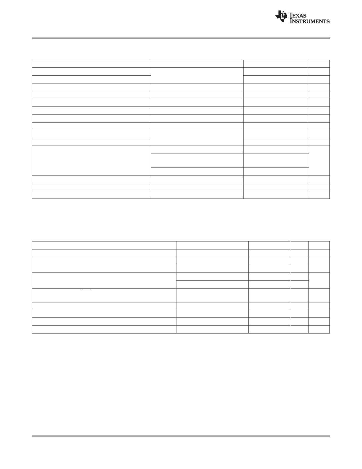
DC ELECTRICAL CHARACTERISTICS
over operating free-air temperature range (unless otherwise noted)
PARAMETER TEST CONDITIONS MIN TYP
V
THL
V
THH
V
IL
V
IH
V
OH
V
OL
I
OS
I
LEAK
I
IH
I
IL
I
CC
R
DIFF
R
RST
C
IN
(1) All typical values are at VCC= 1.8V and TA= 25°C
(2) VCC= 1.95V; TA= 0°C; CL= 6pF; Worst case test pattern
(3) VCC= 1.8V; TA= 25°C; CL= 5pF; Typical power test pattern
Low-level differential input voltage threshold –40 mV
High-level differential input voltage threshold 40 mV
V
SD[11:0]P
– V
SD[11:0]N
Low-level control signal input voltage SCL, SDA 0.3×V
High-level control signal input voltage SCL, SDA 0.7×V
High-level output voltage IOH= –2 mA 1.3 V
Low-level output voltage IOL= 2 mA 0.4 V
Short circuit output current Output VOHdriving GND short –35 mA
Failsafe input leakage current VCC= 0; V
High level input current 5 µA
Low level input current 5 µA
SDA, SCL
CC(PIN)
LVDS Parallel 1080p60 89 125
Active current
(2) (3)
2-Channel 2-Port 1080p60
1-Channel 4-Lane 1080p60
1-Channel 2-Lane 720p60 74 100
Differential termination resistance 80 100 125 Ω
Reset input resistance 120 150 180 kΩ
Input pin capacitance 1.5 pF
www.ti.com
(1)
MAX UNIT
, V
SCLKP
– V
SCLKN
CC
CC
=1.8 V 10 µA
83 120 mA
V
V
SWITCHING CHARACTERISTICS
over recommended operating conditions (unless otherwise noted)
PARAMETER TEST CONDITIONS MIN TYP
F
CLKOUT
t
del
t
pd
t
en
t
r
t
f
t
dc
t
j
(1) All typical values are at VCC= 1.8V and TA= 25°C.
CLKOUT frequency CL= 6 pF 18.5 162 MHz
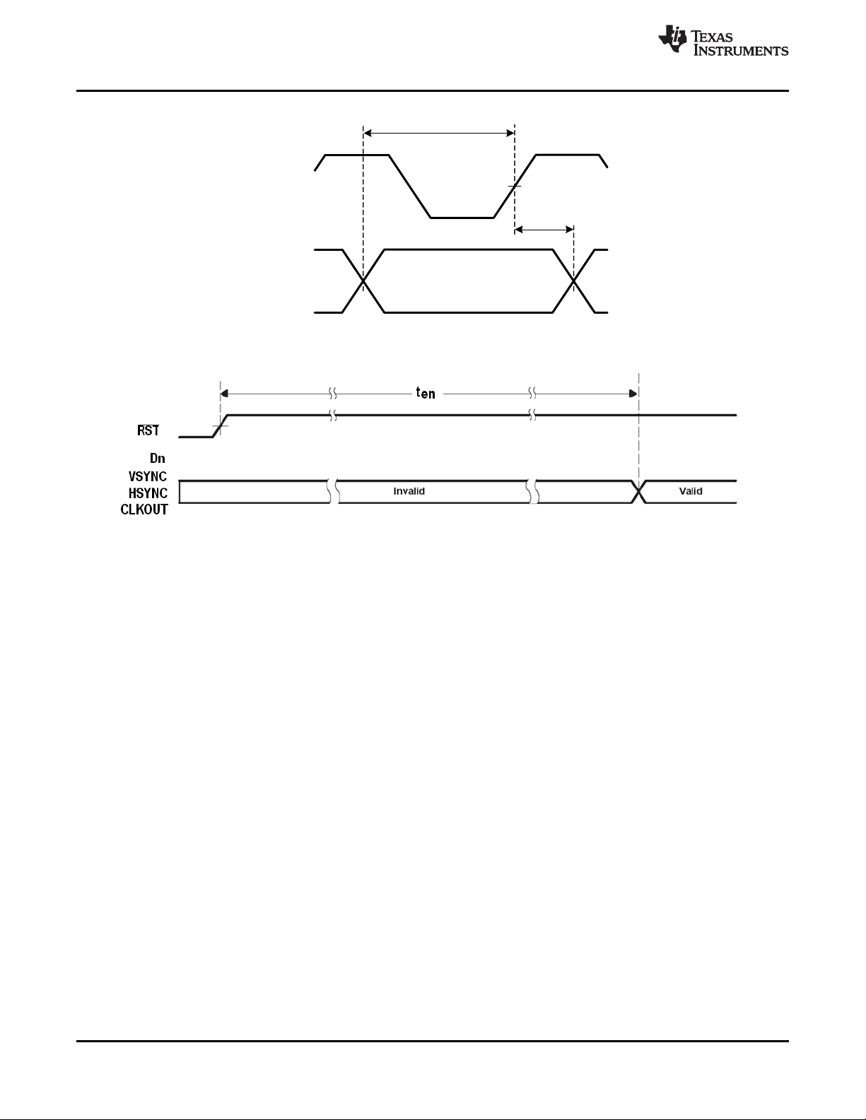
Data valid to CLKOUT↑ (see Figure 11) ns
CLKOUT↑ to data switching (see Figure 11) ns
Enable time, RST ↑ to output valid and CLKOUT meets
electrical specifications
CL= 6 pF; CSR 09[3] = 1 1.5
CL= 6 pF; CSR 09[3] = 0 3.8
CL= 6 pF; CSR 09[3] = 1 1.5
CL= 6 pF; CSR 09[3] = 0 0.2
F
CLKOUT
See Figure 12
Rise transition time, output (20% to 80%) CL= 6 pF, CSR 0A[5:4] = 10 450 750 1300 ps
Fall transition time, output (80% to 20%) CL= 6 pF, CSR 0A[5:4] = 10 450 750 1300
CLKOUT duty cycle 45% 55%
CLKOUT residual jitter Peak to peak 370 ps
= 148.5 MHz,
(1)
MAX UNIT
2 ms
12 Submit Documentation Feedback Copyright © 2012, Texas Instruments Incorporated
Product Folder Links: SN65LVDS324
Page 13
SCLK
t
SETUP
t
HOLD
SD[0:11]
SN65LVDS324
www.ti.com
SLLSED9 –NOVEMBER 2012
Figure 7. SubLVDS Input Voltage Definitions
Figure 8. SubLVDS Delta Common Mode Input Voltage Definition
Figure 9. VIDOvershoot Definition
Figure 10. SubLVDS Timing Definitions
Copyright © 2012, Texas Instruments Incorporated Submit Documentation Feedback 13
Product Folder Links: SN65LVDS324
Page 14
D[15:0]
HSYNC
VSYNC
CLKOUT
t
del
t
pd
SN65LVDS324
SLLSED9 –NOVEMBER 2012
www.ti.com
Figure 11. CMOS Output Timing Waveforms
Figure 12. Device Enable Waveforms
14 Submit Documentation Feedback Copyright © 2012, Texas Instruments Incorporated
Product Folder Links: SN65LVDS324
Page 15
IMAGE
SENSOR
1080p60
Digital Signal
Processor
RST
D[15:10]
D[9:0]
CLKOUT
VSYNC
HSYNC
< 1cm difference in length
SN65LVDS324
SD[11:2]P
SD[11:2]N
SCLKP/N
SD[1:0]P/N
SCL
SDA
1.8V
VCC
VCCA
37.125 MHz
SDI
SCK
SDO
LVDS Parallel 10-Bit 1080p60
LVDS DDR @ 74.25MHz
CLKIN
D[11:2]_P
D[11:2]_N
CLK_P/N
3x 10Ω
CLKOUT = 148.5MHz
D[15:10] Output = 6’b0
DSP I/O @ 1.8V CMOS
NC
1.8V
1.5kΩ
Configuration and Control
CSR 09[2:0] = 3’b000
CSR 0A[1:0] = 2’b10
SN65LVDS324
www.ti.com
SLLSED9 –NOVEMBER 2012
TYPICAL APPLICATIONS
spacer
The SN65LVDS324 offers several operating modes, as described in this section. The typical mode of 1080p60
involves a 148.5MHz output clock.
The parallel output video interface provides up to 16-bits of data per pixel, a vertical synchronization signal
(VSYNC), and a horizontal synchronization signal (HSYNC) that are all synchronous to the output clock,
CLKOUT. VSYNC and HSYNC are by default logically active high, and output a high logic level during blanking
periods.
The following application diagrams illustrate each high-level typical configuration given in Table 1.
Sony LVDS Parallel 10-Bit Mode
Figure 13 illustrates the LVDS Parallel 10-bit mode for 1080p60 operation.
In this configuration, the image sensor transmits 10-bit video with a DDR reference clock operating at 74.25MHz.
The SN65LVDS324 provides a 2x PLL to convert the 74.25MHz SubLVDS input to a 148.5MHz pixel clock
output (CLKOUT) for the 10-bit output interface.
An SPI-like serial bus is used to configure and control the sensor in this typical application example. The DSP
shall properly configure the sensor to the particular target application, which may involve setting the electrical
interface and optical gain settings.
The SN65LVDS324 identifies sync codes from the data stream to identify vertical and horizontal sync conditions,
and sets the outputs HSYNC and VSYNC appropriately.
Copyright © 2012, Texas Instruments Incorporated Submit Documentation Feedback 15
Figure 13. LVDS Parallel 10bpp Application
Product Folder Links: SN65LVDS324
Page 16
IMAGE
SENSOR
1080p60
SN65LVDS324
SD[1:0]P/N
SD[4:3]P/N
SCLKP/N
SD2P/N
SD[11:5]P/N
SCL
SDA
1.8V
VCC
VCCA
CLKIN
CH1[1:0]_P/N
CH2[1:0]_P/N
CLK1_P/N
CLK2_P/N
Configuration
and Control
CSR 09[2:0] = 3’b010
CSR 0A[1:0] = 2’b10
Digital Signal
Processor
D[15:12]
D[11:0]
CLKOUT
VSYNC
HSYNC
CLKOUT = 148.5MHz
D[15:12] Output = 4’b0
DSP I/O @ 1.8V CMOS
NC
1.8V
< 1cm difference in length
RST
1.5k Ω
2-Channel 2-Port
12-Bit 1080p60
LVDS DDR @ 222.75MHz
SDI
SCK
SDO
37.125 MHz
IMAGE
SENSOR
1080p60
Digital Signal
Processor
RST
D[15:12]
D[11:0]
CLKOUT
VSYNC
HSYNC
< 1cm difference in length
SN65LVDS324
SD[11:0]P
SD[11:0]N
SCLKP/N
SD[1:0]P/N
SCL
SDA
1.8V
VCC
VCCA
37.125 MHz
SDI
SCK
SDO
LVDS Parallel 12-Bit 1080p60
LVDS DDR @ 74.25MHz
CLKIN
D[11:0]_P
D[11:0]_N
CLK_P/N
3x 10Ω
CLKOUT = 148.5MHz
D[15:12] Output = 4’b0
DSP I/O @ 1.8V CMOS
NC
1.8V
1.5kΩ
Configuration and Control
CSR 09[2:0] = 3’b001
CSR 0A[1:0] = 2’b10
SN65LVDS324
SLLSED9 –NOVEMBER 2012
www.ti.com
TYPICAL APPLICATIONS (continued)
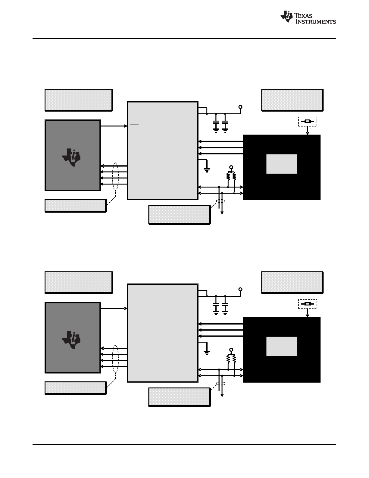
Sony LVDS Parallel 12-Bit Mode
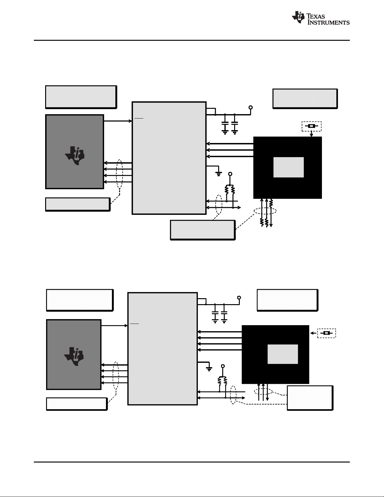
Figure 14 illustrates the 12-bit LVDS Parallel mode for 1080p60 operation. This mode operates identically to the
LVDS Parallel 10-bit mode other than the data width and sync codes.
Panasonic 2-Channel 2-Port 12-Bit Mode
Figure 15 illustrates the 1080p60 2-Channel 2-Port 12-bit operating mode.
The channel 2 clock is not guaranteed to be synchronous with channel 1; the SN65LVDS324 Word Alignment
function provides the data synchronization between channel 1 and channel 2. If the sensor output is dual-frame
WDR, the SN65LVDS324 transmits the data for both frames.
16 Submit Documentation Feedback Copyright © 2012, Texas Instruments Incorporated
Figure 14. LVDS Parallel 12bpp Application
Figure 15. 2-Channel 2-Port 12bpp Application
Product Folder Links: SN65LVDS324
Page 17
1080p60
IMAGE
SENSOR
SN65LVDS324
SD[3:0]P
SD[3:0]N
SCLKP/N
SD[11:4]P/N
SCL
SDA
1.8V
VCC
VCCA
27MHz
SCL
SDA
CLKIN
SLVS[3:0]_P
SLVS[3:0]_N
SLVSC_P/N
2x
1.5k Ω
1.8V
Digital Signal
Processor
D[15:12]
D[11:0]
CLKOUT
VSYNC
HSYNC
CLKOUT = 148.5MHz
D[15:12] Output = 4’b0
DSP I/O @ 1.8V CMOS
NC
< 1cm difference in length
Configuration and Control
CSR 09[2:0] = 3’b100
CSR 0A[1:0] = 2’b10
RST
1-Channel 4-Lane
12-Bit 1080p60
LVDS DDR @ 222.75MHz
IMAGE
SENSOR
1080p60
SN65LVDS324
SD[1:0]P/N
SD[4:3]P/N
SCLKP/N
SD2P/N
SD[11:5]P/N
SCL
SDA
1.8V
VCC
VCCA
CLKIN
CH1[1:0]_P/N
CH2[1:0]_P/N
CLK1_P/N
CLK2_P/N
Configuration
and Control
CSR 09[2:0] = 3’b011
CSR 0A[1:0] = 2’b11
Digital Signal
Processor
D[15:0]
CLKOUT
VSYNC
HSYNC
CLKOUT = 148.5MHz
DSP I/O @ 1.8V CMOS
1.8V
< 1cm difference in length
RST
1.5k Ω
2-Channel 2-Port
16-Bit 1080p60
LVDS DDR @ 297MHz
SDI
SCK
SDO
37.125 MHz
SN65LVDS324
www.ti.com
TYPICAL APPLICATIONS (continued)
Panasonic 2-Channel 2-Port 16-bit Mode
Figure 16 illustrates the 16-bit color 1080p60 2-Channel 2-Port operating mode.
Figure 16. 2-Channel 2-Port 16bpp Application
SLLSED9 –NOVEMBER 2012
Aptina 1-Channel 4-Lane 12-bit Mode
Figure 17 illustrates the 1080p60 1-Channel 4-Lane 12-bit per pixel operating mode with an image sensor pixel
clock frequency is 148.5MHz (222.75MHz SubLVDS clock frequency). In this configuration, the SN65LVDS324
outputs the parallel pixel clock (CLKOUT) at 148.5MHz by implementing a PLL operating with a 2/3 multiplier
from the SubLVDS clock input (SCLKP/N).
Copyright © 2012, Texas Instruments Incorporated Submit Documentation Feedback 17
Figure 17. 1-Channel 4-Lane 12bpp Application
Product Folder Links: SN65LVDS324
Page 18
1080p60
IMAGE
SENSOR
SN65LVDS324
SD[3:0]P
SD[3:0]N
SCLKP/N
SD[11:4]P/N
SCL
SDA
1.8V
VCC
VCCA
27MHz
SCL
SDA
CLKIN
SLVS[3:0]_P
SLVS[3:0]_N
SLVSC_P/N
2x
1.5k Ω
1.8V
Digital Signal
Processor
D[15:0]
CLKOUT
VSYNC
HSYNC
CLKOUT = 148.5MHz
DSP I/O @ 1.8V CMOS
< 1cm difference in length
Configuration and Control
CSR 09[2:0] = 3’b110
CSR 0A[1:0] = 2’b11
RST
1-Channel 4-Lane
16-Bit 1080p60
LVDS DDR @ 297MHz
720p60
IMAGE
SENSOR
SN65LVDS324
SD[3:0]P
SD[3:0]N
SCLKP/N
SD[11:4]P/N
SCL
SDA
1.8V
VCC
VCCA
27MHz
SCL
SDA
CLKIN
SLVS[3:0]_P
SLVS[3:0]_N
SLVSC_P/N
2x
1.5k Ω
1.8V
Digital Signal
Processor
D[15:14]
D[13:0]
CLKOUT
VSYNC
HSYNC
CLKOUT = 74.25MHz
D[15:14] Output = 2’b0
DSP I/O @ 1.8V CMOS
NC
< 2cm difference in length
Configuration and Control
CSR 09[2:0] = 3’b101
CSR 0A[1:0] = 2’b01
RST
1-Channel 4-Lane
14-Bit 1080p60
LVDS DDR @ 129.937MHz
SN65LVDS324
SLLSED9 –NOVEMBER 2012
www.ti.com
TYPICAL APPLICATIONS (continued)
Aptina 1-Channel 4-Lane 14-bit Mode
Figure 18 illustrates the 1080p60 1-Channel 4-Lane 14-bit per pixel operating mode. Some image sensors utilize
a compression method in 14-bit mode that communicates compressed data in 14 bits per pixel that can be
expanded to 16 or 20 bits per pixel by the DSP video processing pipeline.
Aptina 1-Channel 4-Lane 16-bit Mode
Figure 19 illustrates the 1080p60 1-Channel 4-Lane 16-bit per pixel operating mode.
18 Submit Documentation Feedback Copyright © 2012, Texas Instruments Incorporated
Figure 18. 1-Channel 4-Lane 14bpp Application
Figure 19. 1-Channel 4-Lane 16bpp Application
Product Folder Links: SN65LVDS324
Page 19
720p60
IMAGE
SENSOR
SN65LVDS324
SD[1:0]P
SD[1:0]N
SCLKP/N
SD[11:2]P/N
SCL
SDA
1.8V
VCC
VCCA
27MHz
SCL
SDA
CLKIN
SLVS[1:0]_P
SLVS[1:0]_N
SLVSC_P/N
2x
1.5k Ω
1.8V
Digital Signal
Processor
D[15:12]
D[11:0]
CLKOUT
VSYNC
HSYNC
CLKOUT = 74.25MHz
D[15:12] Output = 4’b0
DSP I/O @ 1.8V CMOS
NC
< 2cm difference in length
Configuration and Control
CSR 09[2:0] = 3’b111
CSR 0A[1:0] = 2’b10
RST
1-Channel 2-Lane
12-Bit 1080p60
LVDS DDR @ 222.75MHz
SN65LVDS324
www.ti.com
TYPICAL APPLICATIONS (continued)
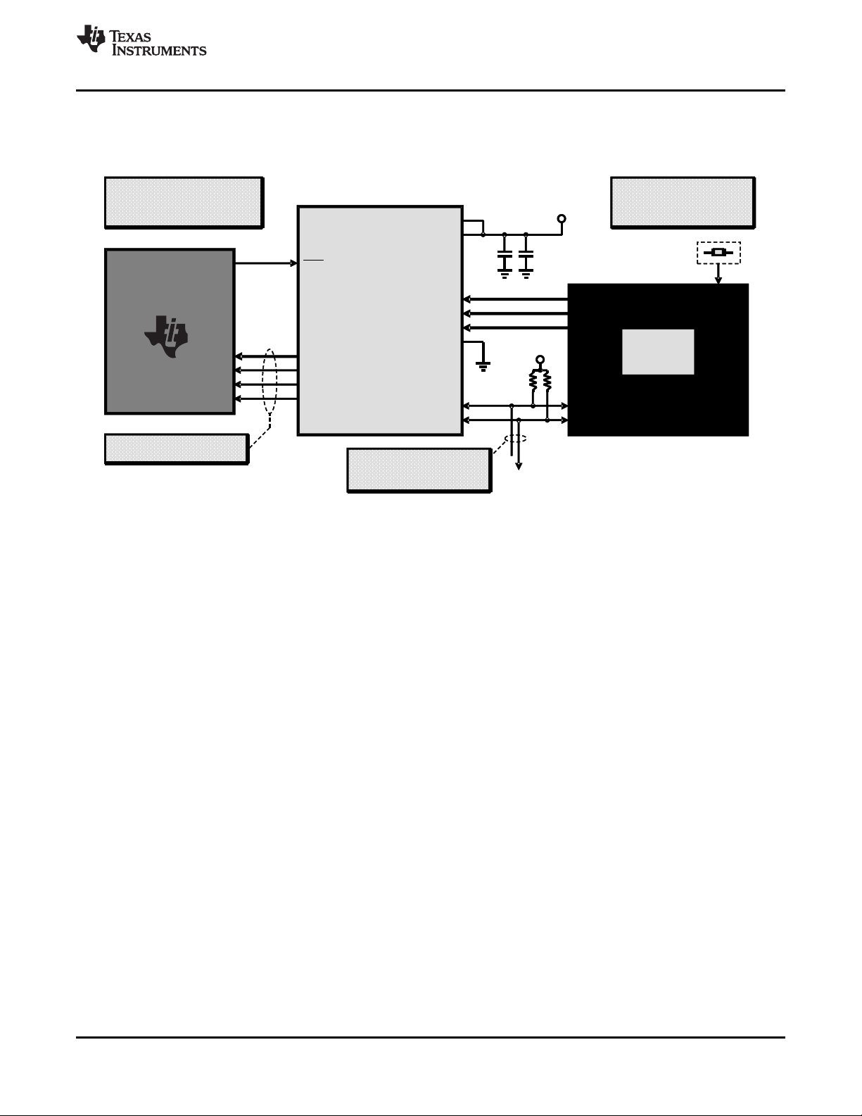
Aptina 1-Channel 2-Lane 12-bit Mode
Figure 20 illustrates the 720p60 1-Channel 2-Lane 12-bit per pixel operating mode.
SLLSED9 –NOVEMBER 2012
Decoupling Recommendations
To minimize the power supply noise floor, provide good decoupling near the SN65LVDS324 power pins. The use
of four ceramic capacitors (2x 0.01 µF and 2x 0.1 µF) provides good performance. At the very least, it is
recommended to install one 0.1 µF and one 0.01 µF capacitor near the SN65LVDS324. To avoid large current
loops and trace inductance, the trace length between decoupling capacitors and device power inputs pins must
be minimized. Placing the capacitor underneath the SN65LVDS324 on the bottom of the PCB is often a good
choice.
Copyright © 2012, Texas Instruments Incorporated Submit Documentation Feedback 19
Figure 20. 1-Channel 2-Lane 12bpp Application
Product Folder Links: SN65LVDS324
Page 20
PACKAGE OPTION ADDENDUM
www.ti.com
11-Apr-2013
PACKAGING INFORMATION
Orderable Device Status
SN65LVDS324ZQLR ACTIVE BGA
(1)
The marketing status values are defined as follows:
ACTIVE: Product device recommended for new designs.
LIFEBUY: TI has announced that the device will be discontinued, and a lifetime-buy period is in effect.
NRND: Not recommended for new designs. Device is in production to support existing customers, but TI does not recommend using this part in a new design.
PREVIEW: Device has been announced but is not in production. Samples may or may not be available.
OBSOLETE: TI has discontinued the production of the device.
Package Type Package
(1)
MICROSTAR
JUNIOR
Drawing
ZQL 59 1000 Green (RoHS
Pins Package
Qty
Eco Plan
(2)
& no Sb/Br)
Lead/Ball Finish MSL Peak Temp
(3)
Call TI Level-3-260C-168 HR -40 to 85 LVDS324
Op Temp (°C) Top-Side Markings
(4)
(2)
Eco Plan - The planned eco-friendly classification: Pb-Free (RoHS), Pb-Free (RoHS Exempt), or Green (RoHS & no Sb/Br) - please check http://www.ti.com/productcontent for the latest availability
information and additional product content details.
TBD: The Pb-Free/Green conversion plan has not been defined.
Pb-Free (RoHS): TI's terms "Lead-Free" or "Pb-Free" mean semiconductor products that are compatible with the current RoHS requirements for all 6 substances, including the requirement that
lead not exceed 0.1% by weight in homogeneous materials. Where designed to be soldered at high temperatures, TI Pb-Free products are suitable for use in specified lead-free processes.
Pb-Free (RoHS Exempt): This component has a RoHS exemption for either 1) lead-based flip-chip solder bumps used between the die and package, or 2) lead-based die adhesive used between
the die and leadframe. The component is otherwise considered Pb-Free (RoHS compatible) as defined above.
Green (RoHS & no Sb/Br): TI defines "Green" to mean Pb-Free (RoHS compatible), and free of Bromine (Br) and Antimony (Sb) based flame retardants (Br or Sb do not exceed 0.1% by weight
in homogeneous material)
(3)
MSL, Peak Temp. -- The Moisture Sensitivity Level rating according to the JEDEC industry standard classifications, and peak solder temperature.
(4)
Multiple Top-Side Markings will be inside parentheses. Only one Top-Side Marking contained in parentheses and separated by a "~" will appear on a device. If a line is indented then it is a
continuation of the previous line and the two combined represent the entire Top-Side Marking for that device.
Important Information and Disclaimer:The information provided on this page represents TI's knowledge and belief as of the date that it is provided. TI bases its knowledge and belief on information
provided by third parties, and makes no representation or warranty as to the accuracy of such information. Efforts are underway to better integrate information from third parties. TI has taken and
continues to take reasonable steps to provide representative and accurate information but may not have conducted destructive testing or chemical analysis on incoming materials and chemicals.
TI and TI suppliers consider certain information to be proprietary, and thus CAS numbers and other limited information may not be available for release.
In no event shall TI's liability arising out of such information exceed the total purchase price of the TI part(s) at issue in this document sold by TI to Customer on an annual basis.
Samples
Addendum-Page 1
Page 21
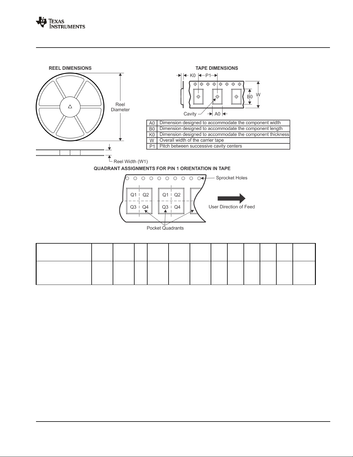
PACKAGE MATERIALS INFORMATION
www.ti.com 26-Jan-2013
TAPE AND REEL INFORMATION
*All dimensions are nominal
Device Package
SN65LVDS324ZQLR BGA MI
CROSTA
Type
R JUNI
OR
Package
Drawing
Pins SPQ Reel
Diameter
(mm)
ZQL 59 1000 330.0 16.4 4.8 7.3 1.5 8.0 16.0 Q1
Reel
Width
W1 (mm)
A0
(mm)B0(mm)K0(mm)P1(mm)W(mm)
Pin1
Quadrant
Pack Materials-Page 1
Page 22
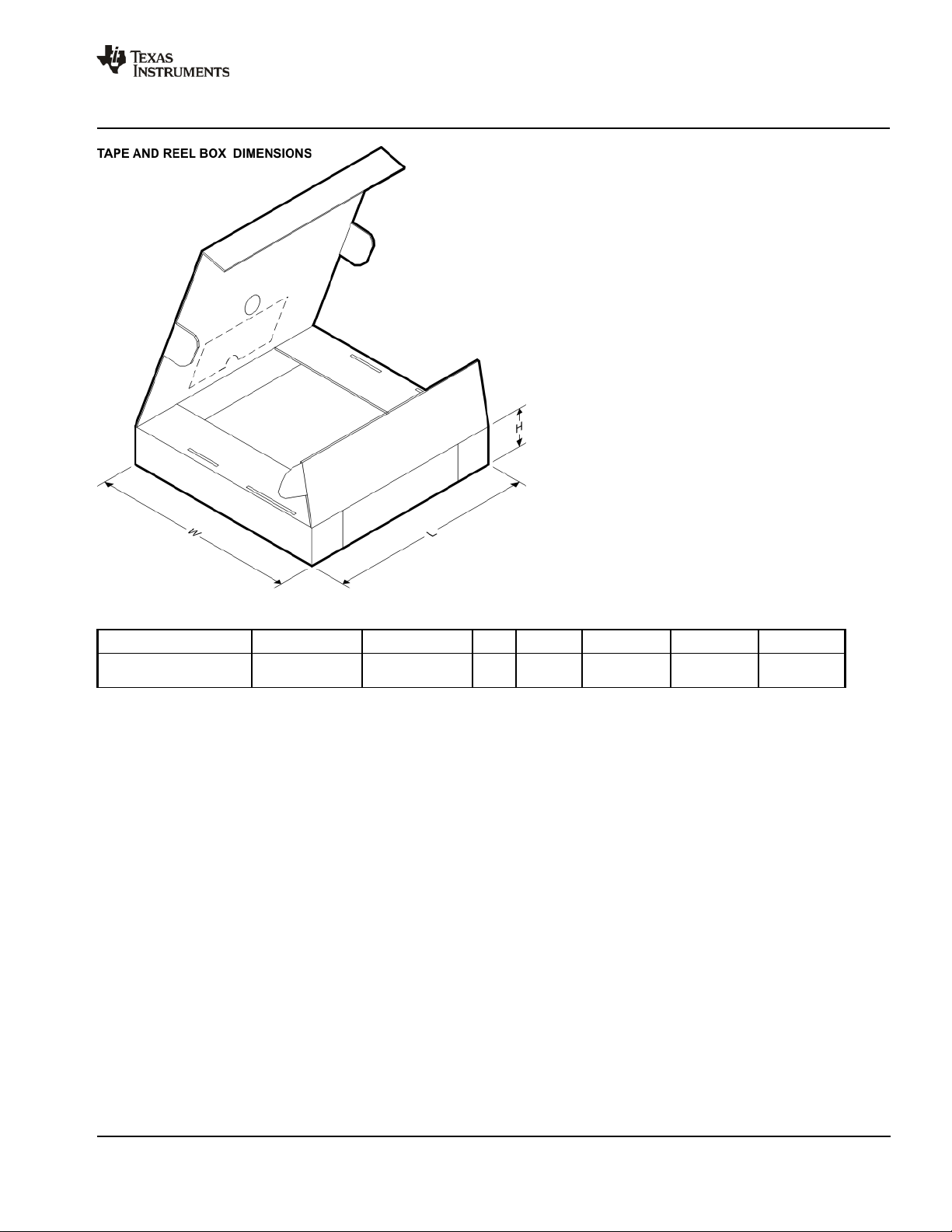
PACKAGE MATERIALS INFORMATION
www.ti.com 26-Jan-2013
*All dimensions are nominal
Device Package Type Package Drawing Pins SPQ Length (mm) Width (mm) Height (mm)
SN65LVDS324ZQLR BGA MICROSTAR
JUNIOR
ZQL 59 1000 336.6 336.6 31.8
Pack Materials-Page 2
Page 23
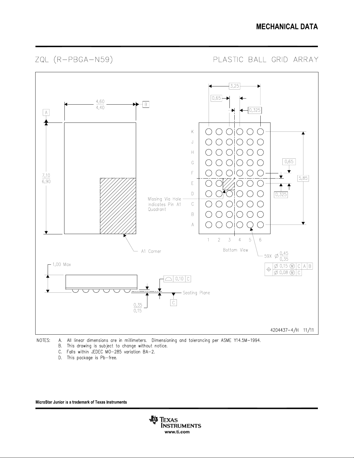
Page 24

IMPORTANT NOTICE
Texas Instruments Incorporated and its subsidiaries (TI) reserve the right to make corrections, enhancements, improvements and other
changes to its semiconductor products and services per JESD46, latest issue, and to discontinue any product or service per JESD48, latest
issue. Buyers should obtain the latest relevant information before placing orders and should verify that such information is current and
complete. All semiconductor products (also referred to herein as “components”) are sold subject to TI’s terms and conditions of sale
supplied at the time of order acknowledgment.
TI warrants performance of its components to the specifications applicable at the time of sale, in accordance with the warranty in TI’s terms
and conditions of sale of semiconductor products. Testing and other quality control techniques are used to the extent TI deems necessary
to support this warranty. Except where mandated by applicable law, testing of all parameters of each component is not necessarily
performed.
TI assumes no liability for applications assistance or the design of Buyers’ products. Buyers are responsible for their products and
applications using TI components. To minimize the risks associated with Buyers’ products and applications, Buyers should provide
adequate design and operating safeguards.
TI does not warrant or represent that any license, either express or implied, is granted under any patent right, copyright, mask work right, or
other intellectual property right relating to any combination, machine, or process in which TI components or services are used. Information
published by TI regarding third-party products or services does not constitute a license to use such products or services or a warranty or
endorsement thereof. Use of such information may require a license from a third party under the patents or other intellectual property of the
third party, or a license from TI under the patents or other intellectual property of TI.
Reproduction of significant portions of TI information in TI data books or data sheets is permissible only if reproduction is without alteration
and is accompanied by all associated warranties, conditions, limitations, and notices. TI is not responsible or liable for such altered
documentation. Information of third parties may be subject to additional restrictions.
Resale of TI components or services with statements different from or beyond the parameters stated by TI for that component or service
voids all express and any implied warranties for the associated TI component or service and is an unfair and deceptive business practice.
TI is not responsible or liable for any such statements.
Buyer acknowledges and agrees that it is solely responsible for compliance with all legal, regulatory and safety-related requirements
concerning its products, and any use of TI components in its applications, notwithstanding any applications-related information or support
that may be provided by TI. Buyer represents and agrees that it has all the necessary expertise to create and implement safeguards which
anticipate dangerous consequences of failures, monitor failures and their consequences, lessen the likelihood of failures that might cause
harm and take appropriate remedial actions. Buyer will fully indemnify TI and its representatives against any damages arising out of the use
of any TI components in safety-critical applications.
In some cases, TI components may be promoted specifically to facilitate safety-related applications. With such components, TI’s goal is to
help enable customers to design and create their own end-product solutions that meet applicable functional safety standards and
requirements. Nonetheless, such components are subject to these terms.
No TI components are authorized for use in FDA Class III (or similar life-critical medical equipment) unless authorized officers of the parties
have executed a special agreement specifically governing such use.
Only those TI components which TI has specifically designated as military grade or “enhanced plastic” are designed and intended for use in
military/aerospace applications or environments. Buyer acknowledges and agrees that any military or aerospace use of TI components
which have not been so designated is solely at the Buyer's risk, and that Buyer is solely responsible for compliance with all legal and
regulatory requirements in connection with such use.
TI has specifically designated certain components as meeting ISO/TS16949 requirements, mainly for automotive use. In any case of use of
non-designated products, TI will not be responsible for any failure to meet ISO/TS16949.
Products Applications
Audio www.ti.com/audio Automotive and Transportation www.ti.com/automotive
Amplifiers amplifier.ti.com Communications and Telecom www.ti.com/communications
Data Converters dataconverter.ti.com Computers and Peripherals www.ti.com/computers
DLP® Products www.dlp.com Consumer Electronics www.ti.com/consumer-apps
DSP dsp.ti.com Energy and Lighting www.ti.com/energy
Clocks and Timers www.ti.com/clocks Industrial www.ti.com/industrial
Interface interface.ti.com Medical www.ti.com/medical
Logic logic.ti.com Security www.ti.com/security
Power Mgmt power.ti.com Space, Avionics and Defense www.ti.com/space-avionics-defense
Microcontrollers microcontroller.ti.com Video and Imaging www.ti.com/video
RFID www.ti-rfid.com
OMAP Applications Processors www.ti.com/omap TI E2E Community e2e.ti.com
Wireless Connectivity www.ti.com/wirelessconnectivity
Mailing Address: Texas Instruments, Post Office Box 655303, Dallas, Texas 75265
Copyright © 2013, Texas Instruments Incorporated
 Loading...