

Datasheet ILC7070HCM-30, ILC7070HCM-25, ILC7070HCM-50, ILC7070HCM-33 Datasheet (Impala Linear Corporation)
Page 1
150mA CMOS LDO regulator in a 5-lead SOT-23 package,
featuring 120mV dropout at 100mA levels and nearly negligible dropout below 5mA.
The part offers ±2% precision as standard, yet draws only
5µA of current in operation and drops to 0.5µA in shutdown.
The outputs offer short-circuit protection, and the shutdown
pin has an internal pull-down which will disable the output if
the pin is left floating.
ILC7070
SOT-23 CMOS LDO Regulator with Shutdown
Impala Linear Cor poration
Impala Linear Corporation
1
(408) 574-3939
www.impalalinear.com
Oct 1999
ILC7070 1.1
• All-CMOS design in 5-lead SOT-23 package
• ±2% precision outputs
• Up to 150mA output current
• 120mV dropout at 100mA load
• Only 5µA quiescent current at full load
• 0.5µA quiescent current in shutdown
• Voltage options allow:
50mA 5V Regulator
50mA 5V to 3.3, 3.0, or 2.5V Convertor
150mA 3.3V or 3.0V to 2.5V Convertor
• Battery-powered Equipment
• Reference voltage sources
• Portable Cameras and Video Recorders
• PDAs
ILC7070HCM-25
50mA 5V to 2.5V regulator, or 150mA 3.x to 2.5V regulator, High-level true Chip Enable
ILC7070HCM-30
50mA 5V to 3.0V regulator, High-level true Chip Enable
ILC7070HCM-33
50mA 5V to 3.3V regulator, High-level true Chip Enable
ICL7070HCM-50
30mA 5V regulator, High-level true Chip Enable
31
2
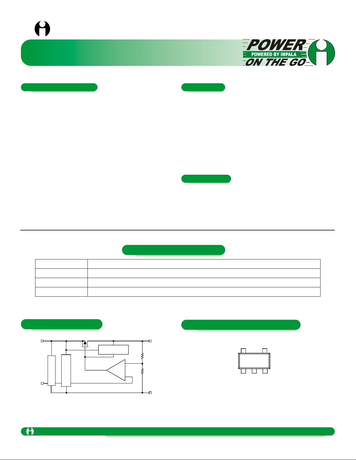
SOT-23-5
(TOP VIEW)
(NC) VINCE
4
5
V
OUT
V
SS
-
+
SHORT-CIRCUIT
PROTECT
V
SS
V
OUT
V
IN
REFERENCE VOLTAGE
SOURCE
SHUTDOWN CONTROL
CE
General Description
Features
Applications
Ordering Information
Block Diagram
Pin-Package Configurations
Page 2
SOT-23 CMOS LDO Regulator with Shutdown
Impala Linear Corporation
2
(408) 574-3939
www.impalalinear.com
Oct 1999
ILC7070 1.1
Parameter
Symbol
Ratings
Units
Input Voltage
V
IN
12
V
CE Input Voltage
V
CE
VSS-.0.3~VIN + 0.3
V
Output Current
I
OUT
500
mA
Output Voltage
V
OUT
VSS-0.3~VIN + 0.3
V
Continuous Total
Power Dissipation
P
d(max)
150
mW
Operating Ambient
Temperature
T
opr
-30~+80
°C
Storage Temperature
T
stg
-40~+125
°C
Parameter
Symbol
Conditions
Min
Typ
Max
Units
Output Voltage
V
OUT
I
OUT
= 40mA, VIN = 6.0V
4.90
5.0
5.10
V
Maximum Output Current
I
OUT
max
VIN = 6.0V, V
OUT
> 4.5V
125
mA
Load Stability
∆V
OUT
VIN = 6.0V, 1mA < I
OUT
< 100mA
80
mV
Input/Output
Voltage Differential
V
dif
I
OUT
= 100mA, V
OUT
= V
SET
x 0.98
200
300
mV
Supply Current 1
ISS1
VIN = V
CE
= 6.0V
6 12
µA
Supply Current 2
ISS2
VIN = 6.0V, VCE = open (Note 5)
0.5
2.0
µA
Input Stability
∆V
OUT
∆VIN • V
OUT
I
OUT
= 40mA
6.0V < VIN < 10.0V
0.3
%/V
Input Voltage
V
IN
10
V
Output Voltage
Temperature Characteristics
∆V
OUT
∆T
opr
• V
OUT
I
OUT
= 40mA
-30°C < T
opr
< 80°C
±100
ppm/
°C
CE Input Current
I
IH
I
IL
VIN = 6.0V, VCE = 2.5V
VIN = 6.0V, VCE = 0
2 4
0.1
µA
CE ON Voltage
CE
(ON)
VIN = 6.0V
2.5 V
IN
V
CE OFF Voltage
CI
(OFF)
VIN = 6.0V
0 0.7
V
Note: I
OUT
must be less than P
d(max)
/ (VIN-V
OUT
)
Absolute Maximum Ratings (TA= 25°C)
Electrical Characteristics ILC7070HCM-50
V
OUT
= 5.0V, TA=25°C
Page 3

SOT-23 CMOS LDO Regulator with Shutdown
Impala Linear Corporation
3
(408) 574-3939
www.impalalinear.com
Oct 1999
ILC7070 1.1
Parameter
Symbol
Conditions
Min
Typ
Max
Units
Output Voltage
V
OUT
I
OUT
= 40mA, VIN = 3.5V
2.450
2.5
2.55
V
Maximum Output Current
I
OUT
max
VIN = 3.5V, V
OUT
> 2.25V
125
mA
Load Stability
∆V
OUT
VIN = 3.5V, 1mA < I
OUT
< 60mA
45
90
mV
Input/Output
Voltage Differential
V
dif
I
OUT
= 60mA, V
OUT
= V
SET
x .98
180
360 mV
Supply Current 1
ISS1
VIN = VCE = 3.5V
5 10
µA
Supply Current 2
ISS2
VIN = 3.5V, VCE = open (Note 5)
0.5 2 µA
Input Stability
∆V
OUT
∆VIN • V
OUT
I
OUT
= 40mA
3.5V<
VIN < 10V
0.2
0.3
%/V
Input Voltage
V
IN
10.0
V
Output Voltage
Temperature Characteristics
∆V
OUT
∆T
opr
• V
OUT
I
OUT
= 40mA
-30°C <
T
opr
< 80°C
±100
ppm/°C
CE Input Current
I
IH
I
IL
VIN = 3.5V, VCE = 3.5V
V
IN
= 3.5V, VCE = 0V
2 4
0.1
µA
CE ON Voltage
CE
(ON)
VIN = 3.5V
2.5 VIN
V
CE OFF Voltage
CE
(OFF)
VIN = 3.5V
0 0.7
V
Note:
1. V
OUT
means the output voltage when “V
OUT
+ 1.0V” is provided at the VINpin while maintaining a certain I
OUT
value.
2. V
IN
1 is defined as the input value that is gradually decreased until the output value reaches V
OUT
x 98%.
3. V
dif
is defined as “VIN1-V
OUT.
”
4. I
OUT
: this is limited by continuous total power dissipation in the package.
5. When V
CE
is LOW or OPEN, the output is disabled.
Note: CE pin is a CMOS input. Because of this, when the input voltage reaches V
IN
/2, a rush current will start to flow.
Electrical Characteristics ILC7070HCM-25
V
OUT
= 2.5V, TA= 25°C
Page 4

SOT-23 CMOS LDO Regulator with Shutdown
Impala Linear Corporation
4
(408) 574-3939
www.impalalinear.com
Oct 1999
ILC7070 1.1
OUTPUT VOLTAGE vs OUTPUT CURRENT
OUTPUT VOLTAGE vs INPUT VOLTAGE
OUTPUT VOLTAGE vs INPUT VOLTAGE
V
DO
vs OUTPUT CURRENT
OUTPUT VOLTAGE vs INPUT VOLTAGE
OUTPUT VOLTAGE vs INPUT VOLTAGE
ILC7070HCM-50
ILC7070HCM-50
ILC7070HCM-50
ILC7070HCM-30
ILC7070HCM-30
OUTPUT VOLTAGE V
OUT
(V)
3.1
3.0
2.9
2.8
0 20 40 60 80 100 120 140 160
OUTPUT CURRENT I
OUT
(mA)
VIN= 4.0V
VIN= 6.0V
T
opr
= -30°C
T
opr
= 25°C
T
opr
= 25°C
T
opr
= 25°C
T
opr
= 25°C
I
OUT
= 1mA
I
OUT
= 1mA
I
OUT
= 1mA
I
OUT
= 1mA
T
opr
= -30°C
25°C
25°C
40mA
40mA
10mA
10mA
80°C
80°C
OUTPUT VOLTAGE V
OUT
(V)
5.1
5.0
4.9
4.8
0 40 80 120 160 200
OUTPUT CURRENT I
OUT
(mA)
4.5 5.0 5.5
INPUT VOLTAGE VIN(V)
5.1
5.0
4.8
4.6
4.4
4.2
OUTPUT VOLTAGE V
OUT
(V)
OUTPUT VOLTAGE V
OUT
(V)
3.2
3.0
2.8
2.6
2.4
2.2
2.5 3.0 3.5
INPUT VOLTAGE VIN(V)
3.0 4.0 5.0 6.0 7.0 8.0 9.0 10
V
DO
(V)
V
DO
(V)
OUTPUT VOLTAGE V
OUT
(V)
INPUT VOLTAGE VIN(V)
5.05
5.04
5.03
5.02
5.01
5.00
4.99
4.98
5.0 6.0 7.0 8.0 9.0 10
INPUT VOLTAGE VIN(V)
ILC7070HCM-30
1.0
0.8
0.6
0.4
0.2
0.0
-0.2
-0.4
0 40 80 120 160 200
OUTPUT CURRENT I
OUT
(mA)
80°C
80°C
-30°C
-30°C
T
opr
= 25°C
T
opr
= 25°C
0 20 40 60 80 100 120 140 160
0.6
0.5
0.4
0.3
0.2
0.0
-0.2
OUTPUT CURRENT I
OUT
(mA)
OUTPUT VOLTAGE vs OUTPUT CURRENT
ILC7070HCM-30
OUTPUT VOLTAGE V
OUT
(V)
3.04
3.03
3.02
3.01
3.00
2.99
2.98
2.97
V
DO
vs OUTPUT CURRENT
ILC7070HCM-50
Typical Performance Characteristics General conditions for all curves
Page 5

SOT-23 CMOS LDO Regulator with Shutdown
Impala Linear Corporation
5
(408) 574-3939
www.impalalinear.com
Oct 1999
ILC7070 1.1
OUTPUT VOLTAGE vs TEMPERATURE
OUTPUT VOLTAGE vs TEMPERATURE
LINE TRANSIENT RESPONSE
LINE TRANSIENT RESPONSE
ILC7070HCM-30
ILC7070HCM-50
ILC7070HCM-50
ILC7070HCM-50
VIN= 4.0V
VIN= 6.0V
I
OUT
= 10mA
I
OUT
= 10mA
I
OUT
= 10mA
I
OUT
= 1mA
Input Voltage
Input Voltage
Output Voltage
Output Voltage
40mA
40mA
-40 -20 0 20 40 60 80 100
-40 -20 0 20 40 60 80 100
T
opr
(°C)
-1 0 1 2 3
TIME (ms)
TIME (ms)
(V)
(V)
8.0
7.5
7.0
6.5
6.0
5.5
5.0
4.5
4.0
8.0
7.5
7.0
6.5
6.0
5.5
5.0
4.5
4.0
-1 0 1 2 3
OUTPUT VOLTAGE V
OUT
(V)
3.01
3.00
2.99
2.98
2.97
2.96
2.95
2.94
OUTPUT VOLTAGE V
OUT
(V)
5.02
5.01
5.00
4.99
4.98
4.97
4.96
4.95
T
opr
(°C)
Electrical Characteristics General conditions for all curves
Page 6

SOT-23 CMOS LDO Regulator with Shutdown
Impala Linear Corporation
6
(408) 574-3939
www.impalalinear.com
Oct 1999
ILC7070 1.1
Package Outline Dimensions
0.118 (3.00)
0.102 (2.60)
0.037 (0.95) BSC
PIN 1
0.071 (1.80)
0.055 (1.40)
0.0059 (0.15)
0.0019 (0.05)
0.019 (0.50)
0.0138 (0.35)
0.057 (1.45)
0.035 (0.90)
SEATING
PLANE
10°
0°
0.0078 (0.2)
0.0031 (0.08)
0.0217 (0.55)
0.0138 (0.35)
0.055 (1.40)
0.0393 (1.0)
0.122 (3.10)
0.106 (2.70)
Devices sold by Impala Linear Corporation are covered by the warranty and patent indemnification provisions appearing in
its Terms of Sale only. Impala Linear Corporation makes no warranty, express, statutory, implied, or by description regarding the information set forth herein or regarding the freedom of the described devices from patent infringement. Impala
Linear Corporation makes no warranty of merchantability or fitness for any purpose. Impala Linear Corporation reserves
the right to discontinue production and change specifications and prices at any time and without notice.
This product is intended for use in normal commercial applications. Applications requiring an extended temperature
range, unusual environmental requirements, or high reliability applications, such as military and aerospace, are specifically not recommended without additional processing by Impala Linear Corporation.
Impala Linear Corporation assumes no responsibility for the use of any circuitry other than circuitry embodied in an
Impala Linear Corporation product. No other circuits, patents, licenses are implied.
Life Support Policy
Impala Linear Corporation’s products are not authorized for use as critical components in life support devices or systems.
1. Life support devices or systems are devices or systems which, (a) are intended for surgical implant into the body, or (b)
support or sustain life, and whose failure to perform, when properly used in accordance with instructions for use provided in
the labeling, can be reasonably expected to result in a significant injury to the user.
2. A critical component is any component of a life support dice or system whose failure to perform can be reasonably expected to cause the failure of the life support device or system, or to affect its safety or effectiveness.
 Loading...