

Page 1
Impala Linear Corporation
1
(408) 574-3939
www.impalalinear.com
June 1999
ILC6377 1.3
The ILC6377 is a 95% efficient, 300kHz step-down DC-DC
converter in an SO-8 package; capable of delivering 500mA
output current. The device is also capable of driving an
external FET for higher output current applications.
The ILC6377 uses a unique p-channel architecture with
built-in charge pump to maintain low on-resistance, even at
low input voltages. At high or normal currents the ILC6377
operates in PWM mode with 300kHz operating frequency.
When the load current drops and the device hits approximately 17% duty cycle, it automatically switches over to
PFM or pulse skipping mode. PFM (pulse frequency modulation) mode of operation extends efficiency at light loads.
Start-up is controlled via an external soft-start capacitor. The
device will automatically re-enter start-up mode when an
output current overload condition is sensed; thus providing
automatic short-circuit protection. Voltage lockout prevents
faulty operation below the minimum operating voltage level.
In shutdown, the ILC6377 consumes only 1.5mA current.
The ILC6377SO-XX offers fixed 3.3V or 5V ouput while
ILC6377SO-Adj allows adjustable output. Both versions of
ILC6377 are available in an SO-8 surface mount package.
! ±2.5% accurate output voltages
! Guaranteed 500mA output current
! 95% efficiency
! 55mA no load battery input current
! 1.5mA shutdown current
! Built in short circuit and overcurrent protection
! Undervoltage lockout and soft-start
! External transistor drive available for higher Iout
! 300kHz operation
! Automatic switchover to PFM mode at low
currents for longest battery life
! Fixed 3.3V or 5V or adjustable output
! SO-8 package
! Cellular Phones
! Palmtops and PDAs
! Portable Instrumentation
! Buck Converter for Industrial / Networking Applications
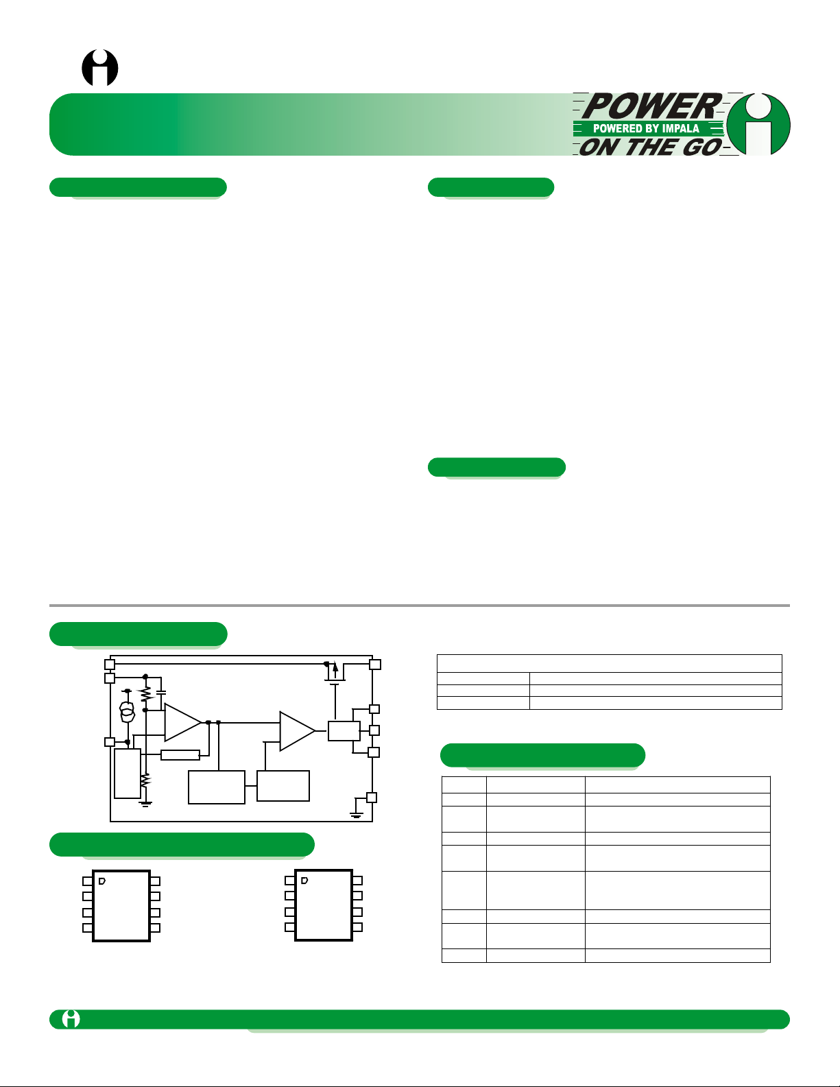
PWM/PFM
Protection
L
X
GND
EXT1
RA MP WAVE
V
IN
V
OUT
P_BST
GA TE
DR IV ER
GENERATOR,
OSCILLATORCONTROLLER
+
-
PWM
Comp
EXT2
+
-
Error
Amp
1
5
4
6
3
2
7
8
S/D,
Softstart,
Vref
S/D,
Vref
with
Soft-
start
ILC6377
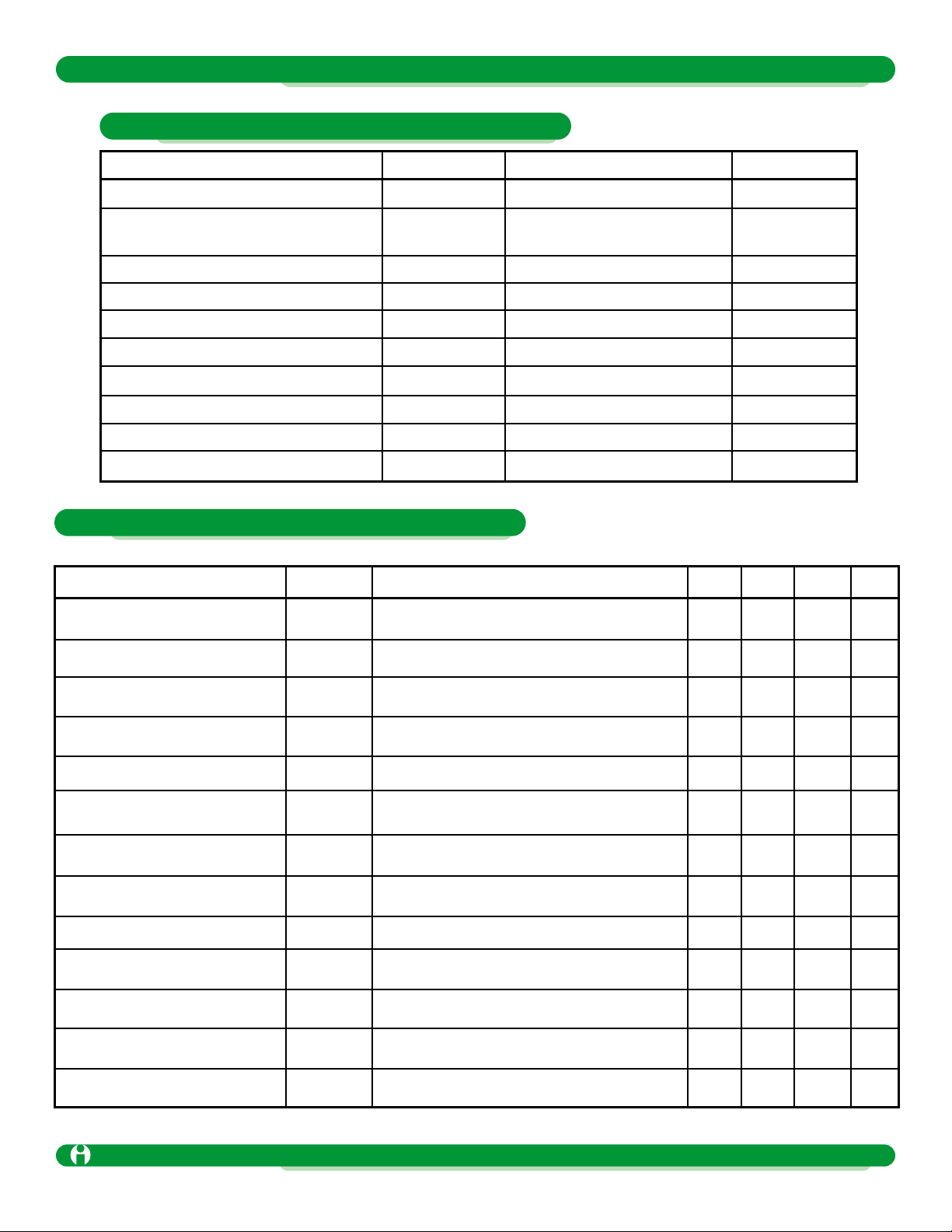
(TOP VIEW)
3
45
1
2
6
7
8 L
X
FB
EXT1
S/D,
GND
P_BST
EXT2
V
IN
ILC6377SO-Adj
C
SS
SO-8 Package
ILC6377
(TOP VIEW)
3
L
X
V
OUT
EXT1
45S/D,
GND
1
2
6
7
8
P_BST
EXT2
V
IN
C
SS
SO-8 Package
ILC6377SO-XX
Ordering Information
ILC6377SO-33 3.3V, 300 kHz step-down PWM/PFM converter
ILC6377SO-50 5V, 300 kHz step-down PWM/PFM converter
ILC6377SO-Adj Adjustable, 300 kHz step-down PWM/PFM converter
Pin
Symbol
Function
1
VIN
Power Supply
2
EXT2
External gate drive pin (low when
P-Ch FET is ON)
3
P-BST
P-Ch gate boost
4
S/D
Softstart, V
ref
Shutdown, also soft-start capacitor
pin and V
ref
output
5
V
OUT
/FB
Output voltage sense pin for
ILC6377SO-XX; 1V feedback for
ILC6377SO adj
6
GND
Ground connection
7
EXT1
External gate drive pin (low when
P-Ch FET is on)
8
LX
Inductor switch pin
ILC6377
0.5A, 300kHz, SO-8 PWM/PFM Step Down
Converter with Shutdown
Impala Linear Cor poration
General Description
Features
Applications
Block Diagram
Pin Package Configurations
Pin Description
Page 2
0.5A, 300kHz, SO-8 PWM/PFM Step Down Converter with Shutdown
Impala Linear Corporation
2
(408) 574-3939
www.impalalinear.com
June 1999
ILC6377 1.3
Conditions
V
IN
3.5V, No Loads
V
S/D
= 0V
Open Loop Measurement, V
S/D
= VIN, V
LX
=
VIN- 0.4V , V
OUT
= 3V
Open Loop Measurement, V
OUT
= VIN,
V
LX
= 0V
Measurement Waveform at EXT pin VIN=
3.6V I
OUT
= 20mA
No Load
Minimum V
IN
when V
ref
does not start up
V
ref
rises to 0V from 0.9V
Parameter
Output Voltage
Input Voltage
Output Voltage
Input Current Supply
Shutdown Current
LX Switch On - Resistance
LXSwitch Leakage Current
Oscillator Frequency
Max Duty Cycle
PFM Duty Cycle
Efficiency
Undervoltage Lockout
Soft-Start Time
Symbol
V
OUT
V
IN
I
OUT
I
IN
I
S/D
R
ds(on)
I
LXL
F
OSC
MAXDTY
PFMDTY
EFFI
V
UVLO
T
SS
Unless Otherwise specified all limits are at V
OUT
= 3.3V, VIN= 4V, F
OSC
=300kHz, I
OUT
= 130mA,TA= 25°C. Circuit configuration of figure 1.
Parameter
V
IN
Input Voltage Pin
V
OUT
Pin (ILC6370SO-XX)
FB Pin (ILC6377SO-Adj)
Voltage on LXpin
Peak Switch Current on LXpin
Voltage on P_BST pin
Current EXT1, EXT2 pins
Voltage on all other pins
Continuous Total Power Dissipation
Operating Ambient Temperature
Storage Temperature
Symbol
V
IN
V
OUT
V
FB
V
LX
I
LX
VDP_BST
I
EXT1, IEXT2
~
P
D
T
OPR
T
STG
Ratings
-0.3 to +12
-0.3 to +12
-0.3 to VIN+12
VIN- V
LX
= 0.3 to +12
700
VIN- VP_BST = 0.3 to +12
±50
-0.3 to V
IN
500
-30~+80
-40~+125
Units
V
V
V
mA
V
mA
V
mA
°C
°C
Typ
3.300
600
55
1.5
0.64
300
100
17
95
10.0
Min
3.218
500
255
10
1
6.0
Max
3.383
10
86
2.5
0.85
2.0
345
25
1.8
16.0
Units
V
V
mA
µA
µA
Ω
µA
kHz
%
%
%
V
msec
Absolute Maximum Ratings (TA=25°C)
Electrical Characteristics ILC6377SO-33
Page 3
0.5A, 300kHz, SO-8 PWM/PFM Step Down Converter with Shutdown
Impala Linear Corporation
3
(408) 574-3939
www.impalalinear.com
June 1999
ILC6377 1.3
Min
4.875
500
255
10
1
6.0
3.0
0.65
Typ
5.000
600
71
1.5
0.44
300
100
17
95
10.0
5.0
24
20
Symbol
V
OUT
V
IN
I
OUT
I
IN
I
S/D
R
ds(on)
I
LXL
F
OSC
MAXDTY
PFMDTY
EFFI
V
UVLO
T
SS
T
PRO
V
S/D
REXt
HI
REXt
LOW
Parameter
Output Voltage
Input Voltage
Output Current
Input Supply Current
Shutdown Current
LXSwitch On-Resistance
LXSwitch Leakage Current
Oscillator Frequency
Max Duty Cycle
PFM Duty Cycle
Efficiency
Undervoltage Lockout
Soft-Start Time
Internal Protection Time
Shutdown Input Voltage
EXT1, EXT2 Hi On-Resistance
EXT1, EXT2 Low On-Resistance
Parameter
Internal Protection Time
Shutdown Input Voltage
EXT1, EXT2 Hi On-Resistance
EXT1, EXT2 Low On-Resistance
Symbol
T
PRO
V
SD
REXt
HI
REXt
LOW
Conditions
Time from V
OUT
= 0V to V
S/D
going low
High = Regulator “ON”
Low = Regulator “OFF”
3V applied to V
OUT
with no external components
3.6V applied to V
OUT
with no external components
Min
3.0
0.65
Typ
5.0
3.5
29
Max
8.0
0.2
47
37
Units
Msec
V
Ω
Ω
Conditions
V
IN
5.25V, No Load
V
S/D
= 0V
Open Loop Measurement, V
S/D
= VIN,
V
LX =VIN
- 0.4V, V
OUT
= 4.5V
Open Loop Measurement, V
OUT
= VIN,
VLX= 0V
Measure Waveform at EXT pin V
IN
= 5.3V
I
OUT
= 20mA
No Load
Minimum VINwhen V
ref
does not start up
V
ref
rises to 0V from 0.9V
Time form V
OUT
m = 0V to V
S/D
going low
High = Regulator “ON”
Low = Regulator “OFF”
Open Loop Measurement
Open Loop Measurement
Max
5.125
10
110
2.5
0.58
2.0
345
25
1.8
16.0
8.0
0.2
32
26
Units
V
V
mA
µA
µA
Ω
µA
kHz
%
%
%
V
msec
msec
V
Ω
Ω
Electrical Characteristics ILC6377SO-33
Electrical Characteristics ILC6377SO-50
Unless Otherwise specified all limits are at V
OUT
= 3.3V, VIN= 4V, F
OSC
=300kHz, I
OUT
= 130mA,TA= 25°C. Circuit configuration of figure 1.
Unless Otherwise specified all limits are at V
OUT
= 5.0V, VIN= 6V, F
OSC
=300kHz, I
OUT
= 200mA, TA= 25°C. Circuit configuration of figure 1.
Page 4
0.5A, 300kHz, SO-8 PWM/PFM Step Down Converter with Shutdown
Impala Linear Corporation
4
(408) 574-3939
www.impalalinear.com
June 1999
ILC6377 1.3
Parameter Symbol Conditions Min Typ Max Units
Feedback Voltage (pin5) V
FB
.995 1.000 1.015 V
Input Voltage V
OUT
R
FB1
+ R
FB2
< 2MΩ 38V
Output Current I
OUT
500 600 mA
Input Supply Current I
IN
VIN5.25V, No Load 71 110 µA
Shutdown Current I
S/D
V
S/D
= 0V 1.5 2.5 µA
LX Switch On-Resistance R
ds(on)
Open Loop Measurement, V
S/D
= VIN, 0.44 0.58 Ω
V
LX
= VIN- 0.4V, V
OUT
= 4.5V
LX Switch On-Resistance I
LXL
Open Loop Measurement, V
OUT
= VIN, 2.0 µA
V
LX
= 0V
Shutdown Input Voltage V
S/D
High = Regulator “ON” 0.65 0.2 V
Low = Regulator “OFF”
Oscillator Frequency F
OSC
Measure Waveform at EXT pin VIN= 255 300 345 kHz
5.3V I
OUT
= 20mA
Max Duty Cycle MAXDTY 100 %
PFM Duty Cycle PFMDTY No Load 10 17 25 %
Efficiency EFFI 95 %
Undervoltage Lockout V
UVLO
Minimum VINwhen V
ref
does not start up 1 1.8 V
Soft-Start Time T
SS
V
ref
rises to 0V from 0.9V 6.0 10.0 16.0 msec
Internal Protection Time T
PRO
Time from V
OUT
m = 0V to V
S/D
going low 3.0 5.0 8.0 msec
EXT1, EXT2 Hi On-Resistance REXt
HI
Open Loop Measurement 24 32 Ω
EXT1, EXT2 Low On-Resistance REXt
LOW
Open Loop Measurement 20 26 Ω
Electrical Characteristics ILC6377SO-Adj
Unless Otherwise specified all limits are at V
OUT
programmed to 5.0V, VIN= 6V, F
OSC
=300kHz, I
OUT
= 200mA, TA= 25°C. Circuit configuration of figure 1.
Page 5

0.5A, 300kHz, SO-8 PWM/PFM Step Down Converter with Shutdown
Impala Linear Corporation
5
(408) 574-3939
www.impalalinear.com
June 1999
ILC6377 1.3
+
V
OUT
ILC6377
(TOP VIEW)
3
45
1
2
6
7
8
+
CL
V
IN
S/D
C
SS
SD1
L
*C
IN
Fig 1 . Typi cal ste p-down DC-DC
c onver ter applic at io n
SD1 : MA735 Schottky Diode ( MATSUSHITA )
C
L
: 10 V /4 7 µF Tantalum Capacitor ( NICHICON, F93 )
C
SS
: 4700pF Ceramic Capacitor
C
IN
: 16V / 10µF Tantalum Capacitor ( NICHICON, F93 )
22µH
47µF
10µF
External component selection
Proper selection of external components is important for
achieving high performance. The output inductor selected
should have low DC resistance on the order of 0.2W or less
and saturation current rating of 1A or higher.
Recommended inductors are Sumida CD54 (22mH, 0.18W
max DC resistance) or Coilcraft DO3308P-223 (22mH,
0.18W max DC resistance) or equivalent.
The catch diode should be a schottky diode with low for-
ward drop and rated at 1A or greater current, MA735 or it’s
equivalent is recommended.
Input and output capacitors should be tantalum capacitors
with low equivalent series resistance (ESR) and voltage rating higher than the actual application.
Soft-start
Pin 4 of ILC6377 functions as the soft-start pin as well as the
shutdown pin. A soft-start capacitor (from pin 4 to ground)
controls the rate at which the power supply starts up; thus
preventing large overshoots at the output as well as large inrush current. The value for CSS should be 100pF or greater.
Shutdown
The ILC6377 is placed in shutdown mode by taking pin 4 to
ground. In shutdown, the quiescent current of the device is
under 2mA. When using the shutdown feature, pin 4 must
be driven from an open collector or open drain output without employing an external pull-up resistor, as shown in figure 2. Since pin 4 is also used to charge an external capacitor for soft-start, this pin should not be driven from a pushpull CMOS type output.
Over-current and short-circuit protection
In the event of an over-current or short-circuit condition, the
ILC6377 cycles the soft-start pin in a hiccup mode to provide
fault protection. When the output voltage decreases due to
overload, the ILC6377 will operate continuously at the maximum duty cycle. If the period of maximum duty cycle operation exceeds TPRO (typically 5 msec), pin 4 will be pulled
low; thus discharging the external soft-start capacitor CSS.
This action inhibits the regulator’s PWM action. Next, the
ILC6377’s soft-start circuitry starts recharging CSS and initiates a controlled start-up. If the overload condition continues
to exist, the above sequence of events will repeat; thus continuing to cycle the soft-start function.
Note that very little power is dissipated with this method of
fault protection versus constant current limit protection.
Even though the internal power MOSFET is pulsed on and
off at high peak current, the DC current is low; thus leading
to low power dissipation even under short-circuit conditions.
Keep in mind that the duration of maximum duty cycle
condition is used to trigger the
ILC6377’s fault protec-
tion circuit. As such, a small input-output (V
IN
- V
OUT
)
differential voltage may trigger the device’s fault protection circuitry even at low output current.
Undervoltage Lockout
The undervoltage lockout feature prevents faulty operation
by disabling the operation of the regulator when input volt-
age is below the minimum operating voltage, VUVLO. When
the input voltage is lower than VUVLO the device disables
the internal P-channel MOSFET and provides “high” output
at both EXT1 and EXT2 outputs.
Figure 2 shows a typical fixed output voltage step-down DC-DC
converter application circuit for ILC6377SO-XX
Fig. 1: Typical step-down wn DC-DC
converter application
Page 6

0.5A, 300kHz, SO-8 PWM/PFM Step Down Converter with Shutdown
Impala Linear Corporation
6
(408) 574-3939
www.impalalinear.com
June 1999
ILC6377 1.3
The EXT1 and EXT2 pins are provided so as to drive
external transistors; thus allowing design flexibility.
The EXT output drive signal has the same timing as
the gate drive to the internal P-channel MOSFET i.e.
EXT output is low as long as the internal MOSFET is
on. Both EXT1 and EXT2 pins are capable of driving
1000pF gate capacitance. For example, a high output current application circuit using an external Pchannel MOSFET is shown in figure 2.
V
OUT
ILC6377
(TOP VIEW)
3
45
1
2
6
7
8
+
CL
+
V
IN
S/D
C
SS
SD1
L
*C
IN
EXT1
Fig.2 1Am p output c ur r ent appli ca tion
usi ng ex te rn al MOSFET
Figure 3. P-Channel Negative
C
BST
Voltage between Vin and
ILC6377
(TOP VI EW )
3
4
5
1
2
6
7
8
SD1
2200pF
MA729
Schottky
P-Channel Boost Circuit
The ILC6377 includes a unique P-Channel MOSFET
architecture with built-in charge pump to maintain low
on-resistance even at low input voltages. As shown in
figure 3, a 2200pF ceramic capacitor and a schottky
diode ( MA729 or equivalent ) allows the gate voltage
of the internal P-Channel MOSFET to be driven negative; thus reducing the switch on-resistance. This
technique can be employed to increase efficiency at
low input voltages and high output currents.
Note that the voltage between V
IN
and P_BST should not
exceed 10V, otherwise damage to the device may occur.
For high input voltage applications the schottky diode
should be replaced by a low voltage zener diode so that the
P_BST pin is clamped to a safe negative voltage.
V
OUT
5
6
C
FB
R
FB1
R
FB2
R
FB1
+ R
FB2
≤ 2MΩ
C
FB
chosen so that 1kHz
1
2 π× CF B× RFB1×
-----------------------------------------------------
20kHz<<
T o pin 8
Fig.4 Adjustable output using I LC6377SO-Adj
( Note : rest of circuit is same as Fig.1 )
Adjustable Output ( ILC6377SO-Adj )
For adjustable output voltage ILC6377SO-Adj should be
used. All connections to the ILC6377SO-Adj are the same
as ILC6377SO-XX, except for the feedback voltage divider
network shown in figure 4. The output voltage, V
OUT
, can be
calculated from the following equation:
V
OUT
= VFB( 1 + R
FB1/RFB2
),
where V
FB
is approximately 1V and
RFB1 + RFB2 < 2MΩ
The feedback compensation capacitor should be chosen
such that the pole frequency f is between 1kHz and 20kHz:
The pole frequency should generally be set at 5kHz. The
value of C
FB
calculated from the above equation may
require some adjustment depending on the output inductor
( L ) and output capacitor ( CL ) values chosen.
Example for 3V output :
RFB1 = 400kΩ
RFB2 = 200kΩ
CFB = 100pF
PC Board Layout
As with all switching DC-DC converter designs, good PC
board layout is critical for optimum performance. The heavy
lines indicated in figure 1 schematic should be wide
printed circuit board traces and should be kept as short
as is practical. A large ground plane with as much copper
area as is allowable should be used. All external components should be mounted as close to the IC as possible. For
ILC6377SO-Adj, the feedback resistors and their associated wiring should be kept away from the inductor location
and the vicinity of inductive flux.
1
2 x Π X CFB X RFB1
1kHz<
<20kHz
Fig. 2: 1Amp output current application using external MOSFET
Fig. 3: P-Channel Negative
Fig. 4: Adjustable output using ILC6377SO-Adj
(Note: rest of circuit is same as figure 1)
Voltage between V
IN
and P_BST
must be less than 10V.
Page 7

0.5A, 300kHz, SO-8 PWM/PFM Step Down Converter with Shutdown
Impala Linear Corporation
7
(408) 574-3939
www.impalalinear.com
June 1999
ILC6377 1.3
Output Voltage vs. Output Current
ILC6377SO-33
ILC6377SO-33
ILC6377SO-50
ILC6377SO-33
3.5
3.4
3.3
3.2
3.1
3.0
OUTPUT VOLTAGE: V
OUT
(V)
0.1 1 10 100 1000
OUTPUT CURRENT: I
OUT
(mA)
VIN= 3.96
VIN= 3.96
VIN= 4.0V
5.0V
5.0V
5.0V
8.0V
8.0V
8.0V
10.0V
V
IN
= 6.0V
8.0V
L = 22µH (CD54)
L = 10µH (CD54)
L = 22µH (CD54)
L = 47µH (CD105)
OUTPUT CURRENT: I
OUT
(mA)
OUTPUT VOLTAGE: V
OUT
(V)
3.5
3.4
3.3
3.2
3.1
3.0
0.1 1 10 100 1000
OUTPUT CURRENT: I
OUT
(mA)
OUTPUT VOLTAGE: V
OUT
(V)
OUTPUT CURRENT: I
OUT
(mA)
0.1 1 10 100 1000
3.5
3.4
3.3
3.2
3.1
3.0
OUTPUT VOLTAGE: V
OUT
(V)
5.4
5.2
5.0
4.8
4.6
4.4
0.1 1 10 100 1000
Typical Performance Characteristics
General conditions for all curves: Circuit of figure 1; L = 20µH (Sumida, CD54), CIN= 47µF (tantalum) with 0.1µF (ceramic),
C
L
= 47µH (tantalum) MA735 (Matsushita) schottky diode, CSS= 4700pF (ceramic), TA= 25°C unless otherwise noted.
Page 8

0.5A, 300kHz, SO-8 PWM/PFM Step Down Converter with Shutdown
Impala Linear Corporation
8
(408) 574-3939
www.impalalinear.com
June 1999
ILC6377 1.3
ILC6377SO-50
ILC6377SO-33
ILC6377SO-33
ILC6377SO-33
OUTPUT CURRENT: I
OUT
(mA)
EFFICIENCY: EFFI(%)
EFFICIENCY: EFFI(%)
OUTPUT CURRENT: I
OUT
(mA)
100
80
60
40
20
0
0.1 1 10 100 1000
6.0V
6.0V
8.0V
10.0V
8.0V
5.0V
5.0V
5.0V
V
IN
= 3.96
V
IN
= 3.96
V
IN
= 4.0
V
IN
= 6.0V
L = 22µH (CD54)
L = 10µH (CD54)
L = 47µH (CD105)
L = 22µH (CD54)
OUTPUT CURRENT: I
OUT
(mA)
100
80
60
40
20
0
0.1 1 10 100 1000
100
80
60
40
20
0
0.1 1 10 100 1000
EFFICIENCY: EFFI(%)
OUTPUT CURRENT: I
OUT
(mA)
100
80
60
40
20
0
0.1 1 10 100 1000
EFFICIENCY: EFFI(%)
Typical Performance Characteristics
General conditions for all curves: Circuit of figure 1; L = 20µH (Sumida, CD54), CIN= 47µF (tantalum) with 0.1µF (ceramic),
C
L
= 47µH (tantalum) MA735 (Matsushita) schottky diode, CSS= 4700pF (ceramic), TA= 25°C unless otherwise noted.
Page 9

0.5A, 300kHz, SO-8 PWM/PFM Step Down Converter with Shutdown
Impala Linear Corporation
9
(408) 574-3939
www.impalalinear.com
June 1999
ILC6377 1.3
ILC6377SO-33
ILC6377SO-33
ILC6377SO-33 ILC6377SO-33
ILC6377SO-33
ILC6377SO-33
AMBIENT TEMP.: Ta(°C)
AMBIENT TEMP.: Ta(°C)
AMBIENT TEMP.: Ta(°C)
AMBIENT TEMP.: Ta(°C)
AMBIENT TEMP.: Ta(°C)
OUTPUT vs. AMBIENT TEMPERATURE
SUPPLYCURRENT vs. AMBIENT TEMPERATURE
LXON RESISTANCE vs. AMBIENT TEMPERATURE
STAND-BY CURRENT vs. AMBIENT TEMPERATURE
OSCILLATION FREQUENCY vs. AMBIENT TEMPERATURE
PFM DUTY RATIO vs. AMBIENT TEMPERATURE
3.40
3.35
3.30
3.25
3.20
3.40
3.35
3.30
3.25
3.20
3.40
3.35
3.30
3.25
3.20
3.40
3.35
3.30
3.25
3.20
3.40
3.35
3.30
3.25
3.20
3.40
3.35
3.30
3.25
3.20
-40 -20 0 20 40 60 80
-40 -20 0 20 40 60 80
-40 -20 0 20 40 60 80
-40 -20 0 20 40 60 80
-40 -20 0 20 40 60 80
-40 -20 0 20 40 60 80
AMBIENT TEMP.: Ta(°C)
OUTPUT VOLTAGE: V
OUT1
, V
OUT2
(V)
SUPPLY CURRENT: I
DD
(µA)
OUTPUT VOLATAGE: V
OUT
(V)
L
X
SWITCH RESISTANCE: R
SWON
(Ω)
PFM DUTY RATIO: PFMDTY(%)
OSCILLATION FREQUENCY: FOSC(kHz)
V
OUT2
V
OUT1
V
OUT1
Typical Performance Characteristics
General conditions for all curves: Circuit of figure 1; L = 20µH (Sumida, CD54), CIN= 47µF (tantalum) with 0.1µF (ceramic),
C
L
= 47µH (tantalum) MA735 (Matsushita) schottky diode, CSS= 4700pF (ceramic), TA= 25°C unless otherwise noted.
Page 10

0.5A, 300kHz, SO-8 PWM/PFM Step Down Converter with Shutdown
Impala Linear Corporation
10
(408) 574-3939
www.impalalinear.com
June 1999
ILC6377 1.3
ILC6377SO-33
ILC6377SO-33
ILC6377SO-33
ILC6377SO-33
ILC6377SO-33
EFFICIENCY vs. AMBIENT TEMPERATURE
MINIMUM OPERATING VOLTAGE vs. AMBIENT TEMPERATURE
SOFT-START TIME vs. AMBIENT TEMPERATURE
CE “L” VOLTAGE vs. AMBIENT TEMPERATURE
CE “H” VOLTAGE vs. AMBIENT TEMPERATURE
CE “H” VOLTAGE: V
CEH
(V)
SOFT-START TIME: T
SS
(V)
CE “L” VOLTAGE: V
CEL
(V)
EFFICIENCY: EFFI(%)
MIN. OPERATING VOLTAGE: V
OUT
(V)
-40 -20 0 20 40 60 80 -40 -20 0 20 40 60 80
-40 -20 0 20 40 60 80
-40 -20 0 20 40 60 80
-40 -20 0 20 40 60 80
AMBIENT TEMP.: Ta(°C)
AMBIENT TEMP.: Ta(°C)
AMBIENT TEMP.: Ta(°C)
AMBIENT TEMP.: Ta(°C)
AMBIENT TEMP.: Ta(°C)
1.0
0.8
0.6
0.4
0.2
0.0
16
12
8
4
0
100
90
80
70
60
50
1.0
0.8
0.6
0.4
0.2
0.0
1.8
1.6
1.4
1.2
1.0
0.8
Typical Performance Characteristics
General conditions for all curves: Circuit of figure 1; L = 20µH (Sumida, CD54), CIN= 47µF (tantalum) with 0.1µF (ceramic),
C
L
= 47µH (tantalum) MA735 (Matsushita) schottky diode, CSS= 4700pF (ceramic), TA= 25°C unless otherwise noted.
Page 11

0.5A, 300kHz, SO-8 PWM/PFM Step Down Converter with Shutdown
Impala Linear Corporation
11
(408) 574-3939
www.impalalinear.com
June 1999
ILC6377 1.3
ILC6377SO-33
ILC6377SO-33
ILC6377SO-33
ILC6377SO-33
ILC6377SO-33
TIME (0.5msec/div)
TIME (0.5msec/div)
TIME (0.5msec/div)
TIME (0.5msec/div)
TIME (0.5msec/div)
OUTPUT VOLTAGE V
OUT
(V)
OUTPUT VOLTAGE V
OUT
(V)
OUTPUT VOLTAGE V
OUT
(V)
OUTPUT VOLTAGE V
OUT
(V)
OUTPUT VOLTAGE V
OUT
(V)
OUTPUTCURRENT I
OUT
(mA)
OUTPUTCURRENT I
OUT
(mA)
OUTPUTCURRENT I
OUT
(mA)
OUTPUTCURRENT I
OUT
(mA)
OUTPUTCURRENT I
OUT
(mA)
OUTPUTCURRENT I
OUT
(mA)
OUTPUT VOLTAGE V
OUT
(V)
3.4
3.3
3.2
3.1
3.0
2.9
3.4
3.3
3.2
3.1
3.0
2.9
3.4
3.3
3.2
3.1
3.0
2.9
3.4
3.3
3.2
3.1
3.0
2.9
3.4
3.3
3.2
3.1
3.0
2.9
TIME (0.5msec/div)
500
400
300
200
100
0
500
400
300
200
100
0
500
400
300
200
100
0
500
400
300
200
100
0
500
400
300
200
100
0
Output Voltage
Output Voltage
Output Voltage
Output Voltage
Output Voltage
Output Voltage
Output Current
Output Current
Output Current
Output Current
Output Current
Output Current
100mA
300mA
300mA
300mA
300mA
100mA
100µA
100µA
100µA
100µA
100µA
100µA
VIN= 4V, I
OUT
= 100µA - 100mA
VIN= 4V, I
OUT
= 100µA - 100mA
VIN= 4V, I
OUT
= 300mA - 100µA
VIN= 4V, I
OUT
= 300mA - 10mA
VIN= 4V, I
OUT
= 10mA - 300mA
VIN= 4V, I
OUT
= 100mA - 100µA
ILC6377SO-33
500
400
300
200
100
0
Typical Performance Characteristics
General conditions for all curves: Circuit of figure 1; L = 20µH (Sumida, CD54), CIN= 47µF (tantalum) with 0.1µF (ceramic),
C
L
= 47µH (tantalum) MA735 (Matsushita) schottky diode, CSS= 4700pF (ceramic), TA= 25°C unless otherwise noted.
 Loading...