

Page 1
4-1
Features
• Switches Analog Signals Up to 20 Volts Peak-to-Peak
• Each Channel Complete - Interfaces with Most
Integrated Logic
• Switching Speeds Less Than 0.5µs
•I
D(OFF)
Less Than 500pA Typical at 70oC
• Effective r
DS(ON)
- 5Ω to 50Ω
• Commercial and Military Temperature Range
Operation
Description
The IH5009 series of analog switches were designed to fill
the need for an easy-to-use, inexpensive switch for both
industrial and military applications. Although low cost is a
primary design objective, performance and versatility have
not been sacrificed.
Each package contains up to four channels of analog gating
and is designed to eliminate the need for an external driver.
The odd numbered devices are designed to be driven
directly from TTL open collector logic (15 volts) while the
even numbered devices are driven directly from low level
TTL logic (5 volts). Each channel simulates a SPDT switch.
SPST switch actionis obtained by leaving the diode cathode
unconnected; for SPDT action, the cathode should be
grounded (0V). The parts are intended for high performance
multiplexing and commutating usage. A logic “0” turns the
channel ON and a logic “1” turns the channel OFF.
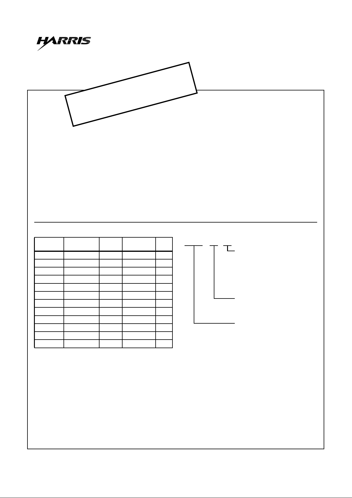
Part Number Information
PART
NUMBER CHANNELS
LOGIC
LEVEL PACKAGE
PKG
NO.
IH5009 4 +15 DD, PD
IH5010 4 +5 DD, PD
IH5011 4 +15 DE, PE
IH5012 4 +5 DE, PE
IH5014 3 +5 DD, PD
IH5016 3 +5 DE, PE
IH5017 2 +15 PA
IH5018 2 +5 DD, PA
IH5019 2 +15 DE, PA
IH5020 2 +5 DE, PA
IH5022 1 +5 DD, PA
IH5024 1 +5 PA
NOTE: Mil-Temperaturerange(-55oCto125oC)availableinceramic
packages only.
IH50XX M DE
PACKAGE
PA - 8 LEAD PDIP
PD - 14 LEAD PDIP
PE - 16 LEAD PDIP
DD - 14 LEAD CERDIP
DE - 16 LEAD CERDIP
TEMPERATURE RANGE
M = MILITARY (-55oC to 125oC)
C = COMMERCIAL (0oC to 70oC)
BASIC PART NUMBER
May 1999
CAUTION: These devices are sensitive to electrostatic discharge. Users should follow proper IC Handling Procedures.
Copyright
© Harris Corporation 1999
IH5009-5012, 5014,
5016-5020, 5022, 5024
Virtual Ground Analog Switch
File Number 3129.1
OBSOLETE PRODUCT
NO RECOMMENDED REPLACEMENT
Call Central Applications 1-800-442-7747
or email: centapp@harris.com
Page 2
4-2
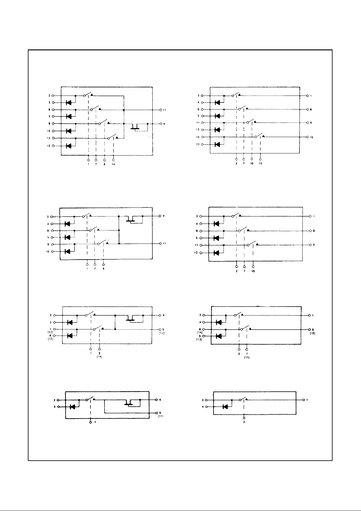
Functional Diagrams
(Numbers in brackets refer to CERDIP Packages)
IH5009, IH5010
(14 LEAD CERDIP, 14 LEAD PDIP)
IH5011, IH5012
(16 LEAD CERDIP, 16 LEAD PDIP)
IH5014
(14 LEAD CERDIP, 14 LEAD PDIP)
IH5016
(16 LEAD CERDIP, 16 LEAD PDIP)
IH5017 (8 LEAD PDIP)
IH5018 (8 LEAD PDIP, 14 LEAD CERDIP)
IH5019, IH5020
(8 LEAD PDIP, 16 LEAD CERDIP)
IH5022
(8 LEAD PDIP, 14 LEAD CERDIP)
IH5024
(8 LEAD PDIP)
IH5009 Series
Page 3

4-3
Absolute Maximum Ratings Thermal Information
Positive Analog Signal Voltage. . . . . . . . . . . . . . . . . . . . . . . . . . 30V
Negative Analog Signal Voltage . . . . . . . . . . . . . . . . . . . . . . . . .-15V
Diode Current. . . . . . . . . . . . . . . . . . . . . . . . . . . . . . . . . . . . . .10mA
Power Dissipation (Note) . . . . . . . . . . . . . . . . . . . . . . . . . . . 500mW
Operating Conditions
Temperature Range
5009C Series . . . . . . . . . . . . . . . . . . . . . . . . . . . . . . .0oC to 70oC
5009M Series . . . . . . . . . . . . . . . . . . . . . . . . . . . . -55oC to 125oC
Maximum Storage Temperature Range . . . . . . . . . .-65oC to 150oC
Maximum Lead Temperature (Soldering 10s). . . . . . . . . . . . . 300oC
CAUTION: Stresses above those listed in “Absolute Maximum Ratings” may cause permanent damage to the device. This is a stress only rating and operation
of the device at these or any other conditions above those indicated in the operational sections of this specification is not implied.
NOTE: Dissipation rating assumes device is mounted with all leads welded or soldered to printed circuit board in ambient temperature below
75oC. For higher temperature, derate at rate of 5m/WoC.
Electrical Specifications (Per Channel)
PARAMETER
(NOTE 1)
SYMBOL
(NOTE 4)
TEST
CONDITIONS
(NOTE 2)
TYPE
-55oC (M)
0oC (C)
MIN/MAX
25oC 125oC(M)
70oC (C)
MIN/MAX UNITSTYP MIN/MAX
Input Current-ON I
IN(ON)
ALL VIN = 0V, ID = 2mA - 0.01 ±0.5 100 µA
Input Current-OFF I
IN(OFF)
5V Logic Ckts VIN = +4.5V,
VA = ±10V
- 0.04 ±0.5 20 nA
Input Current-OFF I
IN(OFF)
15V Logic Ckts VIN = +11V,
VA = ±10V
- 0.04 ±0.5 20 nA
Channel Control
Voltage-ON
V
IN(ON)
5V Logic Ckts Note 3 0.5 - 0.5 0.5 V
Channel Control
Voltage-ON
V
IN(ON)
15V Logic Ckts Note 3 1.5 - 1.5 1.5 V
Channel Control
Voltage-OFF
V
IN(OFF)
5V Logic Ckts Note 3 - - 4.5 4.5 V
Channel Control
Voltage-OFF
V
IN(OFF)
15V Logic Ckts Note 3 - - 11.0 11.0 V
Leakage Current-OFF I
D(OFF)
5V Logic Ckts VIN = +4.5V,
VA = ±10V
- 0.02 ±0.5 20 nA
Leakage Current-OFF I
D(OFF)
15V Logic Ckts VIN = +11V,
VA = ±10V
- 0.02 ±0.5 20 nA
Leakage Current-ON I
D(ON)
5V Logic Ckts VIN = 0V, IS = 1mA - 0.30 ±1.0 1000 (M)
200 (C)
nA
Leakage Current-ON I
D(ON)
15V Logic Ckts VIN = 0V, IS = 1mA - 0.10 ±0.5 500 (M)
100 (C)
nA
Leakage Current-ON I
D(ON)
5V Logic Ckts VIN = 0V, IS = 2mA - - 1.0 10 µA
Leakage Current-ON I
D(ON)
15V Logic Ckts VIN = 0V, IS = 2mA - - 2.0 100 µA
Drain-Source
ON-Resistance
r
DS(ON)
5V Logic Ckts ID = 2mA, VIN = 0.5V 150 90 150 385 (M)
240 (C)
Ω
Drain-Source
ON-Resistance
r
DS(ON)
15V Logic Ckts ID = 2mA, VIN = 1.5V 100 80 100 250 (M)
160 (C)
Ω
Turn-ON Time t
(ON)
All - 150 500 - ns
Turn-OFF Time t
(OFF)
All - 300 500 - ns
Cross Talk CT All f = 100Hz - 120 - - dB
NOTES:
1. (OFF) and (ON) subscript notation refers to the conduction state of the FET switch for the given test.
2. Refer to Figure 1 for definition of terms.
3. V
IN(ON)
and V
IN(OFF)
are test conditions guaranteed by the tests of r
DS(ON)
and I
D(OFF)
respectively.
4. “5V Logic CKTS” applies to even-numbered devices. “15V Logic CKTS” applies to odd-numbered devices.
IH5009 Series
 Loading...