

Page 1
查询IH5043CPE供应商
TM
ODUCT
ODUCT
OBSOLETE PR
Data Sheet March 2000
POSSIBLE SUBSTITUTE PR
HI-5043
IH5043
File Number 3130.3
[ /Title
(IH504
3)
/Subject
(Dual
SPDT
CMOS
Analog
Switch
)
/Autho
r ()
/Keywords
(Intersil
Corporation,
semiconductor,
Dual
SPDT
CMOS
Analog
Switch
)
/Creator ()
/DOCI
NFO
pdfmark
[
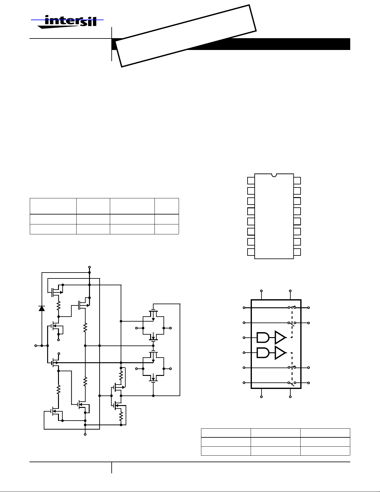
Dual SPDT CMOS Analog Switch
The IH5043 analog switch uses an improved, high voltage
CMOS monolithic technology. These devices provide ease
of use and performance advantages not previously
available from solid state switches.
Key performance advantage is TTL compatibility and ultra
low power operation. The quiescent current requirement is
less than 1mA. Also, the IH5043 guarantees Break-BeforeMake switching, accomplished by extending the t
(300ns Typ), so that it exceeds t
time (200ns Typ). This
OFF
ON
time
insures that an ON channel will be turned OFF before an
OFF channel can turn ON. The need for external logic
required to avoid channel to channel shorting during
switching is eliminated.
Part Number Information
TEMP.
PART NUMBER
IH5043CPE 0 to 70 16 Ld PDIP E16.3
IH5043CY 0 to 70 16 Ld SOIC M16.15
RANGE (oC) PACKAGE
PKG.
NO.
Schematic Diagram
FUNCTIONAL DRIVER,TYPICAL DRIVER, GATE (1/2AS SHOWN)
V+
Q
3
5K
Q
1
IN
GND
V
L
Q
2
10K
Q
5
Q
4
2K
400Ω
1K
Q
6
400Ω
V-
S
1
S
3
Q
7
Q
8
FLOATS
FLOATS
Q
9
Q
10
Q
11
Q
12
Features
• See HI504X for Other Functions
• Dual SPDT
• Switches Greater than 20V
Signals with ±15V Supplies
P-P
• Quiescent Current Less than 1mA
• Break-Before-Make Switching t
200ns, tON 300ns (Typ)
OFF
• TTL, DTL, CMOS, PMOS Compatible
Pinout
D
NC
D
S
S
D
NC
D
1
3
3
4
4
2
(PDIP, SOIC)
1
2
3
4
5
6
7
8
IH5043
TOP VIEW
16
S
1
15
IN
1
14
VGND
13
V
12
L
11
V+
IN
10
2
9
S
2
Functional Diagram
V
L
12 11
16
S
1
4
S
D
1
D
3
LOGIC SWITCH 1, 2 SWITCH 3, 4
3
15
IN
1
10
IN
2
9
S
2
5
S
4
13 14
GND
SWITCH STATES SHOWN ARE FOR LOGIC “1” INPUT
TRUTH TABLE
0 Off On
1 On Off
V+
V-
1
D
1
3
D
3
8
D
2
6
D
4
1
1-888-INTERSIL or 321-724-7143 | Intersil and Design is a trademark of Intersil Corporation. | Copyright © Intersil Corporation 2000
CAUTION: These devices are sensitive to electrostatic discharge; follow proper IC Handling Procedures.
Page 2
IH5043
Absolute Maximum Ratings Thermal Information
V+ to V- . . . . . . . . . . . . . . . . . . . . . . . . . . . . . . . . . . . . . . . . . . <36V
V+ to VD. . . . . . . . . . . . . . . . . . . . . . . . . . . . . . . . . . . . . . . . . . <30V
VD to V- . . . . . . . . . . . . . . . . . . . . . . . . . . . . . . . . . . . . . . . . . . <30V
VD to VS. . . . . . . . . . . . . . . . . . . . . . . . . . . . . . . . . . . . . . . . . .<±22V
VL to V- . . . . . . . . . . . . . . . . . . . . . . . . . . . . . . . . . . . . . . . . . . <33V
VL to VIN . . . . . . . . . . . . . . . . . . . . . . . . . . . . . . . . . . . . . . . . . <30V
VL to GND . . . . . . . . . . . . . . . . . . . . . . . . . . . . . . . . . . . . . . . . <20V
VIN to GND . . . . . . . . . . . . . . . . . . . . . . . . . . . . . . . . . . . . . . . <20V
Continuous Current (S-D) . . . . . . . . . . . . . . . . . . . . . . . . . . . . 30mA
Peak Current S-D (Pulsed 1ms, 10% Duty Cycle Max). . . . . . 70mA
Operating Conditions
Temperature Range. . . . . . . . . . . . . . . . . . . . . . . . . . . 0oC to 70oC
CAUTION: Stresses above those listed in “Absolute Maximum Ratings” may cause permanent damage to the device. This is a stress only rating and operation of the
device at these or any other conditions above those indicated in the operational sections of this specification is not implied.
NOTE:
1. θJA is measured with the component mounted on an evaluation PC board in free air.
Thermal Resistance (Typical, Note 1) θJA (oC/W)
PDIP Package . . . . . . . . . . . . . . . . . . . . . . . . . . . . . 90
SOIC Package . . . . . . . . . . . . . . . . . . . . . . . . . . . . . 115
Maximum Junction Temperature (Plastic Packages) . . . . . . .150oC
Maximum Storage Temperature. . . . . . . . . . . . . . . . -65oC to 150oC
Maximum Lead Temperature (Soldering 10s) . . . . . . . . . . . . 300oC
(SOIC - Lead Tips Only)
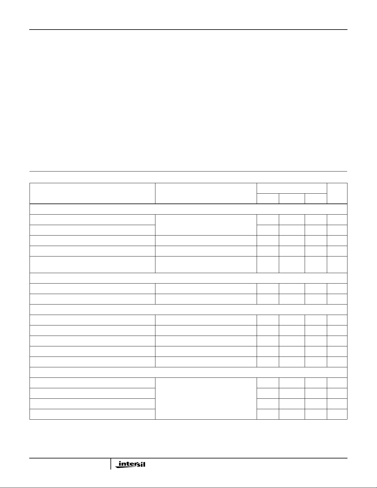
Electrical Specifications V+ = +15V, V- = -15V, V
= +5V
L
(NOTES 2, 3)
PER CHANNEL PARAMETER TEST CONDITIONS
UNITS0oC25oC70oC
DYNAMIC CHARACTERISTICS
Turn ON Time, t
Turn OFF Time, t
ON
OFF
RL = 1kΩ, V
Figure 6
ANALOG
= -10V to +10V, See
- 1000 - ns
- 500 - ns
Charge Injection, Q See Figure 7 - 20 (Typ) - mV
OFF Isolation, OIRR f = 1MHz, RL= 100Ω,CL≤ 5pF, See Figure 4 - 50 (Typ) - dB
Crosstalk, CCRR One Channel Off; Any Other Channel
- -50 (Typ) - dB
Switches as per Figure 3
DIGITAL INPUT CHARACTERISTICS
Input Logic Current, I
Input Logic Current, I
IN(ON)
IN(OFF)
VIN = 2.4V ±1 ±110µA
VIN = 0.8V ±1 ±110µA
ANALOG SWITCH CHARACTERISTICS
Drain-Source ON Resistance, r
Channel-to-Channel r
DS(ON)
DS(ON)
Match, ∆r
DS(ON)
Minimum Analog Signal Handling Capability, V
Switch OFF Leakage Current, I
Switch ON Leakage Current, I
, I
D(OFF)
D(ON)+IS(ON)
S(OFF)
ANALOG
IS = 10mA, V
ANALOG
= -10V to +10V 80 80 130 Ω
- 30 (Typ) - Ω
- ±10 (Typ) - V
V
= -10V to +10V - ±5 100 nA
ANALOG
VD = VS = -10V to +10V - ±10 100 nA
POWER SUPPLY CHARACTERISTICS
+ Power Supply Quiescent Current, I+ 10 10 100 µA
- Power Supply Quiescent Current, I- 10 10 100 µA
+5V Supply Quiescent Current, I
Ground Quiescent Current, I
GND
L
10 10 100 µA
10 10 100 µA
NOTES:
2. Typical values are for design aid only, not guaranteed and not subject to production testing.
3. Min or Max value unless otherwise specified.
2
Page 3
Test Circuits and Waveforms
IH5043
100
80
(Ω)
60
DS(ON)
r
40
20
0
-10.0 -5.0 -2.5 0 2.5 5.0 7.5 10.0-7.5
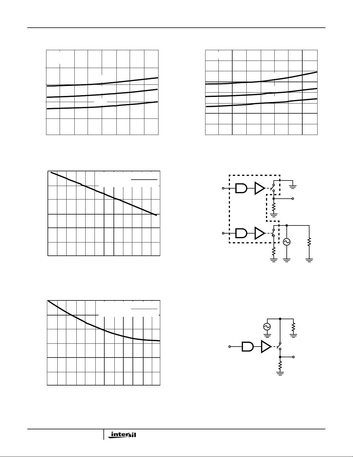
FIGURE 1. r
-120
-100
-80
-60
IS = 1mA
= ±15V
V
S
125oC
25oC
-55oC
V
vs ANALOG INPUT VOLTAGE FIGURE 2. r
DS(ON)
(V)
ANALOG
CCRR = 20LOG
V
OUT
2000mV
(mV
P-P
P-P
)
(Ω)
DS(ON)
r
160
140
120
100
80
60
40
20
0
-10.0 -5.0 -2.5 0 2.5 5.0 7.5 10.0-7.5
IS = 1mA
OFF
STATE
VS = ±10V
VS = ±12V
VS = ±15V
V
vs POWER SUPPLY VOLTAGE
DS(ON)
ANALOG
(V)
100Ω
V
OUT
-40
CROSSTALK (dB)
-20
0
1 10 100 1K 10K 100K 1M
FREQUENCY (Hz)
ON
STATE
FIGURE 3A. CROSSTALK vs FREQUENCY FIGURE 3B. TEST CIRCUIT
FIGURE 3. CROSSTALK
120
100
80
60
40
OFF ISOLATION (dB)
20
0
1 10 100 1K 10K 100K 1M
OIRR = 20LOG
FREQUENCY (Hz)
2000mV
V
OUT
(mV
P-P
P-P
)
AT 1MHz
OFF STATE
2V
P-P
100Ω
2V
AT 1MHz
100Ω
P-P
51Ω
V
51Ω
OUT
FIGURE 4A. OFF ISOLATION vs FREQUENCY FIGURE 4B. TEST CIRCUIT
FIGURE 4. OFF ISOLATION
3
Page 4
Test Circuits and Waveforms (Continued)
IH5043
3V
0V
0.1T
1000
100
10
(EITHER + OR - SUPPLY) (µA)
QUIESCENT
0
I
1 10 100 1K 10K 100K
LOGIC FREQUENCY AT 10% DUTY CYCLE (Hz)
LOGIC INPUT
T
3V
0V
LOGIC
INPUT
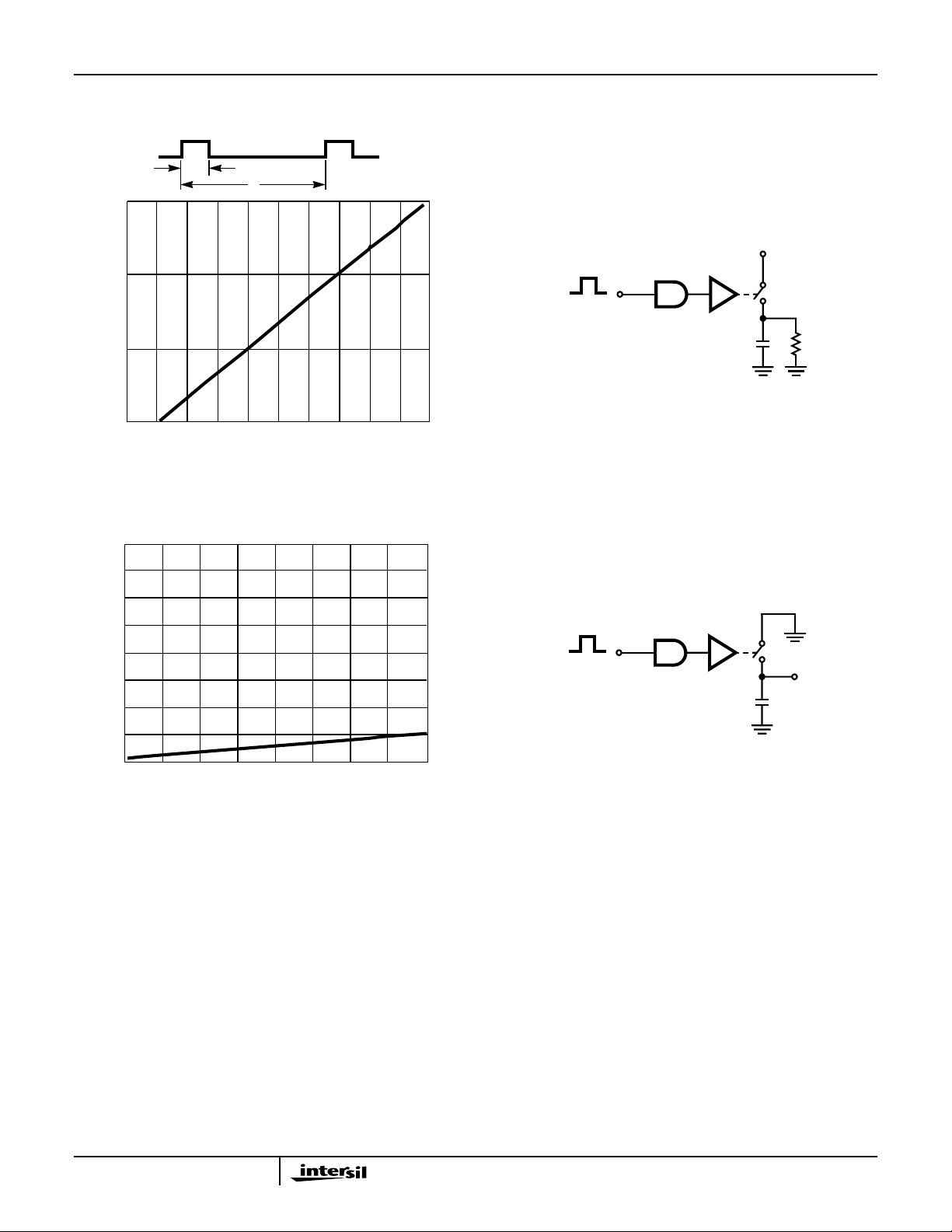
FIGURE 5. SUPPLY CURRENT vs LOGIC FREQUENCY FIGURE 6. tON AND t
45
40
ANALOG INPUT
10pF
TEST CIRCUIT
OFF
10V
V
1kΩ
OUT
35
)
P-P
30
(mV
25
20
INJECT
Q
15
10
0
-10.0 -5.0 -2.5 0 2.5 5.0 7.5 10.0-7.5
V
ANALOG
3V
0V
LOGIC
INPUT
(V)
ANALOG INPUT
10nF
FIGURE 7A. CHARGE INJECTION vs ANALOG INPUT VOLTAGE FIGURE 7B. TEST CIRCUIT
FIGURE 7. CHARGE INJECTION
V
OUT
4
Page 5
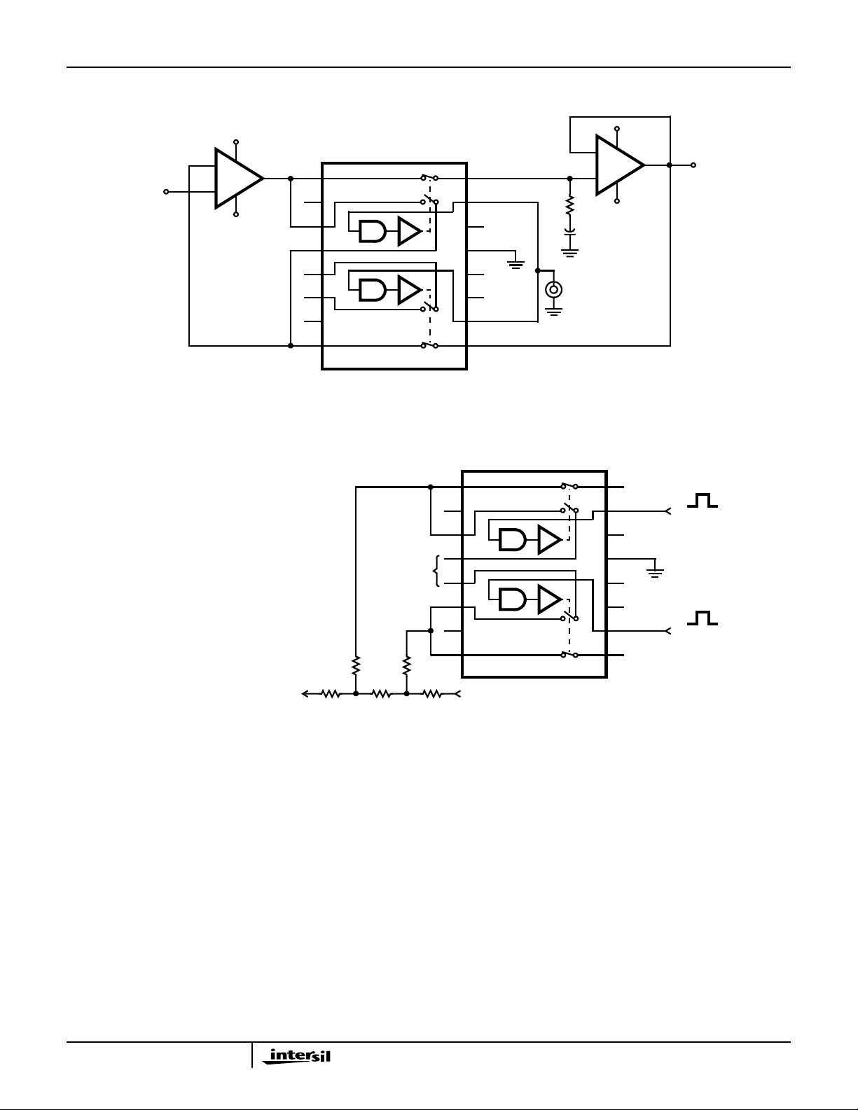
Typical Applications
IH5043
+15V
7
ANALOG
INPUT
EXAMPLE: If -V
+V
ANALOG
= +10VDC, then Ladder Legs
2
CA741
3
-15V
ANALOG
6
4
= -10VDCand
1
2
3
4
5
6
7
8
are switchedbetween ±10VDC, depending
upon state of Logic Strobe.
ETC.
16
15
14
-15V
13
12
+5V
11
+15V
10
9
IH5043
+3V = SAMPLE MODE
0V = HOLD MODE
FIGURE 8. IMPROVED SAMPLE AND HOLD
1
2
3
4
-V
ANALOG
2R
RR
2R
5
6
7
8
IH5043
R
ETC.
51Ω
LOGIC INPUT
+15V
7
2
CA5420
3
4
-15V
10,000pF
POLYSTYRENE
16
+V
15
14
-15V
13
12
+5V
11
+15V
10
9
+V
6
ANALOG
T2L LOGIC
STROBE
T2L LOGIC
ANALOG
STROBE
0V = HOLD MODE
OUTPUT
FIGURE 9. USING THE CMOS SWITCH TO DRIVE AN R/2R LADDER NETWORK (2 LEGS)
5
Page 6
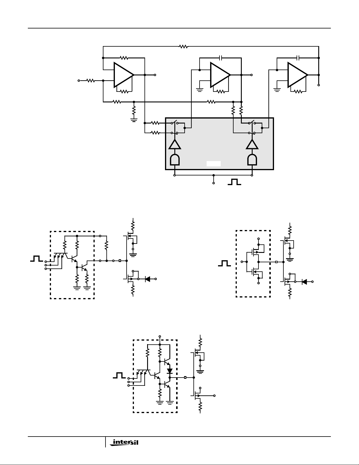
Typical Applications (Continued)
IH5043
100kΩ
-
CA3440
+
3M
100kΩ
1kΩ
SIGNAL
INPUT
100kΩ
Constant gain, constant Q, variable frequency
filter which provides simultaneous Lowpass,
Bandpass, and Highpass outputs. With the
component values shown, center frequency will
be 235Hz and 23.5Hz for high and low logic
inputs respectively, Q = 100, and Gain = 100.
f
Center Frequency
N
1
-----------------==
2π RC
FIGURE 10. DIGITALLY TUNED LOW POWER ACTIVE FILTER
HI PASS
OUTPUT
68kΩ
R
680kΩ
R
100kΩ
10,000pF
-
CA3440
+
3M
100kΩ
680kΩ
IH5043
C
3V
0V
LOGIC STROBE
R
BANDPASS
68kΩ
R
OUTPUT
10,000pF
C
-
CA3440
+
3M
LO PASS
OUTPUT
R
EXT
(1kΩ TO
20kΩ)
LOGIC
INPUT
10kΩ
IN
20kΩ
GND
V
L
1N914
V+
+15V
T2L
LOGIC
15V TTL GATE
FIGURE 11. INTERFACING WITH TTL OPEN COLLECTOR
LOGIC (TYP EXAMPLE FOR +15V CASE SHOWN)
T2L
LOGIC
5V TTL GATE
+15V
+5V
IN
10kΩ
IN
20kΩ
V-
15V ≥ V+ ≥ 5V
0V ≥ V- ≥ -15V
V+
V+
V-
CMOS GATE
FIGURE 12. INTERFACING WITH CMOS LOGIC
5kΩ
GND
+5V
V
L
V+
+15V OR +V
(VI TERMINAL)
10Ω
CC
GND
V
L
V
V+
DD
FIGURE 13. TTL LOGIC INTERFACE
6
Page 7
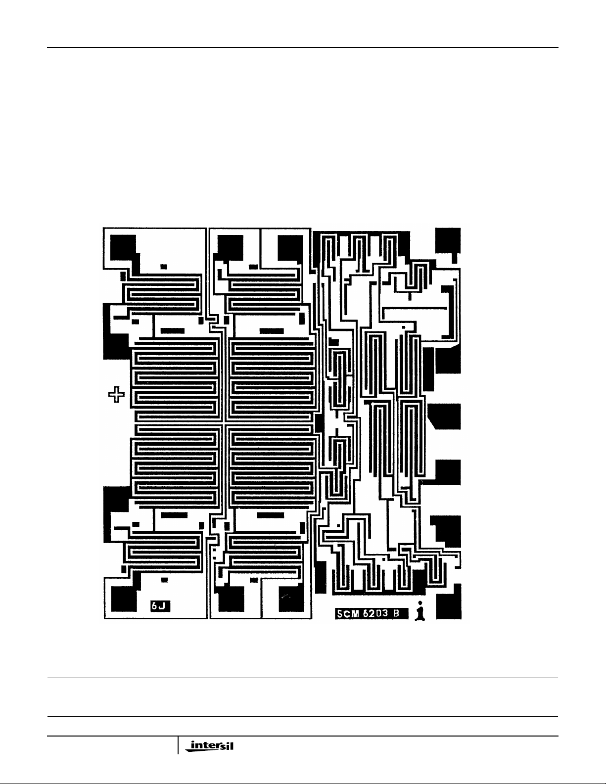
Die Characteristics
IH5043
DIE DIMENSIONS:
1778µm x 1905µm
METALLIZATION:
Type: Al
Thickness: 10k
Å ±1kÅ
Metallization Mask Layout
D
3
S
3
PASSIVATION:
Type: PSG/Nitride
PSG Thickness: 7k
Å ±1.4kÅ
Nitride Thickness: 8kÅ ±1.2kÅ
WORST CASE CURRENT DENSITY:
4
2
9.1 x 10
IH5043
D
1
S
1
A/cm
IN
1
V-
GND
V
L
S
4
V+
(SUBSTRATE)
D
4
D
2
S
2
IN
2
All Intersil semiconductor products are manufactured, assembled and tested under ISO9000 quality systems certification.
Intersil semiconductor products are sold by description only.Intersil Corporation reserves the rightto makechanges in circuit design and/or specifications at any time without notice. Accordingly, the reader is cautioned to verify that data sheets are current before placing orders. Information furnished by Intersil is believ edto be accurate and
reliable. However, no responsibility is assumed by Intersil or its subsidiaries for its use; nor forany infringements of patents or other rights of third parties which mayresult
from its use. No license is granted by implication or otherwise under any patent or patent rights of Intersil or its subsidiaries.
For information regarding Intersil Corporation and its products, see web site www.intersil.com
7
 Loading...