

Page 1
Integrated
Circuit
Systems, Inc.
General Description Features
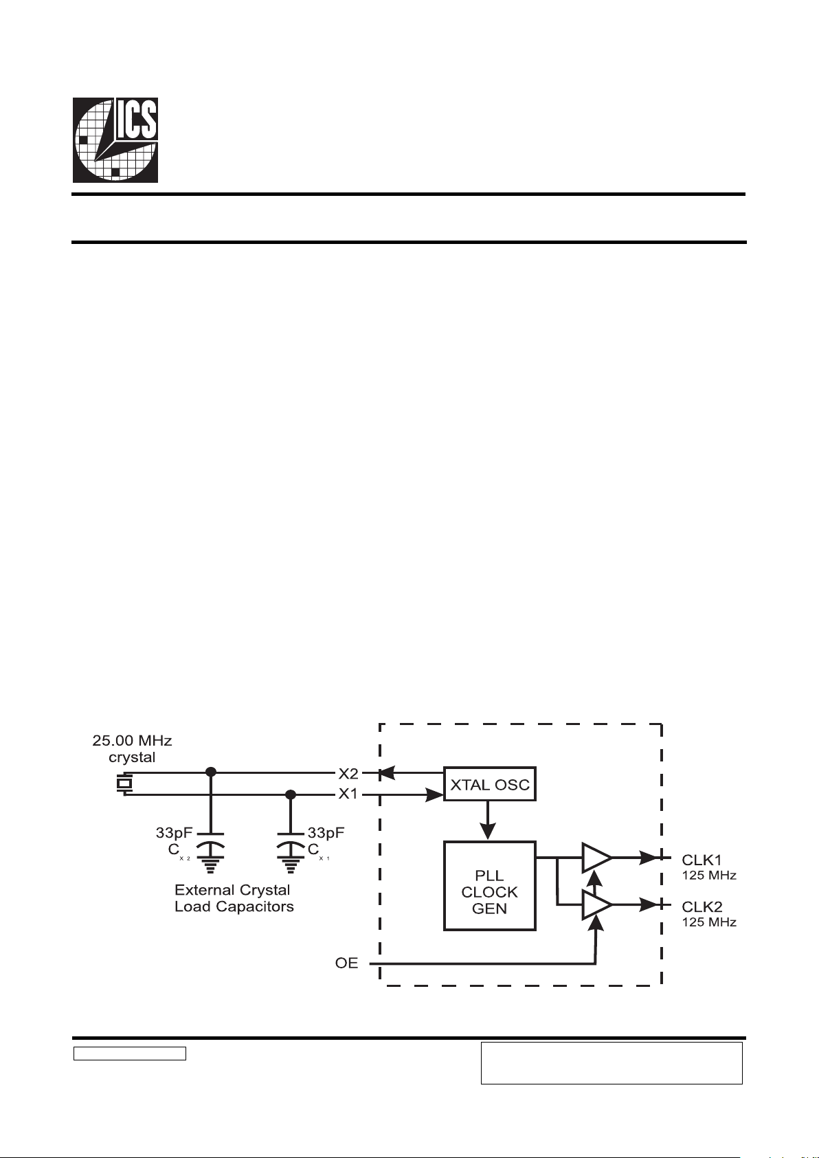
ICS91 12-41/42
Block Diagram
Frequency Generator for Gigabit Ethernet Systems
Applications
ICS9112-41/42 Rev D 3/3/99
The ICS9112-41/42 is a high speed clock generator designed
to support Gigabit Ethernet system requirements. The ICS91 12-
41/42 generates 125 MHz from a 25 MHz crystal.
An exact frequency multiplying ratio ensures better than ±100
ppm frequency accuracy using a standard AT crystal with
external load capacitors (typically 33pF±5% for an 18pF load
crystal). Achieving ±100 ppm over four years requires the
crystal to have a ±20 ppm initial accuracy , ±30 ppm temperature
and ±5 ppm/year aging coefficients.
The ICS9112-41/42 with less than 25ps accumulative jitter is
well suited for Gigabit Ethernet applications.
• Generates 125 MHz clocks from a 25 MHz crystal
• Less than 45ps one sigma jitter (15ps typ.)
• Less than ±130ps absolute jitter
• Less than 25ps accumulative jitter @ 256 cycles
• Rise/fall times less than 1.2ns driving 15pF
• On-chip loop filter components
• 3.0V-5.5V supply range
• 8-pin, 150-mil SOIC package
• Specifically designed to support the high-speed
clocking requirements of Gigabit Ethernet systems.
PRODUCT PREVIEW documents contain information on new
products in the sampling or preproduction phase of development.
Characteristic data and other specifications are subject to change
without notice.
Preliminary Product Preview
Page 2

2
ICS9112-41/42
Preliminary Product Preview
Pin Descriptions
Pin Configurations
8-Pin SOIC
Functionality
EO
2X,1X
)zHM(
TUOF
)zHM(
100.52521
000.52etatsirT
8-Pin SOIC
NIP
REBMUN
EMANNIPEPYTNOITPIRCSED
1DNGARWP.dnuorggolanA
2DNGWRP.dnuorGlatigiD
31XNI .sroticapacdaollanretxeseriuqeR.zHM0.52yllanimon;ecivedottupnikcolcrolatsyrC
42XNI.sroticapacdaollanretxeseriuqeR.ecivedmorftuptuoevirdlatsyrC
5EONI )TUOF(tuptuokcolcehtsetatsirtti,wolsiEOnehw:).pu_lluplanretnisah(elbanetuptuO
6
DDVRWP)14(.ylppustlov0.5+ro3.3+
2KLCTUO)24(.zHM521tuptuokcolc
7
DDVARWP)14(.)egatlovrewoplatigidlauqetsuM(.rewopgolanA
DDVA+DDVRWP)24(.ylppustlov0.5+ro3.3+,rewopgolanadnalatigiD
81KLCTUO.zHM521tuptuokcolC
Page 3

3
ICS9112-41/42
Preliminary Product Preview
Note 1: Parameter is guaranteed by design and characterization. Not 100% tested in production.
Electrical Characteristics at 5.0V
Operating VDD = +4.5V to +5.5V; TA =0°C to 70°C unless otherwise stated
Absolute Maximum Ratings
AVDD, VDD referenced to GND . . . . . . . . . . . . . . . 7V
Operating temperature under bias. . . . . . . . . . . . . . . . 0°C to +70°C
Storage temperature . . . . . . . . . . . . . . . . . . . . . . . . . . -65°C to +150°C
Voltage on I/O pins referenced to GND. . . . . . . . . . . GND -0.5V to VDD +0.5V
Power dissipation . . . . . . . . . . . . . . . . . . . . . . . . . . . . 0.5 Watts
Stresses above those listed under Absolute Maximum Ratings may cause permanent damage to the device.
This is a stress rating only and functional operation of the device at these or any other conditions above
those indicated in the operational sections of the specifications is not implied. Exposure to absolute
maximum rating conditions for extended periods may affect product reliability.
scitsiretcarahCCD
RETEMARAPLOBMYSSNOITIDNOCTSETNIMPYTXAMSTINU
egatloVwoLtupnIV
LI
-- 8.0V
egatloVhgiHtupnIV
HI
0.2--V
tnerruCwoLtupnII
LI
V
NI
)tupnipu-lluP(V0=0.61-0.6--Aµ
tnerruChgiHtupnII
HI
VNIV=
DD
0.2--0.2Aµ
egatloVwoLtuptuO
1
V
LO
I
LO
Am01=-51.004.0V
egatloVhgiHtuptuO
1
V
HO
I
HO
Am03-=4.252.3-V
tnerruCwoLtuptuO
1
I
LO
V
LO
V8.0=0.220.53-Am
tnerruChgiHtuptuO
1
I
HO
V
HO
V0.2=-0.05-0.53-Am
tnerruCylppuSI
DD
dedaolnU-0.220.54Am
rotsiseRpu-lluP
1
R
up
-001- smhok
scitsiretcarahCCA
emiTesiR
1
T
1r
V0.2ot8.0,daolFp51-8.02.1sn
emiTllaF
1
T
1f
V8.0ot0.2,daolFp51-7.02.1sn
elcyCytuD
1
D
t
V4.1@daolFp510.240.940.55%
amgiSenO,rettiJ
1
T
s1j
daolFp51-0.510.54sp
etulosbA,rettiJ
1
T
baj
daolFp510.031-0.031sp
rettiJevitalumuccA
1
T
ccaj
elcyC652@daolFp51-0.71-sp
ycneuqerFtupnI
1
F
i
-0.52-zHM
ycneuqerFtuptuO
1
F
o
-521- zHM
emiTpu-rewoP
1
T
up
-85.70.81sm
ecnaticapaCtupnIlatsyrC
1
C
xni
)1niP(1X
)8niP(2X
-0.3-Fp
Page 4
4
ICS9112-41/42
Preliminary Product Preview
Electrical Characteristics at 3.3V
Note 1: Parameter is guaranteed by design and characterization. Not 100% tested in production.
Operating V
DD
= +3.0V to +3.7V; TA =0°C to 70°C unless otherwise stated
scitsiretcarahCCD
RETEMARAPLOBMYSSNOITIDNOCTSETNIMPYTXAMSTINU
egatloVwoLtupnIV
LI
-- V02.0
DD
V
egatloVhgiHtupnIV
HI
V7.0
DD
--V
tnerruCwoLtupnII
LI
V
NI
)tupnipu-lluP(V0=0.7-5.2--Aµ
tnerruChgiHtupnII
HI
VNIV=
DD
0.2--0.2Aµ
egatloVwoLtuptuO
1
V
LO
I
LO
Am6=-V50.0
DD
V1.0
DD
V
egatloVhgiHtuptuO
1
V
HO
I
HO
Am5-=V58.0
DD
V29.0
DD
-V
tnerruCwoLtuptuO
1
I
LO
V
LO
V2.0=
DD
0.510.22-Am
tnerruChgiHtuptuO
1
I
HO
V
HO
V7.0=
DD
-0.71-0.01-Am
tnerruCylppuSIDDdedaolnU-0.410.03Am
rotsiseRpu-lluP
1
R
up
-0.571- smhok
scitsiretcarahCCA
emiTesiR
1
T
1r
V0.2ot8.0,daolFp51-57.02.1sn
emiTllaF
1
T
1f
V8.0ot0.2,daolFp51-7.02.1sn
elcyCytuD
1
D
t
V4.1@daolFp510.040.050.06%
amgiSenO,rettiJ
1
T
s1j
daolFp51-0.510.54sp
etulosbA,rettiJ
1
T
baj
daolFp510.031--0.031sp
rettiJevitalumuccA
1
T
ccaj
elcyc652@daolFp51-0.71-sp
ycneuqerFtupnI
1
F
i
-0.52-zHM
ycneuqerFtuptuO
1
F
o
-52.601-zHM
emiTpu-rewoP
1
T
up
-85.70.81sm
ecnaticapaCtupnIlatsyrC
1
C
xni
)1niP(1X
)8niP(2X
-0.3-Fp
Page 5
5
ICS9112-41/42
Preliminary Product Preview
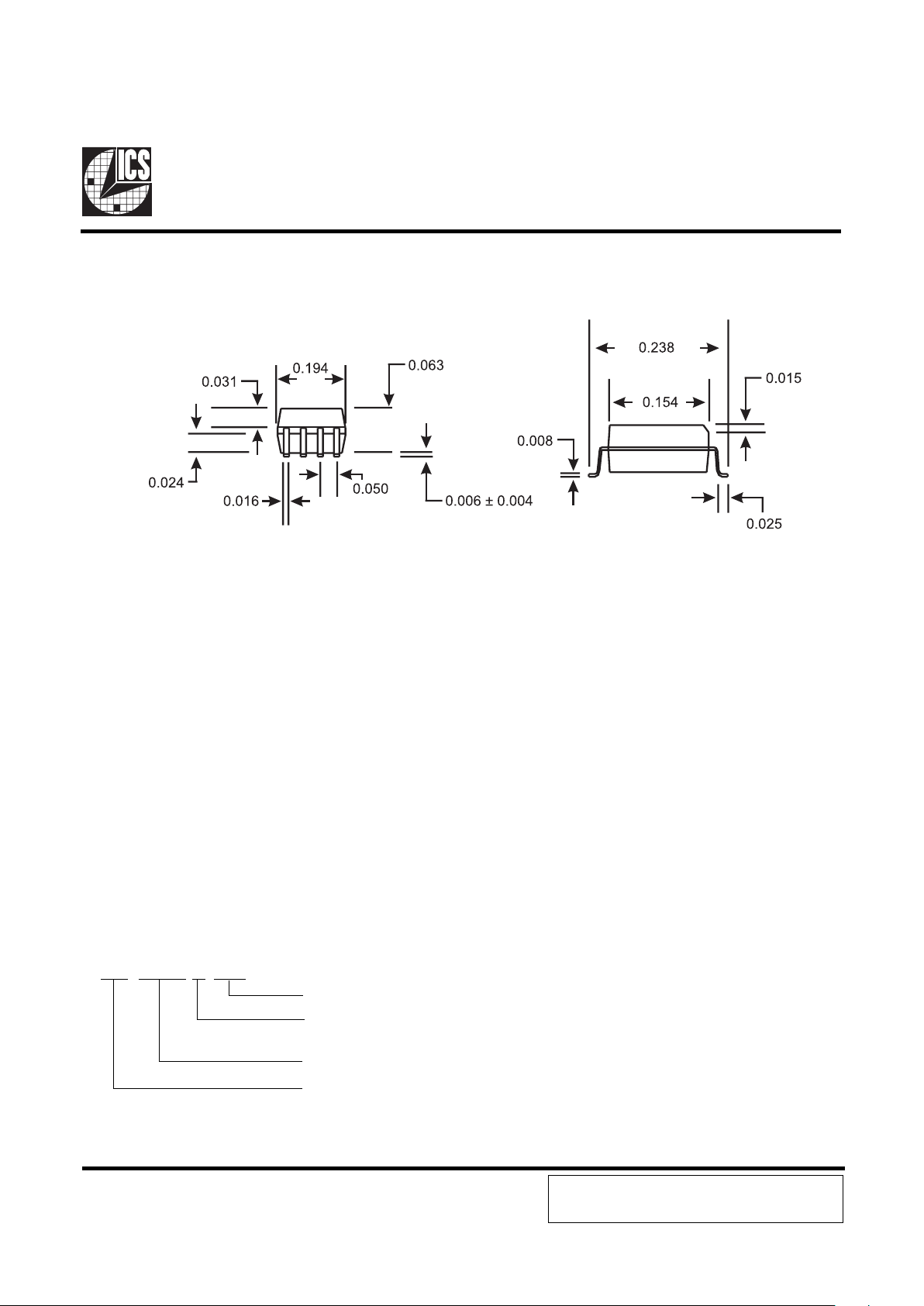
8-Pin Plastic SOIC Package
ICS XXXX M-PPP
Example:
Package T ype
M=SOIC, SOP
Device T ype (consists of 3 or 4 digit numbers)
ICS=Standard Device
Prefix
Ordering Information
ICS9112M-41/42
Pattern Number(2 or 3 digit number for parts with ROM code patterns)
PRODUCT PREVIEW documents contain information on new
products in the sampling or preproduction phase of development.
Characteristic data and other specifications are subject to change
without notice.
 Loading...