

Datasheet AVS9107C-03CS14, AV9107C-11CS14, AV9107C-10CS08, AV9107C-03CS14, ICS9107C-05CS08 Datasheet (ICST)
...Page 1
Integrated
Circuit
Systems, Inc.
General Description
Features
AV9107C
ICS reserves the right to make changes in the device data identified in this
publication without further notice. ICS advises its customers to obtain the latest
version of all device data to verify that any information being relied upon by the
customer is current and accurate.
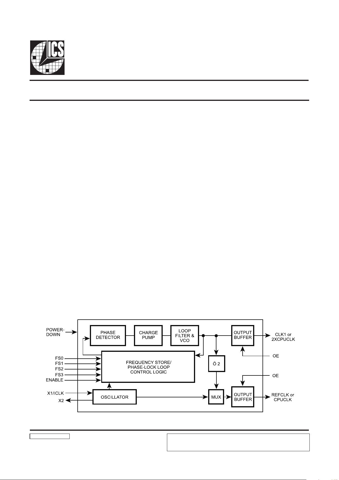
The AV9107C offers a tiny footprint solution for generating
two simultaneous clocks. One clock, the REFCLK, is a fixed
output frequency which is the same as the input reference
crystal (or clock). The other clock, CLK1, can vary between 2
and 120 MHz, with up to 16 selectable preprogrammed frequencies stored in internal ROM (frequency range depends on
design option).
The device has advanced features which include on-chip loop
filters, tristate outputs, and power-down capability. A minimum of external components - two decoupling capacitors and
an optional ferrite bead - are all that are required for jitter-free
operation. Standard versions for computer motherboard applications are the AV9107C-03, and AV9107C-05. Custom masked
versions, with customized frequencies and features, are available
in 6-8 weeks for a small NRE.
Patented on-chip Phase-Locked Loop with VCO for
clock generation
Provides reference clock and synthesized clock
Generates frequencies from 2 to 120 MHz (depending
on option), operates to 80 MHz for VDD 3.3V±10%
8-pin DIP or SOIC package or 14-pin DIP or SOIC
package
2 to 32 MHz input reference frequency (depending on
option)
On-chip loop filter
Up to 16 frequencies stored internally
Low power CMOS technology
Single +3.3 or +5 volt power supply
9107 C Rev D 2/3/98
Block Diagram
CPU Frequency Generator
Applications
Graphics: The AV9107C is the easiest to use, lowest cost,
and smallest footprint frequency generator for graphics
applications. It can generate up to 16 different frequencies,
including all frequencies necessary for VGA standards. It
should be used in place of the AV9105/6 when the reference
clock is also needed.
Computer: The AV9107C is the ideal solution for replacing
high speed oscillators and for reducing clock speeds to save
power in computers. The device provides smooth, glitchfree frequency transitions so that the CPU can continue to
operate during slow down or speed up. The rate of
frequency change makes the AV9107C compatible with all
386DX, 386SX, 486DX, 486DX2, and 486SX devices.
Standard versions include the AV9107C-03, -05, -10,
-11. Disk Drives: Smaller than a single crystal or an
oscillator, the tiny SOIC package can be used for any
general purpose frequency generation in disk drives.
Pentium is a trademark of Intel Corporation
PowerPC is a trademark of Motorola Corporation
Page 2
2
AV9107C
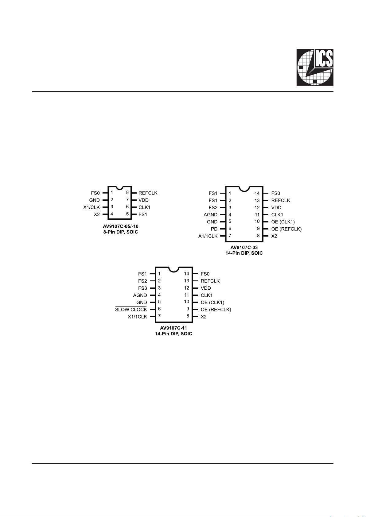
Pin Configuration
Applications (cont.)
The most popular application is for Constant Density
Recording, where its low jitter output clock provides the
necessary frequencies for reading and recording. Another
popular application is for slowing the disk drive CPU to
save power.
High Speed Systems: TheAV9107C can be used as a
proximity oscillator - using a low frequency (down to 2
MHz) input to generate a high frequency clock (up to 120
MHz) near the device requiring the high frequency
(depending on option). This avoids the need to route high
speed traces over a long distance.
Page 3
3
AV9107C
SLOW CLOCK FS3 FS2 FS1 FS0 CLK1
1
1
1
1
1
1
1
1
1
1
1
1
1
1
1
1
0
0
0
0
1
0
0
0
0
1
1
1
1
1
1
1
1
1
0
0
0
0
1
1
1
1
0
0
0
0
1
1
1
1
1
0
0
1
1
0
0
1
1
0
0
1
1
0
0
1
1
1
0
1
0
1
0
1
0
1
0
1
0
1
0
1
0
0
1
16.00 MHz
39.99 MHz
50.11 MHz
80.01 MHz
66.58 MHz
100.23 MHz*
8.02 MHz
4.01 MHz
8.02 MHz
20.00 MHz
25.06 MHz
39.99 MHz
33.25 MHz
50.11 MHz
30.00 MHz
4.01 MHz
8.05 MHz
Actual Frequencies
Decoding Table for AV9107C-05, 14.318 MHz input
Decoding Table for AV9107C-10, 14.318 MHz input
*@ VDD=5 volts
Decoding Table for AV9107C-03, 14.318 MHz input
Decoding Table for AV9107C-11 (in MHz)
*@ VDD=5 volts
FS1 FS0 CLK1
0
0
1
1
0
1
0
1
25.06 MHz
33.29 MHz
40.00 MHz
50.11 MHz
FS1 FS0 CLK1
0
0
1
1
0
1
0
1
40.01 MHz
50.11 MHz
66.61 MHz
80.01 MHz
FS3 FS2 FS1 FS0 CLK1
0
0
0
1
0
0
0
0
1
1
1
1
1
1
1
1
0
0
0
0
1
1
1
1
0
0
0
0
1
1
1
1
0
0
1
1
0
0
1
1
0
0
1
1
0
0
1
1
0
1
0
1
0
1
0
1
0
1
0
1
0
1
0
1
16.00 MHz
39.99 MHz
50.11 MHz
80.01 MHz
66.58 MHz 100.23
MHz* 8.02 MHz
4.01 MHz
8.02 MHz
20.00 MHz
25.06 MHz
40.01 MHz
33.29 MHz
50.11 MHz*
4.01 MHz
2.05 MHz
Page 4

4
AV9107C
PIN NUMBER
PIN NAME TYPE DESCRIPTION
-05/-10 -03 -11
1 14 14 FS0 Input Frequency Select 0 for CLK1 (-03 and -11 have pull-ups).
5 1 1 FS1 Input Frequency Select 1 for CLK1 (-03 and -11 have pull-ups).
2 2 FS2 Input Frequency Select 2 for CLK1 (-03 and -11 have pull-ups).
3 3 FS3 Input Frequency Select 3 for CLK1 (-03 and -11 have pull-ups).
4 4 AGND - Analog GROUND.
2 5 5 GND - Digital GROUND.
6 PD Input POWER-DOWN. Shuts off chip when low. Internal pull-up.
6 SLOW CLOCK Input SLOW CLOCK input. Forces CLK1 to 8 MHz (regardless of
FS condition). Has internal pull-up.
3 7 7 X1/ICLK Input CRYSTAL OUTPUT or INPUT CLOCK frequency. Typically
14.318 MHz system clock. This input includes load
capacitance and feedb ack bias for a crystal.
4 8 8 X2 Output CRYSTAL OUTPUT (No Connect when clock used.) This
input includes XTAL load capacitance.
9 9 OE(REFCLK) Input OUTPUT ENABLE. Tristates REFCLK when low. Has
internal pull-up.
10 10 OE(CLK1) Input OUTPUT ENABLE. Tristates CLK1 when low. Has internal
pull-up.
6 11 11 CLK1 Output CLOCK1 Output (see decoding tables).
7 12 12 VDD - Digital power supply.
8 13 13 REFCLK Output REFERENCE CLOCK output. Produces a buffered version of
the input clock or crystal frequency (typically 14.318 MHz).
Pin Descriptions for AV9107C-03, AV9107C-05, AV9107C-10 and AV9107C-11
Page 5

5
AV9107C
Frequency Accuracy and Calculation
The accuracy of the frequencies produced by the AV9107C07 depends on the input frequency and the desired actual
output frequency. The formula for calculating the exact
frequency is as follows:
For example, to calculate the actual output frequency for a
video monitor expecting a 44.900 MHz clock and using a
14.318 MHz input clock, the closest A/B ratio is 69/22,
which gives an output of 44.906 MHz (within 0.02% of the
target frequency). Generally, the AV9107C-07 can produce
frequencies within 0.1% of the desired output.
Output Frequency = Input Frequency ∞
where A=2, 3, 4 ... 128, and
B=2, 3, 4 ... 32.
A
B
Allowable Input and Output
Frequencies for Possible Options
The input frequency should be between 2 and 32 MHz,
depending on options, and the A/B ratio should not exceed
24. The output should fall in the range of 2-120 MHz,
depending on options.
Output Enable
The Output Enable feature tristates the specified output
clock pins. This places the selected output pins in a high
impedance state to allow for system level diagnostic testing.
Power-Down
If equipped, the power-down shuts off the specified PLL or
entire chip to save current. A few milliseconds are required
to reach full functioning speed from a power-down state.
Slow Clock
If equipped, the Slow Clock forces a smooth frequency
transition on the VCO to an 8 MHz output on CLK1 when
Slow Clock is taken to logic low level. A few milliseconds
are required for the frequency transition into and out of the
Slow Clock Mode.
Frequency Transitions
A key AV9107C-07 feature is the ability to provide glitch-
free frequency transitions across its output frequency range.
The AV9107C-07-03 provides smooth transitions between
any of the two groups of eight frequencies (when FS3=0 or
FS3=1), so that the device will switch glitch-free between
4-100 MHz and 2-50 MHz.
Absolute Maximum Ratings
AVDD, VDD referenced to GND ........................................................................................................................................... 7V
Operating temperature under bias ........................................................................................................................ 0°C to +70°C
Storage temperature ......................................................................................................................................... -65°C to +150°C
Voltage on I/O pins referenced to GND ........................................................................................ GND -0.5V to VDD +0.5V
Power dissipation .......................................................................................................................................................... 0.5 Watts
Stresses above those listed under Absolute Maximum Ratings may cause permanent damage to the device. This is a stress rating
only and functional operation of the device at these or any other conditions above those indicated in the operational sections of
the specifications is not implied. Exposure to absolute maximum rating conditions for extended periods may affect product
reliability.
Page 6

6
AV9107C
Electrical Characteristics at 5V
Operating VDD = +4.5V to +5.5V; TA =0°C to 70°C unless otherwise stated
Note: 1. Parameter is guaranteed by design and characterization. Not 100% tested in production.
DC Characteristics
PARAMETER SYMBOL TEST CONDITIONS MIN TYP MAX UNITS
Input Low Voltage V
IL
0.8 V
Input High Voltage V
IH
2.0 - - V
Input Low Current I
IL
VIN=0V (Pull-up input) -16.0 -6.0 - µA
Input Low Current I
IL
VIN=0V (Input with no
pull-up)
-2.0 - 2.0 µA
Input High Curr ent I
IH
VIN=VDD -2.0 - 2.0 µ A
Output Low Voltage
1
V
OL
IOL=10mA - 0.15 0.40 V
Output High Voltage
1
V
OH
IOH=-30mA 2.4 3.25 - V
Output Low Current
1
I
OL
VOL=0.8V 22.0 35.0 - mA
Output High Current
1
I
OH
VOH=2.0V - -50.0 -35 .0 mA
Supply Curr ent I
DD
Unload, 50 MHz - 18.0 42.0 mA
Supply Curr ent;
Power-down (-03 only)
I
DD
(PD low) Unload, Logic Inputs 000 - 38.0 100.0 µA
Supply Curr ent;
Power-down (-03 only)
I
DD
(PD low) Unload, Logic Inputs 111 - 14. 0 40.0 µ A
Supply Curr ent;
Slow Clock (-11 only)
I
DD
(Slow
Clock low)
Unloaded, Slow Clock pin low - 5.5 9.0 mA
Pull-up Resistor
1
R
pu
- 380 .0 700.0 k ohms
AC Characteristics
Rise Time
1
T
r
15pF load, 0.8 to 2.0V - 0.60 1.40 ns
Fall Time
1
T
f
15pF load, 2.0 to 0.8V - 0.40 1.00 ns
Rise Time
1
T
r
15pF load, 20% to 80% - 2.0 3.5 ns
Fall Time
1
T
f
15pF load, 80 to 20% - 1.0 2.5 ns
Duty Cycle
1
D
t
15pF load @ 1.4V 45.0 50.0 55.0 %
Jitter, One Sigma
1
T
jis
From 20 to 10 0 MHz - 50.0 150.0 ps
Jitter, One Sigma
1
T
jis
From 14 to 16 MHz - 100.0 200.0 ps
Jitter, One Sigma
1
T
jis
From 14 to Be low - 0.2 1.0 %
Jitter, Absolute
1
T
jab
From 20 to 100 M Hz -250.0 - 250.0 ps
Jitter, Absolute
1
T
jab
From 14 to 16 MHz -500.0 - 500.0 ps
Jitter, Absolute
1
T
jab
From 14 to Be low - 1.0 3.0 %
Input Frequency
1
F
i
11.0 14.3 19.0 MHz
Output Frequency
1
F
o
2.0 - 120.0 MHz
Power-up Time
1
T
pu
-7.5818.0ms
Tran siti on Tim e
1
T
ft
8 to 66.6 MHz - 6.0 13.0 ms
Page 7

7
AV9107C
Electrical Characteristics at 3.3V
Operating VDD = +3.0V to +3.7V; TA =0°C to 70°C unless otherwise stated
Note: 1. Parameter is guaranteed by design and characterization. Not 100% tested in production.
DC Characteristics
PARAMETER SYMBOL TEST CONDITIONS MIN TYP MAX UNITS
Input Low Voltage V
IL
- - 0.20V
DD
V
Input High Voltage V
IH
0.7V
DD
--V
Input Low Current I
IL
VIN=0V (Pull-up input) -7.0 -2.5 - µA
Input Low Current I
IL
VIN=0V (Input with no
pull-up)
-2.0 - 2.0 µA
Input High Current I
IH
VIN=V
DD
-2.0 - 2.0 µA
Output Low Voltage
1
V
OL
IOL=6mA - 0.05 0.1 V
DD
Output High Voltage
1
V
OH
IOH=-5mA 0.85 0.92 - V
DD
Output Low Current
1
I
OL
VOL=0.2V
DD
15.0 22.0 - mA
Output High Current
1
I
OH
VOL=0.7V
DD
- -17.0 -10.0 mA
Supply Curre nt I
DD
Unloaded, 50 MHz - 22.0 40.0 mA
Supply Curre nt;
Power-down (-03 only )
I
DD
(PD low) Unload, L ogic Inputs 000 - 13.0 40.0 µ A
Supply Curre nt;
Power-down (-03 only )
I
DD
(PD low) Unload, Logic Inputs 111 - 4.0 12.0 µ A
Supply Curre nt;
Slow Clock (-11 only)
I
DD
(Slow
Clock low)
Unloaded, Slow C lock pin low - 3.5 6.0 mA
Pull-up Resistor
1
R
pu
- 550.0 900.0 k ohms
AC Characteristics
Rise Time
1
T
r
15pF load, 20% t o 80% - 2.2 3 .5 ns
Fall Time
1
T
f
15pF load, 80% t o 20% - 1.2 2 .5 ns
Duty Cycle
1
D
t
15pF load @ 50% 40.0 46 .0 53.0 %
Jitter, One Sigma
1
T
jis
From 25 to 80 M Hz - 50.0 150.0 ps
Jitter, One Sigma
1
T
jis
From 14 to 20 M Hz - 100.0 200.0 ps
Jitter, One Sigma
1
T
jis
From 14 to Below - 0.4 1.0 %
Jitter, Absolute
1
T
jab
From 25 to 80 M Hz -250. 0 - 250.0 ps
Jitter, Absolute
1
T
jab
From 14 to 20 M Hz -500. 0 - 500.0 ps
Jitter, Absolute
1
T
jab
From 14 to Below - 1.0 3.0 %
Input Frequency
1
F
i
13.3 14.3 15.3 MHz
Output Frequency
1
F
o
2.0 - 66.6 MHz
Power-up Time
1
T
pu
-7.5818.0ms
Tran si ti on Tim e
1
T
ft
8 to 66.6 MHz - 6.0 13.0 ms
Page 8

8
AV9107C
Example:
XXX XXXX-PPP M X#W
Lead Count & Package Width
Lead Count=1,2, or 3 digits
W=0.3" SOIC or 0.6" DIP; None=Standard Width
Package Type
N=DIP (Plastic)
Device Type (consists of 3 or 4-digit numbers)
Prefix
ICS, AV=Standard Device
Pattern Number (2 or 3-digit number for parts with ROM-code patterns, if applicable)
Ordering Information
AV9107C-05CN8, AV9107C-10CN8, AV9107C-03CN14, AV9107C-11CN14
8-Pin DIP Package
14-Pin DIP Package
ICS reserves the right to make changes in the device data identified in this
publication without further notice. ICS advises its customers to obtain the latest
version of all device data to verify that any information being relied upon by the
customer is current and accurate.
Page 9

9
AV9107C
Example:
XXX XXXX-PPP M X#W
Lead Count & Package Width
Lead Count=1,2, or 3 digits
W=0.3" SOIC or 0.6" DIP; None=Standard Width
Package Type
S=SOIC
Device Type (consists of 3 or 4-digit numbers)
Prefix
ICS, AV=Standard Device
Pattern Number (2 or 3-digit number for parts with ROM-code patterns)
Ordering Information
AV9107C-03CS14, AV9107C-05CS08, AV9107C-10CS08, AV9107C-11CS14
8-Pin Plastic SOIC Package
14-Pin SOIC Package
ICS reserves the right to make changes in the device data identified in this
publication without further notice. ICS advises its customers to obtain the latest
version of all device data to verify that any information being relied upon by the
customer is current and accurate.
 Loading...