

Page 1
8701CY www.icst.com/products/hiperclocks.html REV. B AUGUST 2, 2001
1
Integrated
Circuit
Systems, Inc.
ICS8701
LOW SKEW ÷1, ÷2
CLOCK GENERATOR
GENERAL DESCRIPTION
The ICS8701 is a low skew, ÷1, ÷2 Clock Generator and a member of the HiPerClockS™
family of High Performance Clock Solutions
from ICS. The low impedance LVCMOS out-
puts are designed to drive 50Ω series or parallel terminated transmission lines. The effective fanout can
be increased from 20 to 40 by utilizing the ability of the
outputs to drive two series terminated lines.
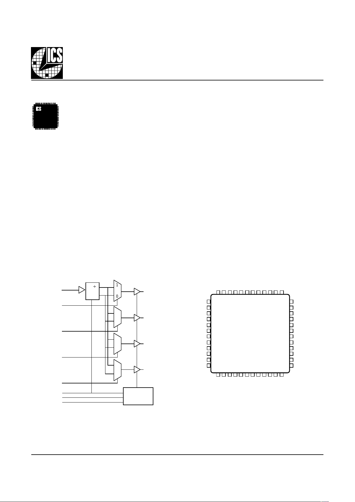
The divide select inputs, DIV_SELx, control the output frequency of each bank. The outputs can be utilized in the ÷1,
÷2 or a combination of ÷1 and ÷2 modes. The bank enable
inputs, BANK_EN0:1, support enabling and disabling each
bank of outputs individually. The master reset input, nMR/
OE, resets the internal frequency dividers and also controls the active and high impedance states of all outputs.
The ICS8701 is characterized at 3.3V and mixed 3.3V input
supply, and 2.5V output supply operating modes. Guaranteed
bank, output and part-to-part skew characteristics make the
ICS8701 ideal for those clock distribution applications demanding well defined performance and repeatability.
FEATURES
• 20 LVCMOS outputs, 7Ω typical output impedance
• 1 L VCMOS clock input
• Maximum output frequency up to 250MHz
• Bank enable logic allows unused banks to be disabled
in reduced fanout applications
• Output skew: 250ps (maximum)
• Part-to-part skew: 600ps (maximum)
• Bank skew: 200ps (maximum)
• Multiple frequency skew: 300ps (maximum)
• 3.3V or mixed 3.3V input, 2.5V output operating
supply modes
• 0°C to 70°C ambient operating temperature
• Other divide values available on request
BLOCK DIAGRAM PIN ASSIGNMENT
DIV_SELA
DIV_SELB
DIV_SELC
DIV_SELD
nMR/OE
BANK_EN0
BANK_EN1
QAO - QA4
QB0 - QB4
QC0 - QC4
QD0 - QD4
CLK
48 47 46 45 44 43 42 41 40 39 38 37
13 14 15 16 17 18 19 20 21 22 23 24
1
2
3
4
5
6
7
8
9
10
11
12
36
35
34
33
32
31
30
29
28
27
26
25
QC3
VDDO
QC4
QD0
VDDO
QD1
GND
QD2
GND
QD3
V
DDO
QD4
QB1
V
DDO
QB0
QA4
VDDO
QA3
GND
QA2
GND
QA1
V
DDO
QA0
DIV_SELA
DIV_SELB
CLK
GND
VDDBANK_EN0
GND
BANK_EN1
VDDnMR/OE
DIV_SELC
DIV_SELD
GND
QB2
GND
QB3
V
DDO
QB4
QC0
V
DDO
QC1
GND
QC2
GND
48-Pin LQFP
7mm x 7mm x 1.4mm
Y Package
Top View
ICS8701
HiPerClockS™
,&6
1
0
÷1
÷2
1
0
1
0
1
0
Bank Enable
Logic
Page 2
8701CY www.icst.com/products/hiperclocks.html REV. B AUGUST 2, 2001
2
Integrated
Circuit
Systems, Inc.
ICS8701
LOW SKEW ÷1, ÷2
CLOCK GENERA T OR
TABLE 1. PIN DESCRIPTIONS
rebmuNemaNepyTnoitpircseD
,5,2
,62,11
,53,23
44,14
V
ODD
rewoP.V5.2roV3.3ottcennoC.snipylppustuptuO
,81,9,7
,03,82,12
,64,93,73
84
DNGrewoP.dnuorgottcennoC.dnuorgylppusrewoP
02,61V
DD
rewoP.V3.3ottcennoC.snipylppusevitisoP
,72,52
,92
33,13
,1AQ,0AQ
,2AQ
4AQ,3AQ
tuptuO
.slevelecafretniSOMCVL.stuptuoAknaB
7
W
.ecnadepmituptuolacipyt
,63,43
,83
24,04
,1BQ,0BQ
,2BQ
4BQ,3BQ
tuptuO
.slevelecafretniSOMCVL.stuptuoBknaB
7
W
.ecnadepmituptuolacipyt
,54,34
,74
3,1
,1CQ,0CQ
,2CQ
4CQ,3CQ
tuptuO
.slevelecafretniSOMCVL.stuptuoCknaB
7
W
.ecnadepmituptuolacipyt
,6,4
,8
21,01
,1DQ,0DQ
,2DQ
4DQ,3DQ
tuptuO
slevelecafretniSOMCVL.stuptuoDknaB
7
W
.ecnadepmituptuolacipyt
22KLCtupnInwodlluP.tupnikcolcLTTVL/SOMCVL
31DLES_VIDtupnIpulluP
.stuptuoDknabrofnoisividycneuqerfslortnoC
.slevelecafretniSOMCVL
41CLES_VIDtupnIpulluP
.stuptuoCknabrofnoisividycneuqerfslortnoC
.slevelecafretniSOMCVL
32BLES_VIDtupnIpulluP
.stuptuoBknabrofnoisividycneuqerfslortnoC
.slevelecafretniSOMCVL
42ALES_VIDtupnIpulluP
.stuptuoAknabrofnoisividycneuqerfslortnoC
.slevelecafretniSOMCVL
91,71
,1NE_KNAB
0NE_KNAB
tupnIpulluP .slevelecafretniSOMCVL.sknabybstuptuoselbasiddnaselbanE
51EO/RMntupnIpulluP
.stuptuollaselbasiddnaselbanE.elbanetuptuodnateserretsaM
.slevelecafretniSOMCVL
Page 3
8701CY www.icst.com/products/hiperclocks.html REV. B AUGUST 2, 2001
3
Integrated
Circuit
Systems, Inc.
ICS8701
LOW SKEW ÷1, ÷2
CLOCK GENERATOR
TABLE 2. PIN CHARACTERISTICS
TABLE 3. FUNCTION TABLE
lobmySretemaraPsnoitidnoCtseTmuminiMlacipyTmumixaMstinU
C
NI
ecnaticapaCtupnI
KLC 4Fp
,BLES_VID,ALES_VID
,DLES_VID,CLES_VID
,EO/RMN,0NE_KNAB
,1NE_KNAB
4
R
PULLUP
rotsiseRpulluPtupnI 15K
W
R
NWODLLUP
rotsiseRnwodlluPtupnI 15K
W
C
DP
ecnaticapaCnoitapissiDrewoP
)tuptuorep(
V
DD
V,
ODD
V564.3=Fp
V
DD
,V564.3=
V
ODD
V526.2=
Fp
R
TUO
ecnadepmItuptuO 7
W
stupnIstuptuO
EO/RMn1NE_KNAB0NE_KNABxLES_VID4AQ-0AQ4BQ-0BQ4CQ-0CQ4DQ-0DQ
xQ
ycneuqerf
0X XX ZiHZiHZiHZiHorez
10 0 0 evitcAZiHZiHZiH2/NIf
11 00 evitcAevitcAZiHZiH2/NIf
10 10 evitcAevitcAevitcAZiH2/NIf
11 10 evitcAevitcAevitcAevitcA2/NIf
10 0 1 evitcAZiHZiHZiHNIf
11 01 evitcAevitcAZiHZiHNIf
10 1 1 evitcAevitcAevitcAZiHNIf
11 11 evitcAevitcAevitcAevitcANIf
Page 4
8701CY www.icst.com/products/hiperclocks.html REV. B AUGUST 2, 2001
4
Integrated
Circuit
Systems, Inc.
ICS8701
LOW SKEW ÷1, ÷2
CLOCK GENERA T OR
ABSOLUTE MAXIMUM RATINGS
Supply Voltage, V
DDx
4.6V
Inputs, V
I
-0.5V to VDD + 0.5V
Outputs, V
O
-0.5V to V
DDO
+ 0.5V
Package Thermal Impedance, θ
JA
47.9°C/W (0lfpm)
Storage T emperature, T
STG
-65°C to 150°C
Stresses beyond those listed under Absolute Maximum Ratings may cause permanent damage to the device. These ratings
are stress specifications only. Functional operation of product at these conditions or any conditions beyond those
listed in the
DC Characteristics
or
AC Characteristics
is not implied. Exposure to absolute maximum rating conditions for
extended periods may affect product reliability.
TABLE 4A. POWER SUPPLY DC CHARACTERISTICS, V
DD
= V
DDO
= 3.3V±5%, TA =0°C TO 70°C
lobmySretemaraPsnoitidnoCtseTmuminiMlacipyTmumixaMstinU
V
HI
tupnI
egatloVhgiH
,BLES_VID,ALES_VID
,DLES_VID,CLES_VID
,1NE_KNAB,0NE_KNAB
EO/RMn
28.3V
KLC28.3V
V
LI
tupnI
egatloVwoL
,BLES_VID,ALES_VID
,DLES_VID,CLES_VID
,1NE_KNAB,0NE_KNAB
EO/RMn
V
DD
V564.3=3.0-8.0V
KLCV
DD
V564.3=3.0-3.1V
I
HI
tupnI
tnerruChgiH
,BLES_VID,ALES_VID
,DLES_VID,CLES_VID
,1NE_KNAB,0NE_KNAB
EO/RMn
V
DD
=V
NI
V564.3=5Aµ
KLCV
DD
=V
NI
V564.3=051Aµ
I
LI
tupnI
tnerruCwoL
,BLES_VID,ALES_VID
,DLES_VID,CLES_VID
,1NE_KNAB,0NE_KNAB
EO/RMn
V
DD
,V564.3=VNIV0=051-Aµ
KLCV
DD
,V564.3=VNIV0=5-Aµ
V
HO
egatloVhgiHtuptuO
V
DD
V=
ODD
V531.3=
I
HO
Am63-=
6.2V
V
LO
egatloVwoLtuptuO
V
DD
V=
ODD
V531.3=
I
LO
Am63=
5.0V
lobmySretemaraPsnoitidnoCtseTmuminiMlacipyTmumixaMstinU
V
DD
egatloVylppuSevitisoP 531.33.3564.3V
V
ODD
egatloVylppuStuptuO 531.33.3564.3V
I
DD
tnerruCylppuSrewoPtnecseiuQ
V
DD
V=
HI
V564.3=
V
LI
V0=
59Am
TABLE 4B. LVCMOS DC CHARACTERISTICS, V
DD
= V
DDO
= 3.3V±5%, TA =0°C TO 70°C
Page 5
8701CY www.icst.com/products/hiperclocks.html REV. B AUGUST 2, 2001
5
Integrated
Circuit
Systems, Inc.
ICS8701
LOW SKEW ÷1, ÷2
CLOCK GENERATOR
TABLE 5A. AC CHARACTERISTICS, V
DD
= V
DDO
= 3.3V±5%, TA =0°C TO 70°C
lobmySretemaraPsnoitidnoCtseTmuminiMlacipyTmumixaMstinU
f
XAM
ycneuqerFtupnImumixaM 052zHM
t
DP
1ETON;yaleDnoitagaporPZHM0
£f£
zHM0022.24.3sn
t
)b(ks7,2ETON;wekSknaBtaegdegnisirnoderusaeMV
ODD
2/002sp
t
)o(ks7,3ETON;wekStuptuOtaegdegnisirnoderusaeMV
ODD
2/052sp
t
(ksw)
;wekSycneuqerFelpitluM
7,4ETON
taegdegnisirnoderusaeMV
ODD
2/003sp
t
)pp(ks7,5ETON;wekStraP-ot-traPtaegdegnisirnoderusaeMV
ODD
2/006sp
t
R
6ETON;emiTesiRtuptuO%07ot%03082058sp
t
F
6ETON;emiTllaFtuptuO%07ot%03082058sp
cdoelcyCytuDtuptuO
ZHM0
£f£
zHM002
2/ELCYCt
5.0-
2/ELCYCt
2/ELCYCt
5.0+
sn
zHM002=f25.23sn
t
NE
;emiTelbanEtuptuO
6ETON
zHM01=f6sn
t
SID
;emiTelbasiDtuptuO
6ETON
zHM01=f6sn
.esiwrehtodetonsselnuzHM002taderusaemsretemarapllA
.tniopgnissorctuptuoehtottupniehtfotniop%05ehtmorfderusaeM:1ETON
.snoitidnocdaollauqehtiwdnasegatlovylppusemasehttastuptuofoknabanihtiwwekssadenifeD:2ETON
.snoitidnocdaollauqehtiwdnasegatlovylppusemasehttastuptuofosknabssorcawekssadenifeD:3ETON
segatlovylppusemasehthtiwycneuqerftnereffidtagnitarepostuptuofosknabssorcawekssadenifeD:4ETON
.snoitidnocdaollauqedna
dnasegatlovylppusemasehttagnitareposecivedtnereffidnostuptuoneewtebtaweksehtsadenifeD:5ETON
.stniopssorcehttaderusaemerastuptuoeht,ecivedhcaenostupnifoepytemasehtgnisU.snoitidnocdaollauqehtiw
.noitcudorpnidetsettoN.noitaziretcarahcybdeetnaraugerasretemarapesehT:6ETON
.56dradnatSCEDEJhtiwecnadroccanidenifedsiretemarapsihT:7ETON
Page 6

8701CY www.icst.com/products/hiperclocks.html REV. B AUGUST 2, 2001
6
Integrated
Circuit
Systems, Inc.
ICS8701
LOW SKEW ÷1, ÷2
CLOCK GENERA T OR
TABLE 4C. POWER SUPPLY DC CHARACTERISTICS, V
DD
= 3.3V±5%, V
DDO
= 2.5V±5%, TA = 0°C TO 70°C
TABLE 4D. L VCMOS DC CHARACTERISTICS, V
DD
= 3.3V±5%, V
DDO
= 2.5V±5%, TA = 0°C TO 70°C
lobmySretemaraPsnoitidnoCtseTmuminiMlacipyTmumixaMstinU
V
DD
egatloVylppuSevitisoP 531.33.3564.3V
V
ODD
egatloVylppuStuptuO 573.25.2526.2V
I
DD
tnerruCylppuSrewoPtnecseiuQ
V
DD
V=
HI
V564.3=
V
LI
V0=
59Am
lobmySretemaraPsnoitidnoCtseTmuminiMlacipyTmumixaMstinU
V
HI
tupnI
egatloVhgiH
,BLES_VID,ALES_VID
,DLES_VID,CLES_VID
,1NE_KNAB,0NE_KNAB
EO/RMn
28.3V
KLC28.3V
V
LI
tupnI
egatloVwoL
,BLES_VID,ALES_VID
,DLES_VID,CLES_VID
,1NE_KNAB,0NE_KNAB
EO/RMn
V
DD
V564.3=3.0-8.0V
KLCV
DD
V564.3=3.0-3.1V
I
HI
tupnI
tnerruChgiH
,BLES_VID,ALES_VID
,DLES_VID,CLES_VID
,1NE_KNAB,0NE_KNAB
EO/RMn
V
DD
=V
NI
V564.3=5Aµ
KLCV
DD
=V
NI
V564.3=051Aµ
I
LI
tupnI
tnerruCwoL
,BLES_VID,ALES_VID
,DLES_VID,CLES_VID
,1NE_KNAB,0NE_KNAB
EO/RMn
V
DD
,V564.3=VNIV0=051-Aµ
KLCV
DD
,V564.3=VNIV0=5-Aµ
V
HO
egatloVhgiHtuptuO
V
DD
,V531.3=
V
ODD
573.2=
I
HO
Am72-=
8.1V
V
LO
egatloVwoLtuptuO
V
DD
,V531.3=
V
ODD
573.2=
I
LO
Am72=
5.0V
Page 7

8701CY www.icst.com/products/hiperclocks.html REV. B AUGUST 2, 2001
7
Integrated
Circuit
Systems, Inc.
ICS8701
LOW SKEW ÷1, ÷2
CLOCK GENERATOR
TABLE 5B. AC CHARACTERISTICS, V
DD
= 3.3V±5%, V
DDO
= 2.5V±5%, TA = 0°C TO 70°C
lobmySretemaraPsnoitidnoCtseTmuminiMlacipyTmumixaMstinU
f
XAM
ycneuqerFtupnImumixaM 052zHM
t
DP
1ETON;yaleDnoitagaporPZHM0
£f£
zHM0026.26.3sn
t
)b(ks7,2ETON;wekSknaBtaegdegnisirnoderusaeMV
ODD
2/522sp
t
)o(ks7,3ETON;wekStuptuOtaegdegnisirnoderusaeMV
ODD
2/052sp
t
(ksw)
;wekSycneuqerFelpitluM
7,4ETON
taegdegnisirnoderusaeMV
ODD
2/003sp
t
)pp(ks7,5ETON;wekStraP-ot-traPtaegdegnisirnoderusaeMV
ODD
2/006sp
t
R
6ETON;emiTesiRtuptuO%07ot%03082058sp
t
F
6ETON;emiTllaFtuptuO%07ot%03082058sp
cdoelcyCytuDtuptuO
ZHM0
£f£
zHM002
2/ELCYCt
5.0-
2/ELCYCt
2/ELCYCt
5.0+
sn
zHM002=f25.23sn
t
NE
;emiTelbanEtuptuO
6ETON
zHM01=f6sn
t
SID
;emiTelbasiDtuptuO
6ETON
zHM01=f6sn
.esiwrehtodetonsselnuzHM002taderusaemsretemarapllA
.tniopgnissorctuptuoehtottupniehtfotniop%05ehtmorfderusaeM:1ETON
.snoitidnocdaollauqehtiwdnasegatlovylppusemasehttastuptuofoknabanihtiwwekssadenifeD:2ETON
.snoitidnocdaollauqehtiwdnasegatlovylppusemasehttastuptuofosknabssorcawekssadenifeD:3ETON
segatlovylppusemasehthtiwycneuqerftnereffidtagnitarepostuptuofosknabssorcawekssadenifeD:4ETON
.snoitidnocdaollauqedna
dnasegatlovylppusemasehttagnitareposecivedtnereffidnostuptuoneewtebtaweksehtsadenifeD:5ETON
.stniopssorcehttaderusaemerastuptuoeht,ecivedhcaenostupnifoepytemasehtgnisU.snoitidnocdaollauqehtiw
.noitcudorpnidetsettoN.noitaziretcarahcybdeetnaraugerasretemarapesehT:6ETON
.56dradnatSCEDEJhtiwecnadroccanidenifedsiretemarapsihT:7ETON
Page 8

8701CY www.icst.com/products/hiperclocks.html REV. B AUGUST 2, 2001
8
Integrated
Circuit
Systems, Inc.
ICS8701
LOW SKEW ÷1, ÷2
CLOCK GENERA T OR
PARAMETER MEASUREMENT INFORMATION
FIGURE 1A - 3.3V OUTPUT LOAD TEST CIRCUIT
SCOPE
Qx
LVCMOS
VDD = +1.65V
V
DDO
= 1.65V
V
DD
GND = -1.65V
V
DDO
FIGURE 1B - 2.5V OUTPUT LOAD TEST CIRCUIT
SCOPE
Qx
LVCMOS
V
DDO
= +1.25V
V
DDO
GND = -1.25V
Page 9

8701CY www.icst.com/products/hiperclocks.html REV. B AUGUST 2, 2001
9
Integrated
Circuit
Systems, Inc.
ICS8701
LOW SKEW ÷1, ÷2
CLOCK GENERATOR
FIGURE 2 - OUTPUT SKEW
tsk(o)
Qx
Qy
FIGURE 3 - PART-TO-PART SKEW
Qx
Qy
P ART 1
P ART 2
tsk(pp)
Page 10

8701CY www.icst.com/products/hiperclocks.html REV. B AUGUST 2, 2001
10
Integrated
Circuit
Systems, Inc.
ICS8701
LOW SKEW ÷1, ÷2
CLOCK GENERA T OR
FIGURE 4 - INPUT AND OUTPUT RISE AND FALL TIME
Clock Inputs
and Outputs
20%
80%
20%
80%
t
R
t
F
V
SWING
FIGURE 5 - PROPAGATION DELAY
t
PD
VCC/2
CLK
QAx, QBx,
QCx, QDx
FIGURE 6 - odc & t
PERIOD
Pulse Width
t
PERIOD
t
PW
t
PERIOD
odc =
CLK, QAx, QBx,
QCx, QDx
Page 11

8701CY www.icst.com/products/hiperclocks.html REV. B AUGUST 2, 2001
11
Integrated
Circuit
Systems, Inc.
ICS8701
LOW SKEW ÷1, ÷2
CLOCK GENERATOR
POWER CONSIDERATIONS
This section provides information on power dissipation and junction temperature for the ICS8701-01.
Equations and example calculations are also provided.
1. Power Dissipation.
The total power dissipation for the ICS8701-01 is the sum of the core power plus the power dissipated in the load(s).
The following is the power dissipation for V
DD
= 3.3V + 5% = 3.465V , which gives worst case results.
NOTE: Please refer to Section 3 for details on calculating power dissipated in the load.
• Power (core)
MAX
= V
DD_MAX
* I
DD_MAX
= 3.465V * 95mA = 329.2mW
• Power (outputs)
MAX
= 32mW/Loaded Output pair
If all outputs are loaded, the total power is 20 * 32mW = 640mW
T otal Power
_MAX
(3.465V , with all outputs switching) = 329.2mW + 640mW = 969.2mW
2. Junction T emperature.
Junction temperature, Tj, is the temperature at the junction of the bond wire and bond pad and directly affects the reliability of the
device. The maximum recommended junction temperature for HiPerClockS
TM
devices is 125°C.
The equation for Tj is as follows: Tj = θ
JA
* Pd_total + T
A
Tj = Junction T emperature
θ
JA
= junction-to-ambient thermal resistance
Pd_total = T otal device power dissipation (example calculation is in section 1 above)
T
A
= Ambient T emperature
In order to calculate junction temperature, the appropriate junction-to-ambient thermal resistance θ
JA
must be used . Assuming a
moderate air flow of 200 linear feet per minute and a multi-layer board, the appropriate value is 42.1°C/W per T able 6 below .
Therefore, Tj for an ambient temperature of 70°C with all outputs switching is:
70°C + 0.969W * 42.1°C/W = 110.8°C. This is well below the limit of 125°C
This calculation is only an example. Tj will obviously vary depending on the number of loaded outputs, supply voltage, air flow,
and the type of board (single layer or multi-layer).
θθ
θθ
θJA by Velocity (Linear Feet per Minute)
0 200 500
Single-Layer PCB, JEDEC Standard Test Boards 67.8°C/W 55.9°C/W 50.1°C/W
Multi-Layer PCB, JEDEC Standard Test Boards 47.9°C/W 42.1°C/W 39.4°C/W
NOTE: Most modern PCB designs use multi-layered boards. The data in the second row pertains to most designs.
Table 6. Thermal Resistance
θθ
θθ
θJA for 48-pin LQFP, Forced Convection
Page 12

8701CY www.icst.com/products/hiperclocks.html REV. B AUGUST 2, 2001
12
Integrated
Circuit
Systems, Inc.
ICS8701
LOW SKEW ÷1, ÷2
CLOCK GENERA T OR
3. Calculations and Equations.
The purpose of this section is to derive the power dissipated into the load.
L VCMOS output driver circuit and termination are shown in
Figure 7.
To calculate worst case power dissipation into the load, use the following equations which assume a 50Ω load, and a termination
voltage of VDD- 2V .
Pd_H is power dissipation when the output drives high.
Pd_L is the power dissipation when the output drives low .
Pd_H = (V
OH_MAX /RL
) * (V
DD_MAX
- V
OH_MAX
)
Pd_L = (V
OL_MAX /RL
) * (V
DD_MAX
- V
OL_MAX
)
• For logic high, V
OUT
= V
OH_MAX
= V
DD_MAX
– 1.2V
• For logic low, V
OUT
= V
OL_MAX
= V
DD_MAX
– 0.4V
Pd_H = (1.2V/50Ω) * (2V - 1.2V) = 19.2mW
Pd_L = (0.4V/50Ω) * (2V - 0.4V) = 12.8mW
T otal Power Dissipation per output pair = Pd_H + Pd_L = 32mW
FIGURE 7 - LVCMOS DRIVER CIRCUIT AND TERMINATION
V
DDO
V
OUT
RL
50
Ω
Q1
Page 13

8701CY www.icst.com/products/hiperclocks.html REV. B AUGUST 2, 2001
13
Integrated
Circuit
Systems, Inc.
ICS8701
LOW SKEW ÷1, ÷2
CLOCK GENERATOR
RELIABILITY INFORMATION
TRANSISTOR COUNT
The transistor count for ICS8701 is: 1743
TABLE 7. θ
JA
VS
. AIR FLOW TABLE
θθ
θθ
θJA by Velocity (Linear Feet per Minute)
0 200 500
Single-Layer PCB, JEDEC Standard Test Boards 67.8°C/W 55.9°C/W 50.1°C/W
Multi-Layer PCB, JEDEC Standard Test Boards 47.9°C/W 42.1°C/W 39.4°C/W
NOTE: Most modern PCB designs use multi-layered boards. The data in the second row pertains to most designs.
Page 14

8701CY www.icst.com/products/hiperclocks.html REV. B AUGUST 2, 2001
14
Integrated
Circuit
Systems, Inc.
ICS8701
LOW SKEW ÷1, ÷2
CLOCK GENERA T OR
NOITAIRAVCEDEJ
SRETEMILLIMNISNOISNEMIDLLA
LOBMYS
CBB
MUMINIMLANIMONMUMIXAM
N
84
A
----06.1
1A
50.0--51.0
2A
53.104.154.1
b
71.022.072.0
c
90.0--02.0
D
CISAB00.9
1D
CISAB00.7
2D
.feR05.5
E
CISAB00.9
1E
CISAB00.7
2E
.feR05.5
e
CISAB05.0
L
54.006.057.0
q
0
°
--
7
°
ccc
----80.0
PACKAGE OUTLINE - Y SUFFIX
TABLE 8. PACKAGE DIMENSIONS
Reference Document: JEDEC Publication 95, MS-026
Page 15

8701CY www.icst.com/products/hiperclocks.html REV. B AUGUST 2, 2001
15
Integrated
Circuit
Systems, Inc.
ICS8701
LOW SKEW ÷1, ÷2
CLOCK GENERATOR
TABLE 9. ORDERING INFORMATION
rebmuNredrO/traPgnikraMegakcaPtnuoCerutarepmeT
YC1078SCIYC1078SCIPFQLdaeL84yartrep052C°07otC°0
TYC1078SCIYC1078SCIleeRdnaepaTnoPFQLdaeL840001C°07otC°0
While the information presented herein has been checked for both accuracy and reliability, Integrated Circuit Systems, Incorporated (ICS) assumes no responsibility for either its use
or for infringement of any patents or other rights of third parties, which would result from its use. No other circuits, patents, or licenses are implied. This product is intended for use
in normal commercial applications. Any other applications such as those requiring extended temperature range, high reliability, or other extraordinary environmental requirements are
not recommended without additional processing by ICS. ICS reserves the right to change any circuitry or specifications without notice. ICS does not authorize or warrant any ICS
product for use in life support devices or critical medical instruments.
 Loading...