

Page 1
Integrated
Circuit
Systems, Inc.
ICS8701-01
L
OW SKEW ¸1, ¸2 CLOCK
GENERAT OR W/POLARITY CONTROL
GENERAL DESCRIPTION
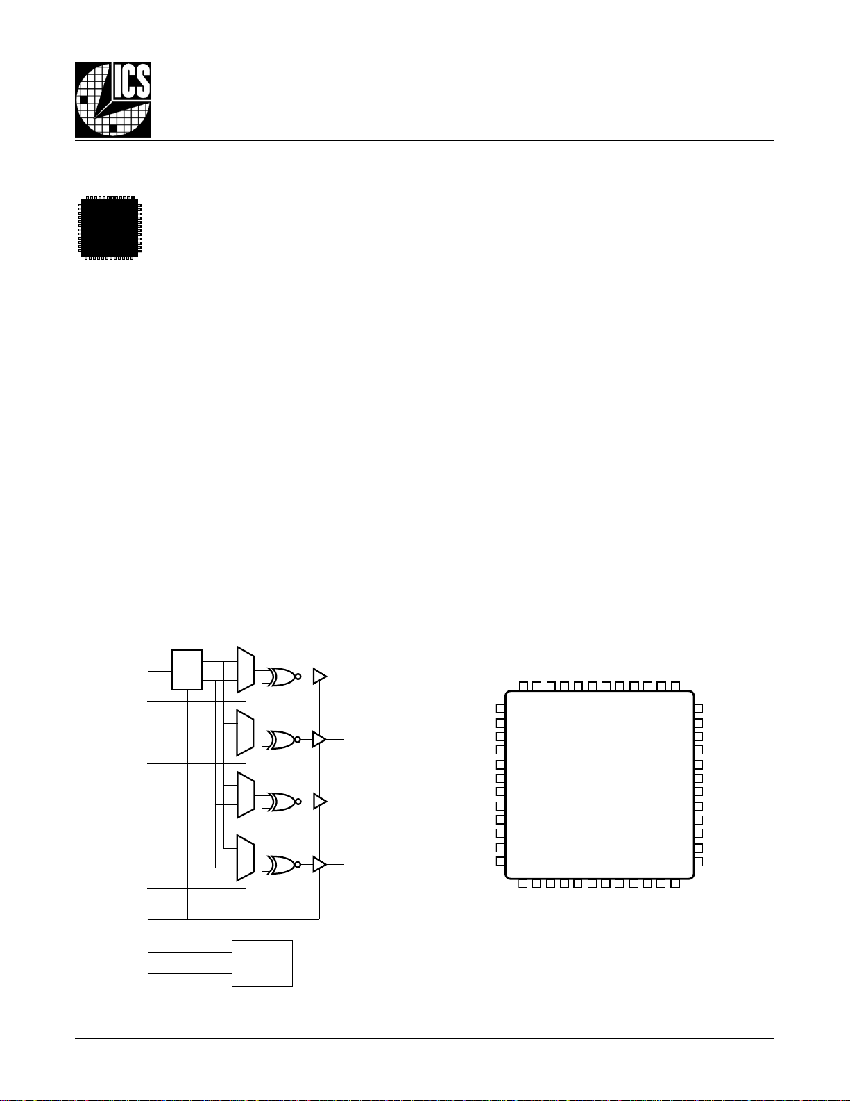
The ICS8701-01 is a low skew, ÷1, ÷2 Clock
,&6
HiPerClockS™
minated transmission lines. The effective fanout can be increased from 20 to 40 by utilizing the ability of the outputs to
drive two series terminated lines.
The divide select inputs, DIV_SELx, control the output frequency of each bank. The outputs can be utilized in the ÷1,
÷2 or a combination of ÷1 and ÷2 modes. The master reset/
output enable input, nMR/OE, resets the internal dividers and
controls the active and high impedance states of all outputs.
The output polarity inputs, INV0:1, control the polarity (inverting or non-inverting) of the outputs of each bank. Outputs
QA0-QA4 are inverting for every combination of the INV0:1
input. The timing relationship between the inverting and noninverting outputs at different frequencies is shown in the Timing Diagrams.
The ICS8701-01 is characterized at 3.3V and mixed 3.3V input supply, and 2.5V output supply operating modes. Guaranteed bank, output and part-to-part skew characteristics
make the ICS8701-01 ideal for those clock distribution applications demanding well defined performance and repeatability.
Generator and a member of the HiPerClockS
fa mil y of Hi gh Performance Clock Solutions
from ICS. The low impedance LVCMOS outputs
are designed to drive 50Ω series or parallel ter-
FE ATURES
20 LVCMOS outputs, 7Ω typical output impedance
Output frequency up to 250 MHz
250ps bank skew, 300ps output skew, 350ps multiple
frequency skew, 700ps part-to-part skew
Selectable inverting and non-inverting outputs
LVCMOS / LVTTL clock input
LVCMOS / LVTTL control inputs
Bank enable logic allows unused banks to be disabled
in reduced fanout applications
3.3V or mixed 3.3V input, 2.5V output operating
supply modes
48 lead low-profile QFP (LQFP), 7mm x 7mm x 1.4mm
package body, 0.5mm package lead pitch
0°C to 70°C ambient operating temperature
Other divide values available on request
BLOCK DIAGRAM PIN ASSIGNMENT
GND
LVCMOS_CLK
DIV_SELA
DIV_SELB
DIV_SELC
DIV_SELD
nMR/OE
INV0
INV1
÷1
÷2
1
0
1
0
1
0
1
0
Output
Polarity
Control
QAO - QA4
QB0 - QB4
QC0 - QC4
QD0 - QD4
QC3
VDDOC
QC4
QD0
VDDOD
QD1
GND
QD2
GND
QD3
VDDOD
QD4
GND
48 47 46 45 44 43 42 41 40 39 38 37
1
2
3
4
5
6
7
8
9
10
11
12
13 14 15 16 17 18 19 20 21 22 23 24
DIV_SELD
QC1
QC2
ICS8701-01
VDDI
nMR/OE
DIV_SELC
48-Pin LQFP
VDDOC
INV1
QC0
GND
QB4
INV0
VDDOB
VDDI
Y Package
Top View
GND
QB2
QB3
DIV_SELB
LVCMOS_CLK
GND
GND
36
35
34
33
32
31
30
29
28
27
26
25
DIV_SELA
QB1
VDDOB
QB0
QA4
VDDOA
QA3
GND
QA2
GND
QA1
VDDOA
QA0
8701-01 www.icst.com REV. A - AUGUST 28, 2000
1
Page 2
Integrated
Circuit
Systems, Inc.
TABLE 1. PIN DESCRIPTIONS
rebmuNemaNepyTnoitpircseD
44,2CODDVrewoP .V5.2roV3.3ottcennoC.ylppusrewopCknaBtuptuO
11,5DODDVrewoP .V5.2roV3.3ottcennoC.ylppusrewopDknaBtuptuO
23,62AODDVrewoP .V5.2roV3.3ottcennoC.ylppusrewopCknaBtuptuO
14,53BODDVrewoP .V5.2roV3.3ottcennoC.ylppusrewopBknaBtuptuO
,81,9,7
,03,82,12
,64,93,73
84
02,61IDDVrewoP.V3.3ottcennoC.ylppusrewoptupnI
,92,72,52
33,13
,83,63,43
24,04
,74,54,34
3,1
,8,6,4
21,01
22KLC_SOMCVLtupnIpulluP.slevelecafretniSOMCVL.tupnikcolC
31DLES_VIDtupnIpulluP .slevelecafretniSOMCVL.stuptuoDknabrofnoisividycneuqerfslortnoC
41CLES_VIDtupnIpulluP .slevelecafretniSOMCVL.stuptuoCknabrofnoisividycneuqerfslortnoC
32BLES_VIDtupnIpulluP .slevelecafretniSOMCVL.stuptuoBknabrofnoisividycneuqerfslortnoC
42ALES_VIDtupnIpulluP .slevelecafretniSOMCVL.stuptuoAknabrofnoisividycneuqerfslortnoC
91,710VNI,1VNItupnIpulluP .slevelecafretniSOMCVL.sknabybstuptuofoytiralopsenimreteD
51EO/RMntupnIpulluP
DNGrewoP.dnuorgottcennoC.dnuorG
,2AQ,1AQ,0AQ
4AQ,3AQ
,2BQ,1BQ,0BQ
4BQ,3BQ
,2CQ,1CQ,0CQ
4CQ,3CQ
,2DQ,1DQ,0DQ
4DQ,3DQ
tuptuO7.slevelecafretniSOMCVL.stuptuoAknaB Ω .ecnadepmituptuolacipyt
tuptuO7.slevelecafretniSOMCVL.stuptuoBknaB Ω .ecnadepmituptuolacipyt
tuptuO7.slevelecafretniSOMCVL.stuptuoCknaB Ω .ecnadepmituptuolacipyt
tuptuO7.slevelecafretniSOMCVL.stuptuoDknaB Ω .ecnadepmituptuolacipyt
ICS8701-01
L
OW SKEW ¸1, ¸2 CLOCK
GENERAT O R W/POLARITY CONTROL
steS.WOLotstuptuognitrevni-nonsteseR.elbanetuptuodnateserretsaM
.slevel
ecafretniSOMCVL.stuptuollaselbasiddnaselbanE.HGIHotstuptuognitrevni
TABLE 2. PIN CHARACTERISTICS
lobmySretemaraPsnoitidnoCtseTmuminiMlacipyTmumixaMstinU
NICecnaticapaCtupnI Fp
PULLUPRrotsiseRpulluPtupnI 15KΩ
DPCecnaticapaCnoitapissiDrewoP
)tuptuorep(
TUORecnadepmItuptuO 7
V564.3=xODDV,IDDV Fp
V526.2=xODDV,V564.3=IDDV Fp
TABLE 3. FUNCTION TABLE
stupnI stuptuO
EO/RMnxLES_VID1VNI0VNIAKNABBKNABCKNABDKNABycneuqerfxQ
0XX X ZiHZiHZiHZiHorez
10 0 0 gnitrevnIgnitrevni-noNgnitrevni-noNgnitrevni-noN2/NIf
10 0 1 gnitrevnIgnitrevnIgnitrevni-noNgnitrevni-noN2/NIf
10 1 0 gnitrevnIgnitrevnIgnitrevnIgnitrevni-noN2/NIf
10 1 1 gnitrevnIgnitrevnIgnitrevnIgnitrevnI2/NIf
110 0 gnitrevnIgnitrevni-noNgnitrevni-noNgnitrevni-noNNIf
110 1 gnitrevnIgnitrevnIgnitrevni-noNgnitrevni-noNNIf
111 0 gnitrevnIgnitrevnIgnitrevnIgnitrevni-noNNIf
111 1 gnitrevnIgnitrevnIgnitrevnIgnitrevnINIf
Ω
8701-01 www.icst.com REV. A - AUGUST 28, 2000
2
Page 3
Integrated
Circuit
L
OW SKEW ¸1, ¸2 CLOCK
ICS8701-01
Systems, Inc.
GENERAT OR W/POLARITY CONTROL
ABSOLUTE MAXIMUM RATINGS
Supply Voltage 4.6V
Inputs -0.5V to VDDI + 0.5V
Outputs -0.5V to VDDOx + 0.5V
Ambient Operating Temperature 0°C to 70°C
Storage Temperature -65°C to 150°C
Stresses beyond those listed under Absolute Maximum Ratings may cause permanent damage to the device. These ratings are stress
specifications only and functional operation of product at these condition or any conditions beyond those listed in the DC Electrical
Characteristics or AC Electrical Characteristics is not implied. Exposure to absolute maximum rating conditions for extended periods may
affect product reliability.
TABLE 4A. DC ELECTRICAL CHARACTERISTICS, VDDI = VDDOX = 3.3V±5%, TA = 0°C TO 70°C
lobmySretemaraP snoitidnoCtseTmuminiMlacipyTmumixaMstinU
IDDVegatloVylppuSrewoPtupnI 531.33.3564.3V
xODDVegatloVylppuSrewoPtuptuO 531.33.3564.3V
HIVegatloVhgiHtupnI
LIVegatloVwoLtupnI
HIItnerruChgiHtupnI V564.3=NIV=IDDV5Aµ
LIItnerruCwoLtupnI V0=NIV=IDDV051-Aµ
DDItnerruCylppuSrewoPtnecseiuQ 07Am
HOVegatloVhgiHtuptuO
LOVegatloVwoLtuptuO
KLC_SOMCVL2567.3V
KLC_SOMCVL3.0-3.1V
KLC_SOMCVLtpecxellA
KLC_SOMCVLtpecxellA
V564.3=IDDV
V531.3=IDDV
V531.3=xODDV
Am63-=HOI
V531.3=xODDV
Am63=LOI
2567.3V
3.0-8.0V
6.2V
5.0V
TABLE 5A. AC ELECTRICAL CHARACTERISTICS, VDDI = VDDOX = 3.3V±5%, TA=0°C TO 70°C
lobmySretemaraPsnoitidnoCtseTmuminiMlacipyTmumixaMstinU
XAMfycneuqerFtupnImumixaM 052zHM
HLpthgiH-ot-woL,yaleDnoitagaporPZHM0 < f ≤ zHM0025.25.3sn
LHptwoL-ot-hgiH,yaleDnoitagaporPZHM0 < f ≤ zHM0025.25.3sn
)b(kst2ETON;wekSknaB 2/xODDVtaegdegnillafnoderusaeM052sp
)o(kst3ETON;wekStuptuO 2/xODDVtaegdegnillafnoderusaeM003sp
(kst ω)4ETON;wekSycneuqerFelpitluM 2/xODDVtaegdegnillafnoderusaeM053sp
)pp(kst5ETON;wekStraPottraP 2/xODDVtaegdegnillafnoderusaeM007sp
Rt6ETON;emiTesiRtuptuO 051007sp
Ft6ETON;emiTllaFtuptuO 051007sp
05htiwdetanimretstuptuollA.esiwrehtodetonsselnuzHM002taderusaemsretemarapllA:1ETON Ω .2/xODDVot
2/ELCYCt
5.0-
2/ELCYCt
.snoitidnocdaollauqehtiwdnasegatlovylppusemasehttastuptuofoknabanihtiwwekssadenifeD:2ETON
WPthtdiWesluPtuptuO
NEtemiTelbanEtuptuO6ETON; 6sn
SIDtemiTelbasiDtuptuO6ETON; 6sn
.snoitidnoc
.snoitidnocdaollauqednasegatlov
.snoitidnocdaollauqehtiwdna
ZHM0 < f < zHM002
zHM002=f25.23sn
.noitcudorpnidetsettoN.noitaziretcarahcybdeetnaraugerasretemarapesehT:6ETON
2/ELCYCt
5.0+
daollauqehtiwdnasegatlovylppusemasehttanoitceridemasehtnignihctiwsstuptuofosknabssorcawekssadenifeD:3ETON
sn
ylppusemasehthtiwseicneuqerftnereffidtagnitareponoitceridemasehtnignihctiwsstuptuofosknabssorcawekssadenifeD:4ETON
segatlovylppusemasehttagnitareposecivedtnereffidnonoitceridemasehtnignihctiwsstuptuotnereffidtaweksehtsadenifeD:5ETON
8701-01 www.icst.com REV. A - AUGUST 28, 2000
3
Page 4

Integrated
Circuit
L
OW SKEW ¸1, ¸2 CLOCK
ICS8701-01
Systems, Inc.
GENERAT O R W/POLARITY CONTROL
TABLE 4B. DC ELECTRICAL CHARACTERISTICS, VDDI = 3.3V±5%, VDDOX = 2.5V±5%, TA = 0°C TO 70°C
lobmySretemaraPsnoitidnoCtseTmuminiMlacipyTmumixaMstinU
IDDVegatloVylppuSrewoPtupnI 531.33.3564.3V
xODDVegatloVylppuSrewoPtuptuO 573.25.2526.2V
HIVegatloVhgiHtupnI
LIVegatloVwoLtupnI
HIItnerruChgiHtupnI V564.3=NIV=IDDV5Aµ
LIItnerruCwoLtupnI V0=NIV=IDDV051-Aµ
DDItnerruCylppuSrewoPtnecseiuQ 07Am
HOVegatloVhgiHtuptuO
LOVegatloVwoLtuptuO
KLC_SOMCVL2567.3V
KLC_SOMCVL3.0-3.1V
KLC_SOMCVLtpecxellA
KLC_SOMCVLtpecxellA
V564.3=IDDV
V531.3=IDDV
V531.3=IDDV
V573.2=xODDV
Am72-=HOI
V531.3=IDDV
V573.2=xODDV
Am72=LOI
2567.3V
3.0-8.0V
8.1V
5.0V
TABLE 5B. AC ELECTRICAL CHARACTERISTICS, VD DI = 3.3V±5%, VDDO = 2.5V±5%, T A = 0°C TO 70°C
lobmySretemaraPsnoitidnoCtseTmuminiMlacipyTmumixaMstinU
XAMfycneuqerFtupnImumixaM 052zHM
HLpthgiH-ot-woL,yaleDnoitagaporPZHM0 < f ≤ zHM0025.25.3sn
LHptwoL-ot-hgiH,yaleDnoitagaporPZHM0 < f ≤ zHM0025.25.3sn
)b(kst2ETON;wekSknaB 2/xODDVtaegdegnillafnoderusaeM003sp
)o(kst3ETON;wekStuptuO 2/xODDVtaegdegnillafnoderusaeM003sp
(kst ω)4ETON;wekSycneuqerFelpitluM 2/xODDVtaegdegnillafnoderusaeM053sp
)pp(kst5ETON;wekStraPottraP 2/xODDVtaegdegnillafnoderusaeM007sp
Rt6ETON;emiTesiRtuptuO 051027sp
Ft6ETON;emiTllaFtuptuO 051027sp
05htiwdetanimretstuptuollA.esiwrehtodetonsselnuzHM002taderusaemsretemarapllA:1ETON Ω .2/xODDVot
2/ELCYCt
5.0-
2/ELCYCt
.snoitidnocdaollauqehtiwdnasegatlovylppusemasehttastuptuofoknabanihtiwwekssadenifeD:2ETON
WPthtdiWesluPtuptuO
NEtemiTelbanEtuptuO6ETON; 6sn
SIDtemiTelbasiDtuptuO6ETON; 6sn
.snoitidnoc
stuptuofosknabssorcawekssadenifeD:4ETON onoitceridemasehtnignihctiws ylppusemasehthtiwycneuqerftnereffidtagnitarep
.snoitidnocdaollauqednasegatlov
stuptuotnereffidtaweksehtsadenifeD:5ETON noitceridemasehtnignihctiws segatlovylppusemasehttagnitareposecivedtnereffidno
.snoitidnocdaollauqehtiwdna
ZHM0 < f < zHM002
zHM002=f25.23sn
.noitcudorpnidetsettoN.noitaziretcarahcybdeetnaraugerasretemarapesehT:6ETON
2/ELCYCt
5.0+
daollauqehtiwdnasegatlovylppusemasehttanoitceridemasehtnignihctiwsstuptuofosknabssorcawekssadenifeD:3ETON
sn
8701-01 www.icst.com REV. A - AUGUST 28, 2000
4
Page 5

Integrated
Circuit
Systems, Inc.
FIGURE 1A, 1B - TIMING DIAGRAMS
LVCMOS_CLK
QA, ÷1, INV
QB, ÷2, INV
QC, ÷2, NINV
QD, ÷1, NINV
L
OW SKEW ¸1, ¸2 CLOCK
GENERAT OR W/POLARITY CONTROL
FIGURE 1A - ACTIVE, ÷1, ÷2, INVERTING AND NON-INVERTING
ICS8701-01
nMR/OE
LVCMOS_CLK
QA, ÷1, INV
QB, ÷2, INV
QC, ÷2, NINV
QD, ÷1, NINV
High Impedance Active
FIGURE 1B - RESET TO ACTIVE, ÷1, ÷2, INVERTING AND NON-INVERTING
8701-01 www.icst.com REV. A - AUGUST 28, 2000
5
Page 6

Integrated
Circuit
Systems, Inc.
FIGURE 2A, 2B - TIMING WAVEFORMS
ICS8701-01
L
OW SKEW ¸1, ¸2 CLOCK
GENERAT O R W/POLARITY CONTROL
CLK
nMR/OE
3.3V
VDDI/2
0V
tPHL
Q
VDDI/2
VDDI/2
tPLH
VDDI/2
FIGURE 2A - P ROPAGATION DELAYS
fin = 200MHz, Vamp = 3.3V, tr = tf = 600ps
3.3V
VDDI/2
0V
tPHZ
Q
VOH
VOH - 300mV
VDDI/2
tPZH
VDDO/2
Q
tPLZ
VDDO/2
VOL + 300mV
VOL
tPZL
FIGURE 2B - DISABLE AND ENABLE TIMES
fin = 10MHz, Vamp = 3.3V, tr = tf = 600ps
8701-01 www.icst.com REV. A - AUGUST 28, 2000
6
Page 7

Integrated
Circuit
L
OW SKEW ¸1, ¸2 CLOCK
ICS8701-01
Systems, Inc.
GENERAT OR W/POLARITY CONTROL
FIGURE 3A, 3B- SKEW DEFINITIONS & WAVEFORMS
Bank Skew - Skew within a bank of outputs at the same supply voltages and with equal load conditions.
CLK
VDDO/2 VDDO/2
Qx0
○○○○○○○○
tsk(b) tsk(b)
VDDO/2 VDDO/2
Qx4
FIGURE 3A - BANK SKEW
fin = 200MHz, Vamp = 3.3V, tr = tf = 200ps
Output Skew - Skew across banks of outputs switching in the same direction at the same supply voltages and with equal load
conditions.
CLK
VDDO/2
QA0 - QA4
tsk(o)
VDDO/2
tsk(o)
VDDO/2
QB0 - QB4
QC0 - QC4
QD0 - QD4
8701-01 www.icst.com REV. A - AUGUST 28, 2000
FIGURE 3B - INVERTING OUTPUT SKEW
fin = 200MHz, Vamp = 3.3V, tr = tf = 200ps
7
VDDO/2
Page 8

Integrated
Circuit
L
OW SKEW ¸1, ¸2 CLOCK
ICS8701-01
Systems, Inc.
GENERAT O R W/POLARITY CONTROL
FIGURE 3C, 3D- SKEW DEFINITIONS & WAVEFORMS
Multiple Frequency Skew - Skew across banks of outputs switching in the same direction operating at different frequencies with
the same supply voltages and equal load conditions.
CLK
QA0 - QA4,
QB0 - QB4,
QC0 - QC4,
or
QD0 - QD4
in ÷1, inverting
QA0 - QA4,
QB0 - QB4,
QC0 - QC4,
or
QD0 - QD4
in ÷2, inverting
VDDO/2
tsk(w)
VDDO/2
FIGURE 3C - MULTIPLE FREQUENCY SKEW
fin = 200MHz, Vamp = 3.3V, tr = tf = 200ps
Part to Part Skew - Skew at different outputs switching in the same direction on different devices operating at the same supply
voltages and with equal load conditions.
CLK
PART 1 QA0 - QA4
QB0 - QB4
QC0 - QC4
QD0 - QD4
inverting
PART 2 QA0 - QA4
QB0 - QB4
QC0 - QC4
QD0 - QD4
inverting
VDDO/2 VDDO/2
tsk(p) tsk(p)
VDDO/2 VDDO/2
FIGURE 3B - OUTPUT SKEW
fin = 200MHz, Vamp = 3.3V, tr = tf = 200ps
8701-01 www.icst.com REV. A - AUGUST 28, 2000
8
Page 9

Integrated
Circuit
Systems, Inc.
PACKAGE OUTLINE AND DIMENSIONS - Y S UFFIX
NOTE 4
NOTE 4
D
D
NOTE 5, 7
NOTE 5, 7
D1
D1
NOTE 3
NOTE 3
-D-
-D-
NOTE 3
NOTE 3
-A-
-A-
e
e
N/4 TIPS
N/4 TIPS
0.20 C A-B D4X
0.20 C A-B D4X 0.20 C A-B D0.20 C A-B D4X
SEE DETAIL “A”
SEE DETAIL “A”
8 PLACES
8 PLACES
11 / 13°
11 / 13°
D/2
D/2
D1/2
D1/2
NOTE 3
NOTE 3
-B-
-B-
E/2
E/2
E1/2
E1/2
A
A
NOTE 2 / / 0.10 C
NOTE 2 / / 0.10 C
-H-
-H-
ccc
ccc
-C-
-C-
SEE DETAIL “B”
SEE DETAIL “B”
ICS8701-01
L
OW SKEW ¸1, ¸2 CLOCK
GENERAT OR W/POLARITY CONTROL
-A, B, OR -D-
-A, B, OR -D-
b
b
E
E1
E
E1
N
N
N
N
O
O
O
O
T
T
T
T
E
E
E
E
4
4
5,
5,
7
7
NOTES:
1. ALL DIME NSIONS AND TOLERA NCING CONFORM TO ANSI
Y14.5-1982
2. DATUM PLANE -H- LOCATED AT MOLD PARTING LINE AND
COINCIDENT WITH LEAD, WHERE LEAD EXITS PLASTIC BODY
AT BOTTOM OF PARTING LINE.
3. DATUMS A-B AND -D- TO BE DETE RMINED AT CENTERLINE
BETWEEN LEADS WHERE LEADS EXIT PLASTIC AT DATUM
PLANE -H- .
4. TO BE DETERMINED AT SEATING PLACE -C- .
5. DIM ENSIONS D1 AND E1 DO NOT INCLUDE MOLD
PROT RUSION.
6. “N” IS THE TOTAL NUMBER OF TERMINALS.
7. THESE DIME NSIONS TO BE DETEREMINED AT DATUM PLANE
-H-.
8. PACKAGE TOP DIMENSIONS ARE SMALLER THAN BOTTOM
DIM ENSIONS AND TOP OF PACKAGE WILL NOT OVE R HANG
BOTTOM OF PACKAGE.
9. DIM ENSION b DOES NOT INCLUDE DAMBAR PROTRUSION.
ALLOWABLE DAMBAR PROTRUSION SHALL BE 0.08mm TOTAL
IN EXCESS OF THE b DIMENSION AT MAXIMUM MATERIAL
CONDITION.
10. CO NTROLLING DIM ENSION: MILLIMET ER.
11. THIS OUTLINE CONFORM S TO JEDEC PUBL IBCATION 95
REGISTRATION M S-026, VA RIAT ION BBC.
12. A1 IS DEFINED AS THE DISTANCE FROM THE SEATING PLANE
TO THE LOWEST POINT OF THE PACKAGE.
-A, B, OR -D-
-A, B, OR -D-
e / 2
e / 2
b
b
b
b
1
1
0.08
0.08
R. MIN.
R. MIN.
0.20 MIN.
0.20 MIN.
1.00 REF.
1.00 REF.
ddd M C A-B S D S
WITH LEAD FINISH
WITH LEAD FINISH
BASE METAL
BASE METAL
0° MIN.
0° MIN.
0° -7 °
0° -7 °
L
L
0.08/0.20 R.
0.08/0.20 R.
0.25
0.25
GAUGE PLANE
GAUGE PLANE
S
b1
b1
ccc
ccc
ddd
ddd
S
Y
Y
M
M
B
B
O
O
L
L
A
A
A
A
1
1
A
A
2
2
D
D
D
D
1
1
E
E
E
E
1
1
L
L
N
N
e
e
b
b
JEDEC VARI ATIO N
JEDEC VARI ATIO N
ALL DIM E NSIONS IN MI LLIM E TERS
ALL DIM E NSIONS IN MI LLIM E TERS
MIN. NOM. MAX.
MIN. NOM. MAX.
0.05 0.15
0.05 0.15
1.35 1.40 1.45
1.35 1.40 1.45
9.00 BSC.
9.00 BSC.
7.00 BSC.
7.00 BSC.
9.00 BSC.
9.00 BSC.
7.00 BSC.
7.00 BSC.
0.45 0.60 0.75
0.45 0.60 0.75
0.17 0.22 0.27
0.17 0.22 0.27
0.17 0.20 0.23
0.17 0.20 0.23
BBC
BBC
48
48
0.5 BSC.
0.5 BSC.
1.60
1.60
0.08
0.08
0.08
0.08
12
12
7, 8
7, 8
7, 8
7, 8
N
N
O
O
T
T
E
E
4
4
4
4
9
9
NOTE 9 ddd M C A-B S D S
NOTE 9
0.09 / 0.20 0.09 / 0.16
0.09 / 0.20 0.09 / 0.16
-0.05 S
-0.05 S
-0.05 S
DATUM
DATUM
A2
A2
PLANE
PLANE
-H-
-H-
A1
A1
8701-01 www.icst.com REV. A - AUGUST 28, 2000
9
Page 10

Integrated
Circuit
Systems, Inc.
ORDERING INFORMATION
Y10-1078SCI10-1078SCIPFQLdaeL84yartrep052C°07otC°0
TY10-1078SCI10-1078SCIleeRdnaepaTnoPFQLdaeL840002C°07otC°0
ICS8701-01
L
OW SKEW ¸1, ¸2 CLOCK
GENERAT O R W/POLARITY CONTROL
rebmuNredrO/traPgnikraMegakcaPtnuoCerutarepmeT
While the information presented herein has been checked for both accuracy and reliability, Integrated Circuit Systems, Incorporated (ICS) assumes no responsibility for either its use or
for infringement of any patents or other rights of third parties, which would result from its use. No other circuits, patents, or licenses are implied. This product is intended for use in normal
commercial applications. Any other applications such as those requiring extended temperature range, high reliability, or other extraordinary environmental requirements are not recommended without additional processing by ICS. ICS reserves the right to change any circuitry or specifications without notice. ICS does not authorize or warrant any ICS product for use
in life support devices or critical medical instruments.
8701-01 www.icst.com REV. A - AUGUST 28, 2000
10
 Loading...