

Page 1
Integrated
Circuit
Systems, Inc.
ICS8523
LOW SKEW, 1-TO-4
DIFFERENTIAL-TO-L VHSTL FANOUT BUFFER
GENERAL DESCRIPTION
,&6
HiPerClockS™
CLK, nCLK pair can accept most standard differential input
levels. The PCLK, nPCLK pair can accept L VPECL, CML, or
SSTL input levels. The clock enable is internally synchronized
to eliminate runt pulses on the outputs during asynchronous
assertion/deassertion of the clock enable pin.
Guaranteed output and part-to-part skew characteristics
make the ICS8523 ideal for those applications demanding
well defined performance and repeatability.
The ICS8523 is a low skew, high performance 1-to-4 Differential-to-L VHSTL fanout buffer
and a member of the HiPerClockS™ family of High
Performance Clock Solutions from ICS. The
ICS8523 has two selectable clock inputs. The
FEATURES
• 4 differential 1.8V L VHSTL outputs
• Selectable CLK, nCLK or L VPECL clock inputs
• CLK, nCLK pair can accept the following differential input
levels: L VDS, L VPECL, L VHSTL, SSTL, HCSL
• PCLK, nPCLK supports the following input types:
L VPECL, CML, SSTL
• Maximum output frequency up to 650MHz
• Translates any single-ended input signal to 1.8V L VHSTL
levels with resistor bias on nCLK input
• Output skew: 30ps (maximum)
• Part-to-part skew: 150ps (maximum)
• Propagation delay: 1.6ns (maximum)
• 3.3V core, 1.8V output operating supply
• 0°C to 70°C ambient operating temperature
• Industrial temperature information available upon request
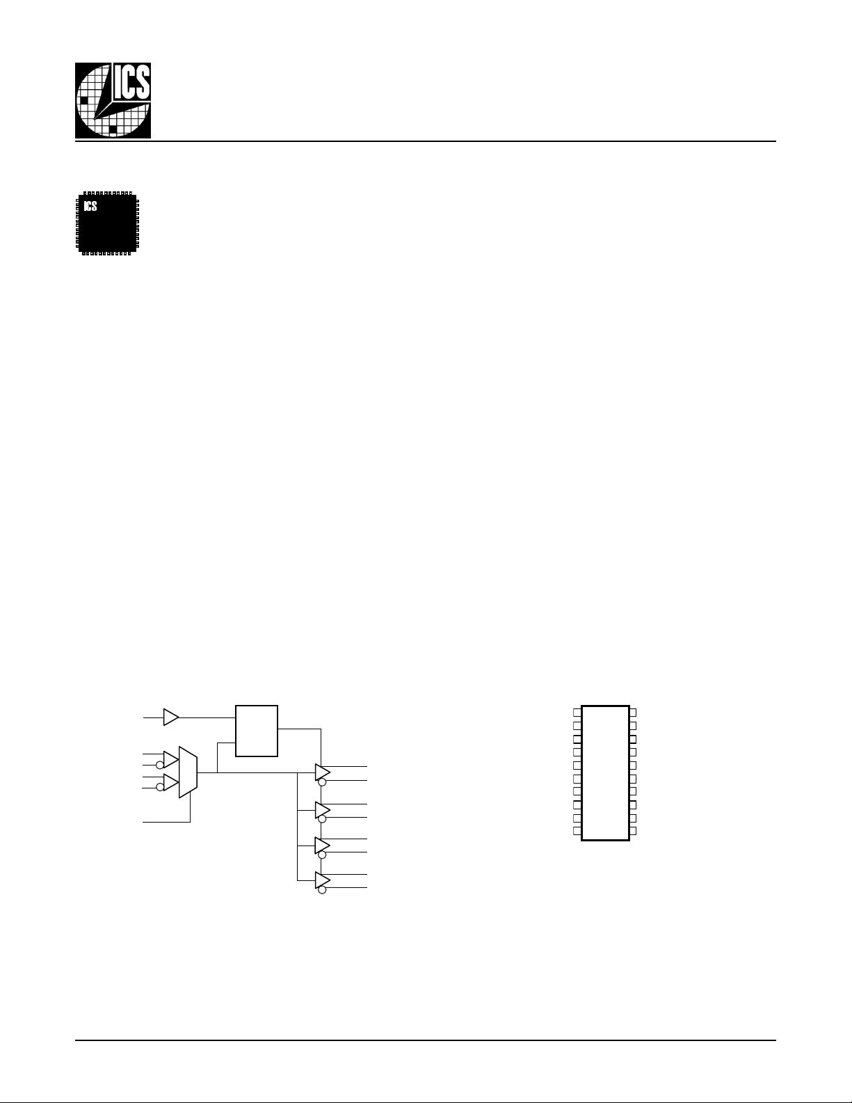
BLOCK DIAGRAM PIN ASSIGNMENT
20
1
CLK_EN
CLK
nCLK
PCLK
nPCLK
CLK_SEL
D
Q
LE
0
1
Q0
nQ0
Q1
nQ1
Q2
nQ2
Q3
nQ3
6.5mm x 4.4mm x 0.92mm body package
GND
CLK_EN
CLK_SEL
CLK
nCLK
PCLK
nPCLK
nc
nc
V
DD
20-Lead TSSOP
2
3
4
5
6
7
8
9
10
ICS8523
G Package
Top View
8523BG www.icst.com/products/hiperclocks.html REV. B JULY 31, 2001
1
19
18
17
16
15
14
13
12
11
Q0
nQ0
V
DDO
Q1
nQ1
Q2
nQ2
V
DDO
Q3
nQ3
Page 2
Integrated
Circuit
Systems, Inc.
TABLE 1. PIN DESCRIPTIONS
rebmuNemaNepyTnoitpircseD
1DNGrewoP.dnuorgottcennoC.dnuorgylppusrewoP
2NE_KLCtupnIpulluP
3LES_KLCtupnInwodlluP
4KLCtupnInwodlluP.tupnikcolclaitnereffidgnitrevni-noN
5KLCntupnIpulluP.tupnikcolclaitnereffidgnitrevnI
6KLCPtupnInwodlluP.tupnikcolcLCEPVLlaitnereffidgnitrevni-noN
7KLCPntupnIpulluP.tupnikcolcLCEPVLlaitnereffidgnitrevnI
9,8cndesunU.tcennocoN
01V
21,113Q,3QntuptuO.slevelecafretniLTSHVL.riaptuptuolaitnereffiD
81,31V
51,412Q,2QntuptuO.slevelecafretniLTSHVL.riaptuptuolaitnereffiD
71,611Q,1QntuptuO.slevelecafretniLTSHVL.riaptuptuolaitnereffiD
02,910Q,0QntuptuO.slevelecafretniLTSHVL.riaptuptuolaitnereffiD
pulluP
:ETON
DD
ODD
dna
nwodlluP
rewoP.V3.3ottcennoC.nipylppusevitisoP
rewoP.V8.1ottcennoC.snipylppustuptuO
ICS8523
LOW SKEW, 1-TO-4
DIFFERENTIAL-TO-LVHSTL FANOUT BUFFER
kcolcwollofstuptuokcolc,HGIHnehW.elbanekcolcgnizinorhcnyS
decroferastuptuoQn,woldecroferastuptuoQ,WOLnehW.tupni
.slevelecafretniLTTVL/SOMCVL.hgih
KLCPn,KLCPlaitnereffidstceles,HGIHnehW.tupnitceleskcolC
.stupniKLCn,KLCstceles,WOLnehW.stupni
.slevelecafretniLTTVL/SOMCVL
.seulavlacipytrof,scitsiretcarahCniP,2elbaTeeS.srotsisertupnilanretniotsrefer
TABLE 2. PIN CHARACTERISTICS
lobmySretemaraPsnoitidnoCtseTmuminiMlacipyTmumixaMstinU
C
NI
R
PULLUP
R
NWODLLUP
KLCn,KLC4Fp
ecnaticapaCtupnI
rotsiseRpulluPtupnI 15KΩ
rotsiseRnwodlluPtupnI 15KΩ
KLCPn,KLCP4Fp
LES_KLC,NE_KLC4Fp
8523BG www.icst.com/products/hiperclocks.html REV. B JULY 31, 2001
2
Page 3
Integrated
Circuit
Systems, Inc.
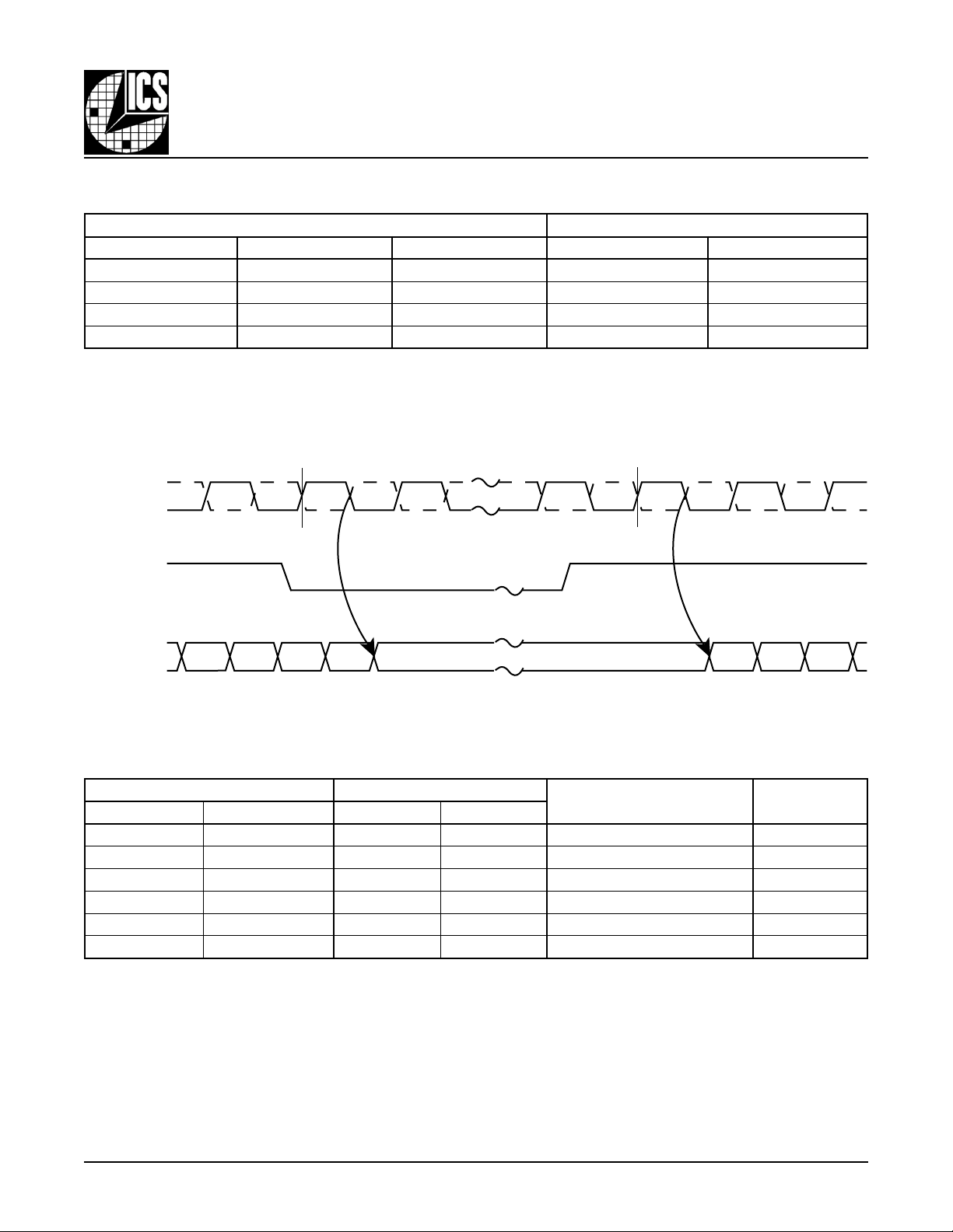
TABLE 3A. CONTROL INPUT FUNCTION TABLE
stupnIstuptuO
NE_KLCLES_KLCecruoSdetceleS3Qurht0Q3Qnurht0Qn
00 KLCn,KLCWOL;delbasiDHGIH;delbasiD
01 KLCPn,KLCPWOL;delbasiDHGIH;delbasiD
10 KLCn,KLCdelbanEdelbanE
11 KLCPn,KLCPdelbanEdelbanE
.1erugiFninwohssa
.B3elbaTni
ICS8523
LOW SKEW, 1-TO-4
DIFFERENTIAL-TO-L VHSTL FANOUT BUFFER
egdekcolctupnignillafdnagnisiragniwollofdelbanerodelbasiderastuptuokcolceht,sehctiwsNE_KLCretfA
debircsedsastupniKLCPn,KLCPdnaKLCn,KLCehtfonoitcnufaerastuptuoehtfoetatseht,edomevitcaehtnI
nCLK, nPCLK
Disabled
CLK, PCLK
CLK_EN
nQ0 - nQ3
Q0 - Q3
TABLE 3B. CLOCK INPUT FUNCTION TABLE
stupnIstuptuO
KLCProKLCKLCPnroKLCn3Qurht0Q3Qnurht0Qn
00WOLHGIHlaitnereffiDotlaitnereffiDgnitrevnInoN
11 HGIHWOLlaitnereffiDotlaitnereffiDgnitrevnInoN
01ETON;desaiBWOLHGIHlaitnereffiDotdednEelgniSgnitrevnInoN
11ETON;desaiBHGIHWOLlaitnereffiDotdednEelgniSgnitrevnInoN
1ETON;desaiB0HGIHWOLlaitnereffiDotdednEelgniSgnitrevnI
1ETON;desaiB1WOLHGIHlaitnereffiDotdednEelgniSgnitrevnI
.sleveldedneelgnistpeccaottupni
Enabled
FIGURE 1 - CLK_EN TIMING DIAGRAM
edoMtuptuOottupnIytiraloP
laitnereffidehtgniriwsessucsidhcihw,9erugiF,8egapnonoitcesnoitamrofnInoitacilppAehtotreferesaelP:1ETON
8523BG www.icst.com/products/hiperclocks.html REV. B JULY 31, 2001
3
Page 4
Integrated
Circuit
Systems, Inc.
LOW SKEW, 1-TO-4
ICS8523
DIFFERENTIAL-TO-LVHSTL FANOUT BUFFER
ABSOLUTE MAXIMUM RATINGS
Supply Voltage, V
Inputs, V
I
Outputs, V
Package Thermal Impedance, θ
Storage T emperature, T
DDx
O
JA
STG
Stresses beyond those listed under Absolute Maximum Ratings may cause permanent damage to the device. These ratings
are stress specifications only . Functional operation of product at these conditions or any conditions beyond those listed in the
DC Characteristics
or
AC Characteristics
ods may affect product reliability .
4.6V
-0.5V to VDD + 0.5V
-0.5V to V
DDO
+ 0.5V
73.2°C/W
-65°C to 150°C
is not implied. Exposure to absolute maximum rating conditions for extended peri-
TABLE 4A. POWER SUPPLY DC CHARACTERISTICS, V
= 3.3V±5%, V
DD
lobmySretemaraPsnoitidnoCtseTmuminiMlacipyTmumixaMstinU
V
DD
V
ODD
I
DD
egatloVylppuSrewoPtupnI 531.33.3564.3V
egatloVylppuSrewoPtuptuO6.18.10.2V
tnerruCylppuSrewoP 05Am
TABLE 4B. LVCMOS / LVTTL DC CHARACTERISTICS, V
lobmySretemaraPsnoitidnoCtseTmuminiMlacipyTmumixaMstinU
V
HI
V
LI
I
HI
I
LI
TABLE 4C. DIFFERENTIAL DC CHARACTERISTICS, V
lobmySretemaraPsnoitidnoCtseTmuminiMlacipyTmumixaMstinU
I
HI
I
LI
V
PP
V
RMC
2,1ETON
egatloVhgiHtupnILES_KLC,NE_KLC2567.3V
egatloVwoLtupnILES_KLC,NE_KLC3.0-8.0V
tnerruChgiHtupnI
tnerruCwoLtupnI
tnerruChgiHtupnI
tnerruCwoLtupnI
NE_KLCV
LES_KLCV
NE_KLCV
LES_KLCV
= 3.3V±5%, V
DD
KLCnV
KLCV
KLCnV
KLCV
DD
DD
egatloVtupnIkaeP-ot-kaeP 51.03.1V
;egatloVtupnIedoMnommoC
.
VsadenifedsiegatlovedomnommoC:2ETON
= 3.3V±5%, V
DD
DD
DD
DD
DD
V=
DD
NI
V=
DD
NI
= 1.8V±0.2V , TA = 0°C TO 70°C
DDO
= 1.8V±0.2V, TA = 0°C TO 70°C
DDO
V=
NI
V=
NI
DDO
V564.3=5Aµ
V564.3=051Aµ
V,V564.3=
V0=051-Aµ
NI
V,V564.3=
V0=5-Aµ
NI
= 1.8V±0.2V , TA = 0°C TO 70°C
V564.3=5Aµ
V564.3=051Aµ
V,V564.3=
V0=051-Aµ
NI
V,V564.3=
V0=5-Aµ
NI
5.0V
VsiKLCndnaKLCrofegatlovtupnimumixamehtsnoitacilppadedneelgnisroF:1ETON
DD
.V3.0+
58.0-V
DD
8523BG www.icst.com/products/hiperclocks.html REV. B JULY 31, 2001
4
Page 5

Integrated
Circuit
Systems, Inc.
ICS8523
LOW SKEW, 1-TO-4
DIFFERENTIAL-TO-L VHSTL FANOUT BUFFER
TABLE 4D. LVPECL DC CHARACTERISTICS, V
lobmySretemaraPsnoitidnoCtseTmuminiMlacipyTmumixaMstinU
I
HI
I
LI
V
PP
V
RMC
tnerruChgiHtupnI
tnerruCwoLtupnI
KLCPV
KLCPnV
KLCPV
KLCPnV
egatloVtupnIkaeP-ot-kaeP 3.01V
TABLE 4D. LVHSTL DC CHARACTERISTICS, V
lobmySretemaraPsnoitidnoCtseTmuminiMlacipyTmumixaMstinU
V
HO
V
LO
V
XO
V
GNIWS
1ETON
1ETON
kaeP-ot-kaeP
;egatloVhgiHtuptuO
;egatloVwoLtuptuO
egatloVrevossorCtuptuO(x%04VHO-VLO+)V
gniwSegatloVtuptuO
05htiwdetanimretstuptuO:1ETON Ω .dnuorgot
= 3.3V±5%, V
DD
2,1ETON;egatloVtupnIedoMnommoC 5.1V
.
VsadenifedsiegatlovedomnommoC:1ETON
HI
= 3.3V±5%, V
DD
= 1.8V±0.2V , TA = 0°C TO 70°C
DDO
V=
DD
NI
V=
DD
NI
DD
DD
= 1.8V±0.2V , TA = 0°C TO 70°C
DDO
V564.3=051Aµ
V564.3=5Aµ
V,V564.3=
V0=5-Aµ
NI
V,V564.3=
V0=051-Aµ
NI
DD
VsiKLCPndnaKLCProfegatlovtupnimumixamehtsnoitacilppadedneelgnisroF:2ETON
.V3.0+
14.1V
04.0V
V(x%06
V-
LO
HO
V+)
LO
LO
57.052.1V
V
V
TABLE 5. AC CHARACTERISTICS, V
= 3.3V±5%, V
DD
= 1.8V±0.2V, TA = 0°C TO 70°C
DDO
lobmySretemaraPsnoitidnoCtseTmuminiMlacipyTmumixaMstinU
f
XAM
t
DP
t
)o(ks4,2ETON;wekStuptuO 03sp
t
)pp(ks4,3ETON;wekStraP-ot-traP 051sp
t
R
t
F
emiTesiRtuptuOzHM05@%08ot%02003007sp
emiTllaFtuptuOzHM05@%08ot%02003007sp
ycneuqerFtuptuOmumixaM 056zHM
1ETON;yaleDnoitagaporP IJ zHM0563.16.1sn
cdoelcyCytuDtuptuO5455%
.esiwrehtodetonsselnuzHM005taderusaemsretemarapllA
.rettijddatonseodtrapehT.tuptuoehtnorettijehtlauqelliwtupniehtnorettijelcycotelcycehT
.tniopgnissorctuptuolaitnereffidehtottniopgnissorctupnilaitnereffidehtmorfderusaeM:1ETON
.snoitidnocdaollauqehtiwdnaegatlovylppusemasehttastuptuoneewtebwekssadenifeD:2ETON
.stniopssorclaitnereffidtuptuotaderusaeM
segatlovylppusemasehttagnitareposecivedtnereffidnostuptuoneewtebwekssadenifeD:3ETON
derusaemerastuptuoeht,ecivedhcaenostupnifoepytemasehtgnisU.snoitidnocdaollauqehtiwdna
.stniopssorclaitnereffidehtta
.56dradnatSCEDEJhtiwecnadroccanidenifedsiretemarapsihT:4ETON
8523BG www.icst.com/products/hiperclocks.html REV. B JULY 31, 2001
5
Page 6

Integrated
Circuit
Systems, Inc.
LOW SKEW, 1-TO-4
ICS8523
DIFFERENTIAL-TO-LVHSTL FANOUT BUFFER
PARAMETER MEASUREMENT INFORMATION
V
DDO
V
DD
SCOPE
Qx
LVHSTL
V
= 3.3V ± 5%
DD
V
= 1.8V ± 0.2V
DDO
nQx
GND = 0V
nCLK, nPCLK
Qx
nQx
Qy
V
CLK, PCLK
GND
FIGURE 2 - OUTPUT LOAD TEST CIRCUIT
DD
VPP
Cross Points
FIGURE 3 - DIFFERENTIAL INPUT LEVEL
V
CMR
nQy
tsk(o)
FIGURE 4 - OUTPUT SKEW
8523BG www.icst.com/products/hiperclocks.html REV. B JULY 31, 2001
6
Page 7

Integrated
Circuit
Systems, Inc.
Qx
PART 1
nQx
Qy
PART 2
nQy
ICS8523
LOW SKEW, 1-TO-4
DIFFERENTIAL-TO-L VHSTL FANOUT BUFFER
tsk(pp)
FIGURE 5 - PART-TO-PART SKEW
Clock Inputs
and Outputs
CLK, PCLK
nCLK, nPCLK
Q0 - Q3
nQ0 - nQ3
80%
20%
t
R
t
F
FIGURE 6 - INPUT AND OUTPUT RISE AND FALL TIME
t
PD
FIGURE 7 - PROPAGATION DELAY
80%
20%
V
SWING
CLK, PCLK, Qx
nCLK, nPCLK, nQx
Pulse Width
t
PERIOD
t
odc =
8523BG www.icst.com/products/hiperclocks.html REV. B JULY 31, 2001
PW
t
PERIOD
FIGURE 8 - odc & t
7
PERIOD
Page 8

Integrated
Circuit
Systems, Inc.
LOW SKEW, 1-TO-4
DIFFERENTIAL-TO-LVHSTL FANOUT BUFFER
APPLICATION INFORMATION
WIRING THE DIFFERENTIAL INPUT TO ACCEPT SINGLE ENDED LEVELS
ICS8523
Figure 9
generated by the bias resistors R1, R2 and C1. This bias circuit should be located as close as possible to the input pin. The ratio of
R1 and R2 might need to be adjusted to position the V_REF in the center of the input voltage swing. For example, if the input clock
swing is only 2.5V and V
shows how the differential input can be wired to accept single ended levels. The reference voltage V_REF ~ VDD/2 is
= 3.3V , V_REF should be 1.25V and R2/R1 = 0.609.
DD
CLK_IN
C1
0.1uF
FIGURE 9: SINGLE ENDED SIGNAL DRIVING DIFFERENTIAL INPUT
R1
1K
V_REF
R2
1K
VDD
+
-
8523BG www.icst.com/products/hiperclocks.html REV. B JULY 31, 2001
8
Page 9

Integrated
Circuit
Systems, Inc.
LOW SKEW, 1-TO-4
DIFFERENTIAL-TO-L VHSTL FANOUT BUFFER
POWER CONSIDERATIONS
This section provides information on power dissipation and junction temperature for the ICS8523.
Equations and example calculations are also provided.
1. Power Dissipation.
The total power dissipation for the ICS8523 is the sum of the core power plus the power dissipated in the load(s).
The following is the power dissipation for V
NOTE: Please refer to Section 3 for details on calculating power dissipated in the load.
= 3.3V + 5% = 3.465V , which gives worst case results.
DD
ICS8523
• Power (core)
• Power (outputs)
If all outputs are loaded, the total power is 4 * 32mW = 128mW
Total Power
MAX
_MAX
= V
MAX
* I
DD_MAX
= 32mW/Loaded Output pair
= 3.465V * 50mA = 173.3mW
DD_MAX
(3.465V, with all outputs switching) = 173.3mW + 128mW = 301.3mW
2. Junction T emperature.
Junction temperature, Tj, is the temperature at the junction of the bond wire and bond pad and directly affects the reliability of the
device. The maximum recommended junction temperature for HiPerClockS
The equation for Tj is as follows: Tj = θ
Tj = Junction T emperature
θ
= junction-to-ambient thermal resistance
JA
Pd_total = T otal device power dissipation (example calculation is in section 1 above)
T
= Ambient T emperature
A
In order to calculate junction temperature, the appropriate junction-to-ambient thermal resistance θ
moderate air flow of 200 linear feet per minute and a multi-layer board, the appropriate value is 66.6°C/W per T able 6 below .
Therefore, Tj for an ambient temperature of 70°C with all outputs switching is:
70°C + 0.301W * 66.6°C/W = 90.05°C. This is well below the limit of 125°C
This calculation is only an example. Tj will obviously vary depending on the number of loaded outputs, supply voltage, air flow,
and the type of board (single layer or multi-layer).
* Pd_total + T
JA
A
TM
devices is 125°C.
must be used . Assuming a
JA
T able 6. Thermal Resistance qJA for 20-pin TSSOP, Forced Convection
q
by V elocity (Linear Feet per Minute)
JA
0 200 500
Single-Layer PCB, JEDEC Standard Test Boards 114.5°C/W 98.0°C/W 88.0°C/W
Multi-Layer PCB, JEDEC Standard Test Boards 73.2°C/W 66.6°C/W 63.5°C/W
NOTE: Most modern PCB designs use multi-layered boards. The data in the second row pertains to most designs.
8523BG www.icst.com/products/hiperclocks.html REV. B JULY 31, 2001
9
Page 10

Integrated
Circuit
Systems, Inc.
DIFFERENTIAL-TO-LVHSTL FANOUT BUFFER
3. Calculations and Equations.
The purpose of this section is to derive the power dissipated into the load.
ICS8523
LOW SKEW, 1-TO-4
L VHSTL output driver circuit and termination are shown in
V
DD
Figure 10.
Q1
V
OUT
RL
Ω
50
FIGURE 10 - LVHSTL DRIVER CIRCUIT AND TERMINATION
To calculate worst case power dissipation into the load, use the following equations which assume a 50Ω load, and a termination
voltage of V
Pd_H is power dissipation when the output drives high.
Pd_L is the power dissipation when the output drives low .
DD
- 2V .
Pd_H = (V
Pd_L = (V
OH_MAX /RL
OL_MAX /RL
• For logic high, V
• For logic low, V
) * (V
) * (V
DD_MAX
DD_MAX
= V
OUT
= V
OUT
- V
- V
OH_MAX
OL_MAX
OH_MAX
OL_MAX
= V
)
)
= V
DD_MAX
DD_MAX
– 1.2V
– 0.4V
Pd_H = (1.2V/50Ω) * (2V - 1.2V) = 19.2mW
Pd_L = (0.4V/50Ω) * (2V - 0.4V) = 12.8mW
T otal Power Dissipation per output pair = Pd_H + Pd_L = 32mW
8523BG www.icst.com/products/hiperclocks.html REV. B JULY 31, 2001
10
Page 11

Integrated
Circuit
Systems, Inc.
ICS8523
LOW SKEW, 1-TO-4
DIFFERENTIAL-TO-L VHSTL FANOUT BUFFER
RELIABILITY INFORMATION
TABLE 7. θ
TRANSISTOR COUNT
The transistor count for ICS8523 is: 472
VS
. AIR FLOW TABLE
JA
q
by V elocity (Linear Feet per Minute)
JA
0 200 500
Single-Layer PCB, JEDEC Standard Test Boards 114.5°C/W 98.0°C/W 88.0°C/W
Multi-Layer PCB, JEDEC Standard Test Boards 73.2°C/W 66.6°C/W 63.5°C/W
NOTE: Most modern PCB designs use multi-layered boards. The data in the second row pertains to most designs.
8523BG www.icst.com/products/hiperclocks.html REV. B JULY 31, 2001
11
Page 12

Integrated
Circuit
Systems, Inc.
PACKAGE OUTLINE - G SUFFIX
ICS8523
LOW SKEW, 1-TO-4
DIFFERENTIAL-TO-LVHSTL FANOUT BUFFER
TABLE 8. PACKAGE DIMENSIONS
LOBMYS
N02
A--02.1
1A50.051.0
2A08.050.1
b91.003.0
c90.002.0
D04.606.6
ECISAB04.6
1E03.405.4
eCISAB56.0
L54.057.0
α
aaa--01.0
Reference Document: JEDEC Publication 95, MS-153
8523BG www.icst.com/products/hiperclocks.html REV. B JULY 31, 2001
NIMXAM
°0 °8
12
sretemilliM
Page 13

Integrated
Circuit
Systems, Inc.
TABLE 9. ORDERING INFORMATION
rebmuNredrO/traPgnikraMegakcaPtnuoCerutarepmeT
GB3258SCIGB3258SCIPOSSTdael02ebutrep27C°07otC°0
TGB3258SCIGB3258SCIleeRdnaepaTnoPOSSTdael020052C°07otC°0
ICS8523
LOW SKEW, 1-TO-4
DIFFERENTIAL-TO-L VHSTL FANOUT BUFFER
While the information presented herein has been checked for both accuracy and reliability, Integrated Circuit Systems, Incorporated (ICS) assumes no responsibility for either its use or for infringement
of any patents or other rights of third parties, which would result from its use. No other circuits, patents, or licenses are implied. This product is intended for use in normal commercial applications.
Any other applications such as those requiring extended temperature range, high reliability, or other extraordinary environmental requirements are not recommended without additional processing by
ICS. ICS reserves the right to change any circuitry or specifications without notice. ICS does not authorize or warrant any ICS product for use in life support devices or critical medical instruments.
8523BG www.icst.com/products/hiperclocks.html REV. B JULY 31, 2001
13
 Loading...