

Page 1
PRELIMINARY
Integrated
Circuit
Systems, Inc.
DIFFERENTIAL-TO-3.3V LVHSTL FANOUT BUFFER
GENERAL DESCRIPTION
,&6
HiPerClockS™
pair can accept most standard differential input levels.
Guaranteed output skew, part-to-part skew and crossover
voltage characteristics make the ICS8520 ideal for interfacing to today’s most advanced microprocessor and static
RAMs.
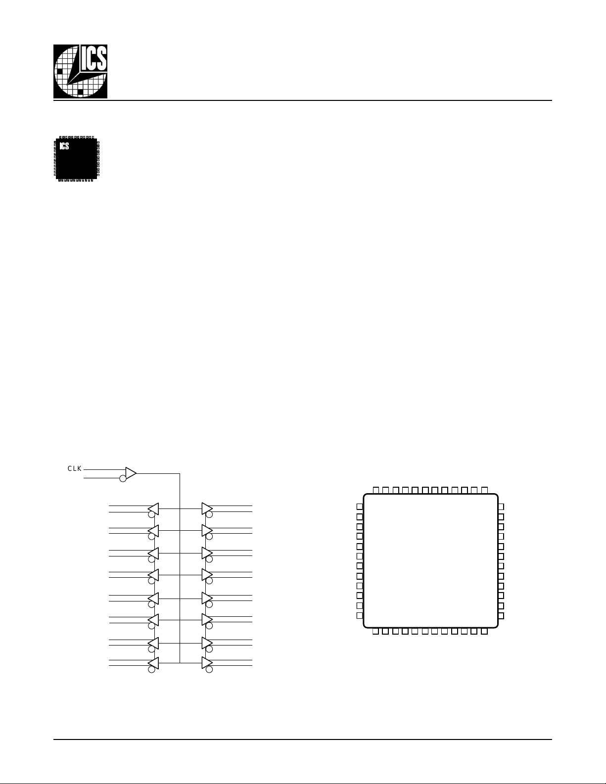
The ICS8520 is a low skew, high performance
1-to-16 Differential-to-3.3V L VHSTL Fanout Buf fer
and a member of the HiPerClockS™ family of
High Performance Clock Solutions from ICS. The
ICS8520 has 1 clock input pair . The CLK, nCLK
ICS8520
LOW SKEW, 1-TO-16
FEATURES
• 16 differential 3.3V L VHSTL outputs each with the ability to
drive 50Ω to ground
• 1 differential CLK, nCLK input pair
• CLK, nCLK pair can accept the following differential input
levels: L VDS, L VPECL, L VHSTL, SSTL, HCSL
• Maximum output frequency up to 500MHz
• Translates single ended input levels to L VHSTL levels with
resistor bias nCLK input
• Output skew: 50ps (maximum)
• Part-to-part skew: 250ps (maximum)
• Propagation delay: 1.6ns (maximum)
• VOH: 1.2V (maximum)
• 40% of VOH ≤ Vcrossover ≤ 60% of VOH
• 3.3V core, 1.8V output operating supply voltages
• 0°C to 70°C ambient operating temperature
BLOCK DIAGRAM PIN ASSIGNMENT
CLK
nCLK
Q0
nQ0
Q1
nQ1
Q2
nQ2
Q3
nQ3
Q4
nQ4
Q5
nQ5
Q6
nQ6
Q7
nQ7
Q15
nQ15
Q14
nQ14
Q13
nQ13
Q12
nQ12
Q11
nQ11
Q10
nQ10
Q9
nQ9
Q8
nQ8
VCCO
Q11
nQ11
Q10
nQ10
GND
Q9
nQ9
Q8
nQ8
VCCO
VCC
VCCO
nQ12
Q12
48 47 46 45 44 43 42 41 40 39 38 37
1
2
3
4
5
6
7
8
9
10
11
12
13 14 15 16 17 18 19 20 21 22 23 24
nQ7
Q7
VCCO
VCC
48-Lead LQFP
nQ14
nQ13
GND
Q13
ICS8520
GND
nQ6
Q6
Q5
7mm x 7mm x 1.4mm body package
Y Package
Top View
The Preliminary Information presented herein represents a product in prototyping or pre-production. The noted characteristics are based on initial
product characterization. Integrated Circuit Systems, Incorporated (ICS) reserves the right to change any circuitry or specifications without notice.
ICS8520DY www.icst.com/products/hiperclocks.html REV. B JULY 5, 2001
1
Q14
nQ15
nQ5
Q15
Q4
VCCO
nCLK
VCCO
nQ4
36
35
34
33
32
31
30
29
28
27
26
25
CLK
VCCO
nQ0
Q0
nQ1
Q1
GND
nQ2
Q2
nQ3
Q3
VCCO
Page 2
PRELIMINARY
Integrated
Circuit
Systems, Inc.
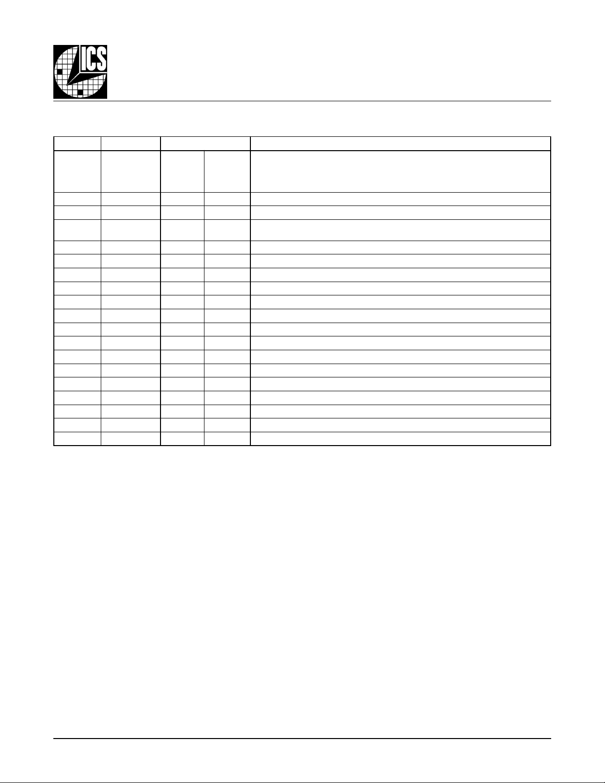
TABLE 1. PIN DESCRIPTIONS
rebmuNemaNepyTnoitpircseD
,11,1
,42,41
,53,52
84,83
3,211Qn,11QtuptuO.slevelecafretniLTSHVL.riaptuptuolaitnereffiD
5,401Qn,01QtuptuO.slevelecafretniLTSHVL.riaptuptuolaitnereffiD
,91,6
34,03
8,79Qn,9QtuptuO.slevelecafretniLTSHVL.riaptuptuolaitnereffiD
01,98Qn,8QtuptuO.slevelecafretniLTSHVL.riaptuptuolaitnereffiD
31,21CCVrewoP.V3.3ottcennoC.snipylppusevitisoP
61,517Qn,7QtuptuO.slevelecafretniLTSHVL.riaptuptuolaitnereffiD
81,716Qn,6QtuptuO.slevelecafretniLTSHVL.riaptuptuolaitnereffiD
12,025Qn,5QtuptuO.slevelecafretniLTSHVL.riaptuptuolaitnereffiD
32,224Qn,4QtuptuO.slevelecafretniLTSHVL.riaptuptuolaitnereffiD
72,623Qn,3QtuptuO.slevelecafretniLTSHVL.riaptuptuolaitnereffiD
92,822Qn,2QtuptuO.slevelecafretniLTSHVL.riaptuptuolaitnereffiD
63KLCtupnInwodlluP.tupnikcolclaitnereffidgnitrevninoN
73KLCntupnIpulluP.tupnikcolclaitnereffidgnitrevnI
04,9351Qn,51QtuptuO.slevelecafretniLTSHVL.riaptuptuolaitnereffiD
24,1441Qn,41QtuptuO.slevelecafretniLTSHVL.riaptuptuolaitnereffiD
54,4431Qn,31QtuptuO.slevelecafretniLTSHVL.riaptuptuolaitnereffiD
74,6421Qn,21QtuptuO.slevelecafretniLTSHVL.riaptuptuolaitnereffiD
:ETON
pulluP
OCCVrewoP.V8.1ottcennoC.snipylppustuptuO
EEVrewoP.dnuorgottcennoC.snipylppusevitageN
dna
nwodlluP
ICS8520
LOW SKEW, 1-TO-16
DIFFERENTIAL-TO-3.3V LVHSTL FANOUT BUFFER
.seulavlacipytrof,scitsiretcarahCniP,2elbaTeeS.srotsisertupnilanretniotsrefer
ICS8520DY www.icst.com/products/hiperclocks.html REV. B JULY 5, 2001
2
Page 3
PRELIMINARY
Integrated
Circuit
Systems, Inc.
LOW SKEW, 1-TO-16
ICS8520
DIFFERENTIAL-TO-3.3V LVHSTL FANOUT BUFFER
TABLE 2. PIN CHARACTERISTICS
lobmySretemaraPsnoitidnoCtseTmuminiMlacipyTmumixaMstinU
NICecnaticapaCtupnIKLCn,KLC4Fp
PULLUPRrotsiseRpulluPtupnI 15KΩ
NWODLLUPRrotsiseRnwodlluPtupnI 15KΩ
TABLE 3. FUNCTION TABLE
stupnIstuptuO
KLCKLCn51Qurht0Q51Qnurht0Qn
01 WOLHGIHlaitnereffiDotlaitnereffiDgnitrevnInoN
10 HGIHWOLlaitnereffiDotlaitnereffiDgnitrevnInoN
01ETON;desaiBWOLHGIHlaitnereffiDotdednEelgniSgnitrevnInoN
11ETON;desaiBHGIHWOLlaitnereffiDotdednEelgniSgnitrevnInoN
1ETON;desaiB0HGIHWOLlaitnereffiDotdednEelgniSgnitrevnI
1ETON;desaiB1WOLHGIHlaitnereffiDotdednEelgniSgnitrevnI
1.0adnadnuorgoteulavlauqeforotsisera,CCVot µ sitniophctiwsgnitluserehT.dnuorgottupniehtmorfroticapacF
.Vm003±2/CCVyletamixorppa
edoMtuptuOottupnIytiraloP
ehtstestupnidesaibehttaegatlovehT.desaibebstupnilaitnereffidehtfoenotahtseriuqeresudedneelgniS:1ETON
rotsiserasikrowtensaibtupnidednemmocerehtslevelLTTVLdnaSOMCVLroF.tupnidedneelgnisehtroftniophctiws
ICS8520DY www.icst.com/products/hiperclocks.html REV. B JULY 5, 2001
3
Page 4

PRELIMINARY
Integrated
Circuit
Systems, Inc.
LOW SKEW, 1-TO-16
ICS8520
DIFFERENTIAL-TO-3.3V LVHSTL FANOUT BUFFER
ABSOLUTE MAXIMUM RATINGS
Supply Voltage, VCCx 4.6V
Inputs, V
Outputs, V
Package Thermal Impedance, θ
Storage T emperature, T
Stresses beyond those listed under Absolute Maximum Ratings may cause permanent damage to the device. These ratings are
stress specifications only. Functional operation of product at these conditions or any conditions beyond those listed in the
Characteristics
affect product reliability .
TABLE 4A. POWER SUPPLY DC CHARACTERISTICS, VCC = 3.3V±5%, VCCO = 1.8V±0.2V, TA = 0°C TO 70°C
CCVegatloVylppuSevitisoP 531.33.3564.3V
EEItnerruCylppuSrewoP 021Am
I -0.5V to VCC+0.5 V
O -0.5V to VCC+0.5V
JA 46°C/W (no air flow)
STG -65°C to 150°C
DC
or
AC Characteristics
lobmySretemaraPsnoitidnoCtseTmuminiMlacipyTmumixaMstinU
OCCVegatloVylppuStuptuO 6.18.10.2V
is not implied. Exposure to absolute maximum rating conditions for extended periods may
TABLE 4B. DIFFERENTIAL DC CHARACTERISTICS, VCC = 3.3V±5%, VCCO = 1.8V±0.2V, TA = 0°C TO 70°C
lobmySretemaraPsnoitidnoCtseTmuminiMlacipyTmumixaMstinU
HIItnerruChgiHtupnIKLCV564.3=CCV=NIV051Aµ
KLCnV564.3=CCV=NIV1Aµ
LIItnerruCwoLtupnIKLCV564.3=CCV,V0=NIV1-Aµ
KLCnV564.3=CCV,V0=NIV051-Aµ
PPVegatloVtupnIkaeP-ot-kaeP51.03.1V
RMCV
2,1ETON
;egnaRegatloVedoMnommoC
.HIVsadenifedsiegatlovedomnommoC:1ETON
5.0+EEV58.0-CCVV
.V3.0+CCVsiKLCn,KLCrofegatlovtupnimumixameht,snoitacilppadedneelgnisroF:2ETON
TABLE 4C. LVHSTL DC CHARACTERISTICS, VCC = 3.3V±5%, VCCO = 1.8V±0.2V, TA = 0°C TO 70°C
lobmySretemaraPsnoitidnoCtseTmuminiMlacipyTmumixaMstinU
tuptuO
HOV
LOV
XOV
;egatloVhgiH
1ETON
tuptuO
;egatloVwoL
1ETON
tuptuO
egatloVrevossorC
05htiwdetanimretstuptuO:1ETON Ω .dnuorgot
0.12.1V
04.0V
LOV+)LOV-HOV(x%04LOV+)LOV-HOV(x%06V
ICS8520DY www.icst.com/products/hiperclocks.html REV. B JULY 5, 2001
4
Page 5

PRELIMINARY
Integrated
Circuit
Systems, Inc.
LOW SKEW, 1-TO-16
ICS8520
DIFFERENTIAL-TO-3.3V LVHSTL FANOUT BUFFER
TABLE 5. AC CHARACTERISTICS, VCC = 3.3V±5%, VCCO = 1.8V±0.2V, TA = 0°C TO 70°C
lobmySretemaraPsnoitidnoCtseTmuminiMlacipyTmumixaMstinU
XAMfycneuqerFtupnImumixaM 005zHM
DPt1ETON;hgiH-ot-woL,yaleDnoitagaporP 0<f≤ zHM0521 6.1sn
)o(kst4,2ETON;wekStuptuO 05sp
)pp(kst4,3ETON;wekStraP-ot-traP 052sp
RtemiTesiRtuptuOzHM05@%08ot%02003007sp
FtemiTllaFtuptuOzHM05@%08ot%02003007sp
cdoelcyCytuDtuptuO 7435%
esiwrehtodetonsselnuzHM052taderusaemsretemarapllA
.tniopgnissorctupuolaitnereffidehtottniopgnissorctupnilaitnereffidehtmorfderusaeM:1ETON
.snoitidnocdaollauqehtiwdnaegatlovylppusemasehttastuptuoneewtebwekssadenifeD:2ETON
.stniopssorclaitnereffidtuptuoehttaderusaeM
segatlovylppusemasehttagnitareposecivedtnereffidnostuptuoneewtebwekssadenifeD:3ETON
laitnereffidehttaderusaemerastuptuoeht,ecivedhcaenostupnifoepytemasehtgnisU.snoitidnocdaollauqehtiwdna
.stniopssorc
.56dradnatSCEDEJhtiwecnadroccanidenifedsiretemarapsihT:4ETON
ICS8520DY www.icst.com/products/hiperclocks.html REV. B JULY 5, 2001
5
Page 6

PRELIMINARY
Integrated
Circuit
Systems, Inc.
FIGURE 1A, 1B, 1C - INPUT CLOCK WAVEFORMS
VCC
CLK
VPP
nCLK
GND
FIGURE 1A - L VDS, HSTL, SSTL DIFFERENTIAL INPUT LEVELS
ICS8520
LOW SKEW, 1-TO-16
DIFFERENTIAL-TO-3.3V LVHSTL FANOUT BUFFER
CROSS POINTS
VCMR
VCC
CLK
nCLK
GND
VCC
GND
VPP
CROSS POINTS
FIGURE 1B - LVPECL DIFFERENTIAL INPUT LEVEL
CLK
or
nCLK
FIGURE 1C- LVCMOS AND LVTTL SINGLE ENDED INPUT LEVEL
VCMR
ICS8520DY www.icst.com/products/hiperclocks.html REV. B JULY 5, 2001
6
Page 7

PRELIMINARY
Integrated
Circuit
Systems, Inc.
PACKAGE OUTLINE - Y SUFFIX
ICS8520
LOW SKEW, 1-TO-16
DIFFERENTIAL-TO-3.3V LVHSTL FANOUT BUFFER
TABLE 6. PACKAGE DIMENSIONS
LOBMYS
N
A
1A
2A
b
c
D
1D
2D
E
1E
2E
e
L
q
ccc
MUMINIMLANIMONMUMIXAM
----06.1
50.0--51.0
53.104.154.1
71.022.072.0
90.0--02.0
54.006.057.0
0
°
----80.0
NOITAIRAVCEDEJ
SRETEMILLIMNISNOISNEMIDLLA
CBB
84
CISAB00.9
CISAB00.7
.feR05.5
CISAB00.9
CISAB00.7
.feR05.5
CISAB05.0
--
7
°
Reference Document: JEDEC Publication 95, MS-026
ICS8520DY www.icst.com/products/hiperclocks.html REV. B JULY 5, 2001
7
Page 8

PRELIMINARY
Integrated
Circuit
Systems, Inc.
ORDERING INFORMATION
YD0258SCIYD0258SCIPFQLdaeL84yartrep052C°07otC°0
TYD0258SCIYD0258SCIleeRdnaepaTnoPFQLdaeL840001C°07otC°0
ICS8520
LOW SKEW, 1-TO-16
DIFFERENTIAL-TO-3.3V LVHSTL FANOUT BUFFER
rebmuNredrO/traPgnikraMegakcaPtnuoCerutarepmeT
While the information presented herein has been checked for both accuracy and reliability, Integrated Circuit Systems, Incorporated (ICS) assumes no responsibility for either its use
or for infringement of any patents or other rights of third parties, which would result from its use. No other circuits, patents, or licenses are implied. This product is intended for use
in normal commercial applications. Any other applications such as those requiring extended temperature range, high reliability, or other extraordinary environmental requirements are
not recommended without additional processing by ICS. ICS reserves the right to change any circuitry or specifications without notice. ICS does not authorize or warrant any ICS
product for use in life support devices or critical medical instruments.
ICS8520DY www.icst.com/products/hiperclocks.html REV. B JULY 5, 2001
8
 Loading...