

Page 1
Integrated
Circuit
Systems, Inc.
ICS8501
LOW SKEW 1-TO-16 DIFFERENTIAL
CURRENT MODE FANOUT B UFFER
GENERAL DESCRIPTION
The ICS8501 is a low skew, 1-to-16 Differential
,&6
HiPerClockS™
to small swing differential current mode(DCM) output levels.
An external reference resistor is used to set the value of the
current supplied to an external load load/termination resistor. The load resistor value is chosen to equal the value of
the characteristic line impedance of 50Ω. The ICS8501 is char-
acterized at an operating supply voltage of 3.3V.
The small swing outputs, accurate crossover voltage and duty
cycle makes the ICS8501 ideal for interfacing to todays most
advanced microprocessors.
Current Mode Fanout Buffer and a member of
the HiPerClockS family of High Performance
Clock Solutions from ICS. The ICS8501 is designed to translate any differential signal levels
FE ATURES
• 16 small swing DCM outputs
• Translates any differential input signal(PECL, HSTL, LVDS,
DCM) to DCM levels without external bias networks
• Translates single ended input levels to DCM levels with a
resistor bias network on the nCLK input
• Translates single ended input levels to inverted DCM levels
with a resistor bias network on the CLK input
• Voh(max) = 1.2V
• 40% of Voh ≤ Vcrossover ≤ 60% of Voh
• 45% ≤ Duty Cycle ≤ 55%
• Output frequency up to 500MHz
• 100ps output skew
• 3.3V operating supply
• 48 lead low-profile QFP(LQFP), 7mm x 7mm x 1.4mm
package body, 0.5mm package lead pitch
• 0°C to 70°C ambient operating temperature
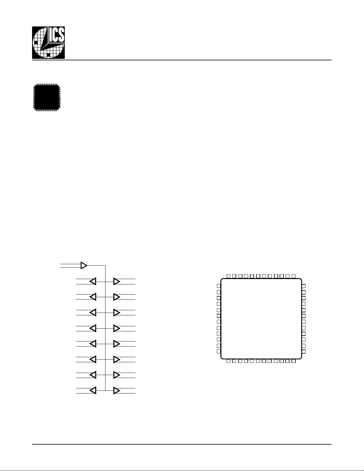
BLOCK DIAGRAM PIN ASSIGNMENT
CLK
nCLK
Q0
nQ0
Q1
nQ1
Q2
nQ2
Q3
nQ3
Q4
nQ4
Q5
nQ5
Q6
nQ6
Q7
nQ7
Q15
nQ15
Q14
nQ14
Q13
nQ13
Q12
nQ12
Q11
nQ11
Q10
nQ10
Q9
nQ9
Q8
nQ8
VCC
Q11
nQ11
Q10
nQ10
GND
Q9
nQ9
Q8
nQ8
VCC
nc
nQ12
nQ13
VCC
Q12
48 47 46 45 44 43 42 41 40 39 38 37
1
2
3
4
5
6
7
8
9
10
11
12
13 14 15 16 17 18 19 20 21 22 23 24
Q7
VCC
RREF
GND
Q13
ICS8501
nQ6
Q6
nQ7
nQ14
GND
Q14
Q5
nQ15
nQ5
Q15
Q4
nQ4
48-Lead LQFP
Y Package
Top View
VCC
nCLK
36
35
34
33
32
31
30
29
28
27
26
25
VCC
CLK
VCC
nQ0
Q0
nQ1
Q1
GND
nQ2
Q2
nQ3
Q3
VCC
8501 www.icst.com REV. A - AUGUST 23, 2000
1
Page 2
Integrated
Circuit
Systems, Inc.
TABLE 1. PIN DESCRIPTIONS
rebmuNemaNepyTnoitpircseD
,11,1
,42,41
,53,52
84,83
3,211Qn,11QtuptuO .slevelecafretniedomtnerruclaitnereffiD.tuptuolaitnereffiD
5,401Qn,01QtuptuO .slevelecafretniedomtnerruclaitnereffiD.tuptuolaitnereffiD
,91,6
34,03
8,79Qn,9QtuptuO .slevelecafretniedomtnerruclaitnereffiD.tuptuolaitnereffiD
01,98Qn,8QtuptuO .slevelecafretniedomtnerruclaitnereffiD.tuptuolaitnereffiD
21cndesunU.noitcennocoN
31FERRtupnI
61,517Qn,7QtuptuO .slevelecafretniedomtnerruclaitnereffiD.tuptuolaitnereffiD
81,716Qn,6QtuptuO .slevelecafretniedomtnerruclaitnereffiD.tuptuolaitnereffiD
12,025Qn,5QtuptuO .slevelecafretniedomtnerruclaitnereffiD.tuptuolaitnereffiD
32,224Qn,4QtuptuO .slevelecafretniedomtnerruclaitnereffiD.tuptuolaitnereffiD
72,623Qn,3QtuptuO .slevelecafretniedomtnerruclaitnereffiD.tuptuolaitnereffiD
92,822Qn,2QtuptuO .slevelecafretniedomtnerruclaitnereffiD.tuptuolaitnereffiD
63KLCtupnI .slevelecafretnitupnilaitnereffidynA.tupnikcolclaitnereffidgnitrevninoN
73KLCntupnI .slevelecafretnitupnilaitnereffidynA.tupnikcolclaitnereffidgnitrevnI
04,9351Qn,51QtuptuO .slevelecafretniedomtnerruclaitnereffiD.tuptuolaitnereffiD
24,1441Qn,41QtuptuO .slevelecafretniedomtnerruclaitnereffiD.tuptuolaitnereffiD
54,4431Qn,31QtuptuO .slevelecafretniedomtnerruclaitnereffiD.tuptuolaitnereffiD
74,6421Qn,21QtuptuO .slevelecafretniedomtnerruclaitnereffiD.tuptuolaitnereffiD
CCVrewoP.V3.3ottcennoC.nipylppusrewoP
DNGrewoP.dnuorgottcennoC.nipylppusrewoP
ICS8501
LOW SKEW 1-TO-16 DIFFERENTIAL
CURRENT MODE FANOUT B UFFER
574ottcennoC.tnerructuptuoehttesotdesU.tupnitnerrucecnerefeR Ω
.dnuorgotrotsiser
TABLE 2. PIN CHARACTERISTICS
lobmySretemaraPsnoitidnoCtseTmuminiMlacipyTmumixaMstinU
NICecnaticapaCtupnI 2Fp
DPC
TUORecnadepmItuptuO 41KΩ
)tuptuorep(
ecnaticapaCnoitapissiDrewoP
zHM052=f,V564.3=CCV6.4Fp
TABLE 3. FUNCTION T ABLE
stupnIstuptuO
KLCKLCn51Qurht0Q51Qnurht0Qn
01 0 1 laitnereffiDotlaitnereffiDgnitrevnInoN
10 1 0 laitnereffiDotlaitnereffiDgnitrevnInoN
01ETON;desaiB01 laitnereffiDotdednEelgniSgnitrevnInoN
11ETON;desaiB10 laitnereffiDotdednEelgniSgnitrevnInoN
1ETON;desaiB010 laitnereffiDotdednEelgniSgnitrevnI
1ETON;desaiB101 laitnereffiDotdednEelgniSgnitrevnI
1.0adnadnuorg µ .Vm003±2/CCVyletamixorppasitniophctiwsgnitluserehT.dnuorgottupniehtmorfroticapacF
8501 www.icst.com REV. A - AUGUST 23, 2000
2
edoMtuptuOottupnIytiraloP
ehtroftniophctiwsehtstestupnidesaibehttaegatlovehT.desaibebstupnilaitnereffidehtfoenotahtseriuqeresudedneelgniS:1ETON
oteulavlauqeforotsisera,CCVotrotsiserasikrowtensaibtupnidednemmocerehtslevelLTTVLdnaSOMCVLroF.tupnidedneelgnis
Page 3
Integrated
Circuit
Systems, Inc.
LOW SKEW 1-TO-16 DIFFERENTIAL
CURRENT MODE FANOUT B UFFER
ICS8501
ABSOLUTE MAXIMUM RATINGS
Supply Voltage 4.6V
Inputs -0.5V to VCC+0.5 V
Outputs -0.5V to VCC+0.5V
Ambient Operating Temperature 0°C to 70°C
Storage Temperature -65°C to 150°C
Stresses beyond those listed under Absolute Maximum Ratings may cause permanent damage to the device. These ratings are stress specifications
only and functional operation of the device at these or any conditions beyond those listed in the DC Electrical Characteristics or AC Electrical
Characteristics is not implied. Exposure to absolute maximum rating conditions for extended periods may affect product reliability.
TABLE 4. DC ELECTRICAL CHARACTERISTICS, VCC = 3.3V±5%, TA = 0°C TO 70°C
lobmySretemaraPsnoitidnoCtseTmuminiMlacipyTmumixaMstinU
CCVegatloVylppuSgnitarepO 531.33.3564.3V
PPVegatloVtupnIkaeP-ot-kaeP 13.03.1V
RMCV
HIItnerruChgiHtupnIKLCn,KLCCCV=NIV5Aµ
LIItnerruCwoLtupnIKLCn,KLCV0=NIV5-Aµ
CCItnerruCylppuSgnitarepO 07Am
HOI2ETON;tnerruCtuptuOV531.3 ≤ CCV ≤ V564.3114171Am
HOVegatloVhgiHtuptuO574=FERR Ω 05=DAOLR, Ω 6.017.02.1V
LOVegatloVwoLtuptuO574=FERR Ω 05=DAOLR, Ω 050.0V
1ETON
.B1dnaA1erugiFeeS.egatlov
;egatloVtupnIedoMnommoC
.CCIsulp61semitHOIotlauqesi)latot(CCI
sleveLLCEPVL8.14.2V
sleveLLTSS,SDVL,LTSH,MCD13.03.1V
revossorcehtsadenifedsiLTSSdnaSDVL,LTSH,MCDrofegatlovtupniedomnommoC.CCVhtiw1:1yravlliwLCEPVLrofRMCV
eroferehT.noitaluclactnerrucylppuslatotehtnidedulcniebdluohsdnadaolehtotdeilppusgniebtuptuoreptnerrucehtsiHOI:2ETON
.V3.3=CCVroferaA4elbaTnidetonseulavLCEPVLehT.HIVmuminimehtsadenifedsiLCEPVLrofegatlovtupniedomnommoC:1ETON
TABLE 5. AC ELECTRICAL CHARACTERISTICS, VCC = 3.3V±5%, TA = 0°C TO 70°C
lobmySretemaraPsnoitidnoCtseTmuminiMlacipyTmumixaMstinU
XAMfycneuqerFtupnImumixaM
HLpthgiH-ot-woL,yaleDnoitagaporP0< f ≤ zHM0522 3sn
LHptwoL-ot-hgiH,yaleDnoitagaporP0< f ≤ zHM0522 3sn
)o(kst3ETON;wekStuptuOXOVtanoderusaeM001sp
)pp(kst
RtemiTesiRtuptuO%08ot%02571007sp
FtemiTllaFtuptuO%08ot%02571007sp
WPthtdiWesluPtuptuO
XOVegatloVrevossorCtuptuO HOV%04HOV%06V
574slauqeFERR:2ETON .Ω 05htiwdetanimretstuptuO Ω dnuorgotdetcennocrotsiser .
8501 www.icst.com REV. A - AUGUST 23, 2000
4ETON;wekStraP-ot-traPXOVtanoderusaeM056sp
.esiwrehtodetonsselnuzHM052taderusaemsretemarapllA:1ETON
3
ehtfoffollorBd3-ehttaderusaeM
egatlovtuptuokaep-ot-kaep
2/ELCYCt
3.0-
.snoitidnocdaollauqehtiwdnasegatlovylppusemasehttastuptuossorcawekssadenifeD:3ETON
2/ELCYCt
005zHM
2/ELCYCt
3.0+
.snoitidnocdaollauqehtiwdnasegatlovylppusemasehttagnitareposecivedtnereffidnostuptuotnereffidtawekssadenifeD:4ETON
sn
Page 4

Integrated
Circuit
Systems, Inc.
FIGURE 1A, 1B, 1C - INPUT CLOCK WAVEFORMS
VCC
CLK
ICS8501
LOW SKEW 1-TO-16 DIFFERENTIAL
CURRENT MODE FANOUT B UFFER
nCLK
GND
VCC
CLK
nCLK
GND
VPP
CROSS POINTS
VCMR
FIGURE 1A - DCM, LVDS, HSTL, SSTL DIFFERENTIAL INPUT LEVELS
VPP
CROSS POINTS
VCMR
FIGURE 1B - LVPECL DIFFERENTIAL INPUT LEVEL
VCC
CLK
or
nCLK
GND
FIGURE 1C- LVCMOS AND LVTTL SINGLE ENDED I NPUT LEVEL
8501 www.icst.com REV. A - AUGUST 23, 2000
4
Page 5

Integrated
Circuit
Systems, Inc.
FIGURE 2A - TIMING WAVEFORMS
CLK
nCLK
ICS8501
LOW SKEW 1-TO-16 DIFFERENTIAL
CURRENT MODE FANOUT B UFFER
Vpp
tPHL
Q0 thru Q15
nQ0 thru nQ15
tPLH
FIGURE 3A - PROPAGATION DELAYS
fin = 250MHz, Vpp = 300mV, tr = tf = 200ps
FIGURE 3A - OUTPUT SKEW D EFINITION & WAVEFORMS
Output Skew - Skew between any outputs. Outputs operating at the same temperature, supply voltages and with equal load
conditions.
CLK
Vpp
nCLK
Q0
CROSS POINTS
nQ0
Q1 thru Q15
nQ1 thru nQ15
tsk(o) tsk(o)
CROSS POINTS
FIGURE 3A - OUTPUT SKEW
fin = 250MHz, Vpp = 300mV, tr = tf = 200ps
8501 www.icst.com REV. A - AUGUST 23, 2000
5
Page 6

Integrated
Circuit
Systems, Inc.
LOW SKEW 1-TO-16 DIFFERENTIAL
CURRENT MODE FANOUT B UFFER
ICS8501
FIGURE 3B - PART-TO-PART SKEW DEFINITION & WAVEFORMS
Part-to-Part Skew - Skew between any outputs on different parts. Outputs operating at the same temperature, supply voltages
and with equal load conditions.
CLK
Vpp
nCLK
PART 1 Q0
CROSS POINTS
nQ0
PART 2 Q1 thru Q15
nQ1 thru nQ15
tsk(o)
CROSS POINTS
FIGURE 3B - PART-TO-PART SKEW
fin = 250MHz, Vpp = 300mV, tr = tf = 200ps
tsk(o)
8501 www.icst.com REV. A - AUGUST 23, 2000
6
Page 7

Integrated
Circuit
Systems, Inc.
PACKAGE OUTLINE AND DIMENSIONS - Y SUFFIX
NOTE 4
NOTE 4
D
D
NOTE 5, 7
NOTE 5, 7
D1
D1
NOTE 3
NOTE 3
-D-
-D-
NOTE 3
NOTE 3
-A-
-A-
e
e
N/4 TIPS
N/4 TIPS
0.20 C A-B D4X
0.20 C A-B D4X 0.20 C A-B D0.20 C A-B D4X
SEE DETAIL “A”
SEE DETAIL “A”
8 PLACES
8 PLACES
11 / 13°
11 / 13°
D/2
D/2
D1/2
D1/2
NOTE 3
NOTE 3
-B-
-B-
E/2
E/2
E1/2
E1/2
A
A
-H-
-H-
NOTE 2 / / 0.10 C
NOTE 2 / / 0.10 C
-C-
-C-
SEE DETAIL “B”
SEE DETAIL “B”
ccc
ccc
ICS8501
LOW SKEW 1-TO-16 DIFFERENTIAL
CURRENT MODE FANOUT B UFFER
e / 2
e / 2
-A, B, OR -D-
-A, B, OR -D-
b
b
E
E1
E
E1
N
N
N
N
O
O
O
O
T
T
T
T
E
E
E
E
5,
5,
4
4
7
7
NOTES:
1. ALL DIMENSIONS AND TOLE RANCING CONFORM T O ANSI
Y14.5-1982
2. DATUM PLANE -H-LOCATED AT MOLD PARTING LINE AND
COINCIDENT WITH LEAD, WHERE LEAD EXITS PLASTIC BODY
AT BOTTOM OF PARTING LINE.
3. DATUMS A-B AND -D- TO BE DETERMINED AT CENT ERLINE
BETWEEN LEADS WHERE LEADS EXIT PLASTIC AT DAT UM
PLANE -H- .
4. TO BE DETERM INED AT SEATING PLACE -C- .
5. DIM ENSIONS D1 AND E1 DO NOT INCLUDE MOLD
PROT RUSION.
6. “N” IS THE TOTAL NUMBER OF TERMINALS.
7. THESE DIMENS IONS TO BE DETEREMINED AT DATUM PLANE
-H-.
8. PACKAGE TOP DIMENSIONS ARE SMALLER THAN BOTTOM
DIM ENSIONS AND T OP OF PACKAGE WILL NOT OVERHANG
BOTTOM OF PACKAGE.
9. DIM ENSION b DOES NOT INCLUDE DA MBAR PROT RUSION.
ALLOWABLE DAMBAR PROTRUSION SHALL BE 0.08mm T OTAL
IN EXCESS OF THE b DIMENSION AT MAXIMUM MATERIAL
CONDITION.
10. CO NT ROLLI NG DIMENSION: MILLIMETER.
11. THIS OUTLI NE CO NF ORMS TO JE DEC PUBLIBCAT ION 95
REGISTRATION M S- 026, VARIATION BB C.
12. A1 IS DEFINED AS THE DISTANCE FROM T HE SEATING PLANE
TO THE LOWEST POINT OF THE PACKAGE.
-A, B, OR -D-
-A, B, OR -D-
b
b
b
b
1
1
0.08
0.08
R. MIN.
R. MIN.
0.20 MIN.
0.20 MIN.
1.00 REF.
1.00 REF.
ddd M C A-B S D S
WITH LEAD FINISH
WITH LEAD FINISH
BASE METAL
BASE METAL
0° MIN.
0° MIN.
0° -7 °
0° -7 °
L
L
0.08/0.20 R.
0.08/0.20 R.
0.25
0.25
GAUGE PLANE
GAUGE PLANE
S
A
A
D
E
b1
b1
ccc
ccc
ddd
ddd
S
Y
Y
M
M
B
B
O
O
L
L
A
A
A
1
1
A
2
2
D
D
D
1
1
E
E
E
1
1
L
L
N
N
e
e
b
b
JEDEC VARIATION
JEDEC VARIATION
ALL DIM E NSIONS IN MILLIMETERS
ALL DIM E NSIONS IN MILLIMETERS
MIN. NOM. MAX.
MIN. NOM. MAX.
0.05 0.15
0.05 0.15
1.35 1.40 1.45
1.35 1.40 1.45
9.00 BSC.
9.00 BSC.
7.00 BSC.
7.00 BSC.
9.00 BSC.
9.00 BSC.
7.00 BSC.
7.00 BSC.
0.45 0.60 0.75
0.45 0.60 0.75
0.5 BSC.
0.5 BSC.
0.17 0.22 0.27
0.17 0.22 0.27
0.17 0.20 0.23
0.17 0.20 0.23
BBC
BBC
48
48
1.60
1.60
0.08
0.08
0.08
0.08
12
12
7, 8
7, 8
7, 8
7, 8
N
N
O
O
T
T
E
E
4
4
4
4
9
9
NOTE 9 ddd M C A-B S D S
NOTE 9
0.09 / 0.20 0.09 / 0.16
0.09 / 0.20 0.09 / 0.16
-0.05 S
-0.05 S
-0.05 S
DATUM
DATUM
A2
A2
PLANE
PLANE
-H-
-H-
A1
A1
8501 www.icst.com REV. A - AUGUST 23, 2000
7
Page 8

Integrated
Circuit
Systems, Inc.
ORDERING INFORMATION
YB1058SCIYB1058SCIPFQLdaeL84yartrep052C°07otC°0
TYB1058SCIYB1058SCIleeRdnaepaTnoPFQLdaeL840002C°07otC°0
ICS8501
LOW SKEW 1-TO-16 DIFFERENTIAL
CURRENT MODE FANOUT B UFFER
rebmuNredrO/traPgnikraMegakcaPtnuoCerutarepmeT
While the information presented herein has been checked for both accuracy and reliability, Integrated Circuit Systems, Incorporated (ICS) assumes no responsibility for either its
use or for infringement of any patents or other rights of third parties, which would result from its use. No other circuits, patents, or licenses are implied. This product is intended for
use in normal commercial applications. Any other applications such as those requiring extended temperature range, high reliability, or other extraordinary environmental
requirements are not recommended without additional processing by ICS. ICS reserves the right to change any circuitry or specifications without notice. ICS does not authorize
or warrant any ICS product for use in life support devices or critical medical instruments.
8501 www.icst.com REV. A - AUGUST 23, 2000
8
 Loading...