

Page 1
HV9906 FlexSwitch
(Simple Off-Line/PFC & >9V DC/DC Switcher)
Features
Drive one or hundreds of LEDs including White LEDs
Programmable Current Source (mA to A)
Programmable Voltage Source (Steps Up or Down)
Integrator Lock Loop Technology (IL
o Built in Soft Start
o Allows Discontinuous Feedback
o Eliminates Compensation Components
o Eliminates Output Averaging Filters
o Inherent Dither to Reduce EMI
Eliminates High Voltage Input Electrolytic Capacitor
Smallest and Most Reliable Off-Line Solution
Isolated or Non-Isolated Applications
Can be Operated Directly from Rectified AC Mains
10V to 400V Input Range Internal Regulator
<1.5mA Operating Supply Current
Programmable Feed Forward Regulation
Programmable Feedback Sense Threshold (mV to V)
Integrating Differential Sense Feedback
Seamlessly Change from AC to Battery Operation
Applications
LED driver
Power Factor Correction
Constant Current or Voltage Source
Battery Charger / PWM Housekeeping Supplies
Traffic Lights / Street Lights
Back Lighting of Flat Panel Displays
Advertising Signs
Automotive
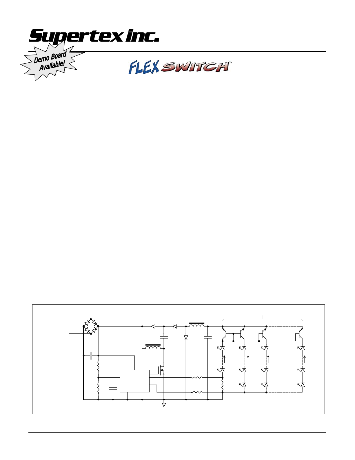
Typical Application Circuit
2
)
HV9906
TM
Initial Release
General Description
The Supertex HV9906 allows the development of the smallest
possible, most reliable, offline and wide DC/DC conversion range
converters for driving LEDs and other applications. The HV9906
combines internally all the components required to operate directly
from the rectified AC line with a feedback mechanism that
eliminates filters & compensation components, and which can
close the loop with feedback from a discontinuous waveform (eg.
LED current).
The HV9906 is capable of driving multiconverters, which have
been shown to provide the best performance to component count
trade off for wide conversion range applications like offline
converters. Applicable multiconverters include bucking & boosting
topologies, in isolated & non-isolated configurations, as well as
power factor correcting topologies from <1W up to 150W.
Proper choice of external components will allow the programming
of currents from <1mA to several amps and will allow stepping up
or stepping down from the input without the need to change
components. For example, the same HV9906 converter nominally
regulating to 60VDC output may operate from 12VDC, or from
rectified AC input to 265V
The HV9906 utilizes a programmable inversely proportional fast
feed forward algorithm to calculate output on time and a novel
Integrating Lock Loop (IL
differential sensing. The sensed feedback may be positive or
negative with respect to ground and the signal may be
discontinuous. In some topologies this control method permits the
elimination of the bulky input filter capacitor (a small high voltage
ceramic or film capacitor is required to maintain a high frequency
path). This algorithm when used with certain multiconverters such
as the flyback-buck, with a fixed load, results in near constant
frequency with only a small dither which helps meet FCC
requirements.
.
RMS
2
) feedback with programmable threshold
NPN Bipolar Transistor Array or Matched 2N2222
Q1 Q2 Q3 Q25
Negative Voltage
-
+
100
LED-1
Row 1
20mA
LED-9
Row 1
R5
LED-1
Row 2
20mA
LED-9
Row 2
LED-10
Row 2
LED-1
Row 3
20mA
LED-9
Row 3
LED-10
Row 3
LED-1
Row 25
20mA
LED-9
Row 25
LED-10
Row 25
12VDC to 400VDC
or
65VAC to 280VAC
1N4007
D1 D2
D4 D3
C1
0.047uF
400V
R1
8M
R2
100k
1uF
to
6.8uF
D5
MURS160
C3 C4
0.033uF
L1
56uH
U1
+Vin
GATE
HV9906
NS
PS
PGND
Von
Vdd
C2
AGND
D6
MURS160
MURS160
M1
IRFBC30AF
L2
15uH
D7
Optional
R3
900k
R4
300k
1 07/23/02
Supertex, Inc. 1235 Bordeaux Drive, Sunnyvale, CA 94089 TEL: (408) 744-0100 FAX: (408) 222-4895 www.supertex.com
Page 2
HV9906
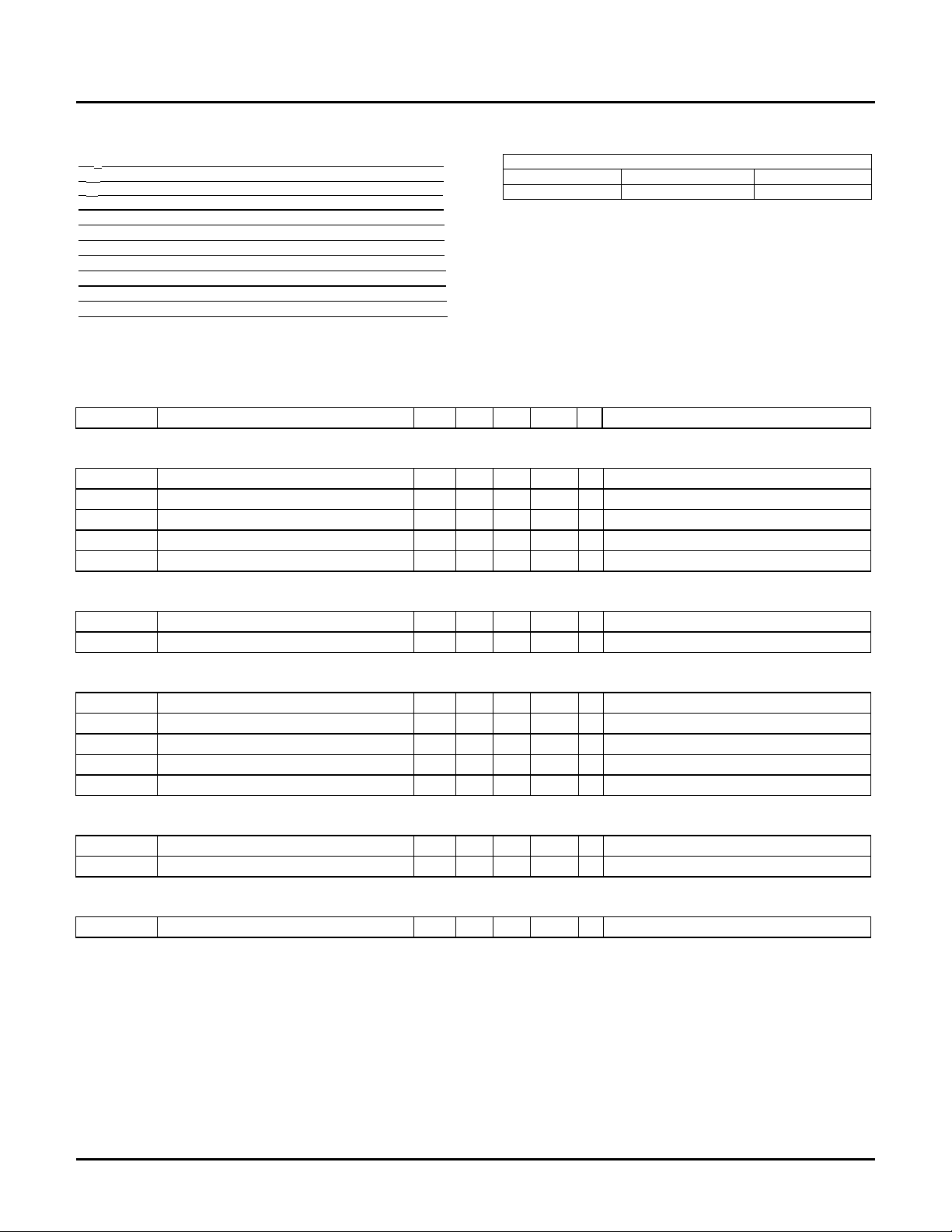
Absolute Maximum Ratings*
Input Voltage -0.3V to +450V
+V
IN
-0.3V to +15V
V
DD
Pulse Width Control Voltage -0.3 to +10V
V
ON
PS & NS Pin Feedback Voltage -0.3V to +10V
Operating Ambient Temperature Range -40°C to +85°C
Operating Junction Temperature Range -40°C to +150°C
Storage Temperature Range -65°C to +150°C
Thermal Resistance Junction to Ambient, SOIC 159°C/W
Thermal Resistance Junction to Case, SOIC 45°C/W
Thermal Resistance Junction to Ambient, Plastic DIP 110°C/W
Thermal Resistance Junction to Case, Plastic DIP 35°C/W
*All voltages referenced to AGND and PGND connected together.
Electrical Characteristics (Unless otherwise noted T
Symbol Parameter Min Typ Max Units T
Input Regulator/Vdd Supply
+V
IN
+I
IN
V
DD(REG)
V
Under Voltage Lockout Threshold 8.0 V Decaying VDD
UVLO
V
Under Voltage Lockout Hysteresis 0.50 V
HYST
MOSFET Gate Drive Output
t
R
t
F
PWM
P(VON)
P(VON) Output Pulse Width at VON 2 3.35 uSec VON = 0.2V
P
Maximum Output Pulse Width 17.8 uSec VON = 0V
MAX
f
Minimum Output Frequency 10 13.5 17 KHz
MIN
f
Maximum Output Frequency 250 450 KHz
MAX
Current Sense
V
PS
V
NS
Pulse Width Control Feed Forward Voltage
V
ON
The “*” denotes specifications that apply over the full temperature range (-40°C to +85°C)
Input Voltage 8.5 400 V * Typical under UVLO
Input Current 1.5 mA * Gate pin open and operating at F
Internal Regulator Output Voltage 10 11 V *
Rise Time 75 nSec C
Fall Time 75 nSec C
Output Pulse Width at VON 215 300 nSec VON = 5.0V
Positive Sense Pin Voltage 0.9 1 1.1 V * Note: VPS and VNS are matched
Negative Sense Pin Voltage 0.9 1 1.1 V * Note: VPS and VNS are matched
Effective Pulse Width Control Voltage Range 0.2 6.0 V *
= 25°C)
A
Ordering Information
8 Pin Plastic DIP 8 Pin SOIC Dice
HV9906P HV9906LG HV9906X
A
GATE
GATE
Package Options
Conditions
= 750pF
= 750pF
MAX
2 07/23/02
Supertex, Inc. 1235 Bordeaux Drive, Sunnyvale, CA 94089 TEL: (408) 744-0100 FAX: (408) 222-4895 www.supertex.com
Page 3
HV9906
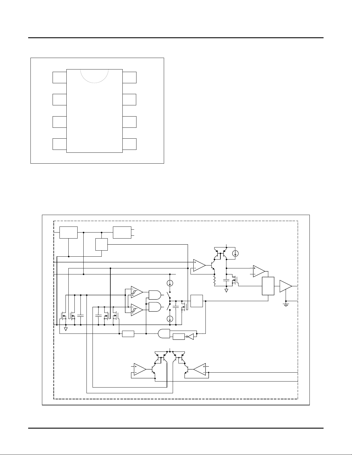
Pinout
Pin Description
– This pin is the input to the internal linear regulator.
+V
IN
–The voltage applied to this pin by a resistor voltage divider
V
ON
+Vin
GATE
1
8
from +V
V
controls the on time (pulse width) of the gate output.
IN
– This pin is the output of the internal linear regulator and the
DD
supply pin for the internal circuits. It must be bypassed with a low
Von PGND
2
7
HV9906
Vdd
3
NS
6
ESR capacitor to provide a low impedance path for the gate drive
and be capable of storing sufficient energy so that the voltage does
not decay below the UVLO threshold during the time when the
input voltage is below the minimum required by the regulator.
AGND – This pin is the common connection for analog circuits.
GATE – This pin is the output for driving the gate of an external N-
channel MOSFET.
AGND PS
45
PGND – This is the common connection for the GATE drive circuit.
NS – This pin is the negative terminal of the differential sense
feedback circuit.
PS – This pin is the positive terminal of the differential sense
feedback circuit.
__________________________________________________________________________________________________________________
Functional Block Diagram
+Vin
Von
Vdd
AGND
High Voltage
Regulator
UVLO
and
POR
Reset Pulse
Bandgap
Reference
Delay
1V
Vref
C
C
Sample Pulse
Vdd
Vdd
Delay
VCO
Vdd
Vref
1V1V
R
_
Q
Q
Driver
S
GATE
PGND
NS
PS
3 07/23/02
Supertex, Inc. 1235 Bordeaux Drive, Sunnyvale, CA 94089 TEL: (408) 744-0100 FAX: (408) 222-4895 www.supertex.com
Page 4
Functional Description
The HV9906 consists of the following functional blocks:
High Voltage Regulator
Bandgap Reference
Under Voltage Lockout and Power On Reset
Voltage Controlled Oscillator
Feed Forward On Time Control
Differential Sense Circuit and Programmable Reference
Integrator
Sample and Hold VCO Control
Gate Driver
Soft Start
The following sections provide a detailed explanation of each of
these blocks.
High Voltage Regulator
All internal circuits operate from a nominal 10V V
provided by an onboard linear regulator capable of accepting input
voltages up to 400V. This regulator blocks reverse current flow
from V
to +VIN, such as in the case when the input voltage is a
DD
full wave rectified sine wave. Therefore, if a sufficiently large
bypass capacitor (>1µF) is connected to V
, the operation of the
DD
circuit can be maintained during the times when the full wave
rectified input voltage is less than the regulated output voltage.
High operating frequency and high input voltage applications will
result in increased power dissipation in the regulator. For these
applications efficiency may be improved by bootstrapping the V
pin if a non-isolated +10V output is available. Supertex’s high
voltage technology allows a very low current regulator, rather than
a shunt, to power the IC. This makes it possible to continuously
operate the IC from the AC line, within thermal limits & without
bootstrapping, in certain applications.
Bandgap Reference
As the regulator turns on and the V
voltage rises, a bandgap
DD
reference is activated to establish the regulation point of the
regulator and provide the required references for the internal
circuits. The references are strictly internal and not available at
any pin of the device.
Under Voltage Lockout and Power On Reset
On initial power application the high input voltage (up to 400V)
linear regulator charges the capacitor connected to V
to provide a stable supply for the internal circuitry. Under voltage
lockout (UVLO) holds the voltage controlled oscillator (VCO)
disabled until the V
supply rises above a nominal 8.5V and
DD
power on reset (POR) clamps the capacitors in the sample and
hold and integrator circuits low for a short time thereafter, thus
setting the VCO to its lowest frequency state. The UVLO has a
0.5V hysteresis to prevent false triggering due to ripple on V
Voltage Controlled Oscillator
The period of the voltage controlled oscillator (VCO) is determined
by the output of the sample and hold circuit while the feed forward
control from the V
pin provides fast direct control of the oscillator
ON
output on time. For unusual operating circumstance the VCO may
be driven to its maximum frequency and the on time may exceed
the period of the oscillator. This will cause cycle skipping or an
effective reduction in output frequency by an integer factor.
supply
DD
and seeks
DD
DD
DD
.
HV9906
Feed Forward On Time Control
The output signal to the gate driver is controlled by a latch that is
set by the output of the VCO and reset by the feed forward on time
control, thus the voltage applied to the V
continuous control of the gate drive on time. The on time is
inversely proportional to the applied voltage and there is an
internally set limit to the maximum on time (17.8µS) so that 0V will
not result in an infinite on time. Refer to “Programming On Time”
in the Design Information section.
To operate in discontinuous conduction mode with constant energy
transfer per cycle a resistor divider from the input voltage is
connected to the V
pin, thereby providing fast feed forward input
ON
regulation control. This control loop can easily track a rectified
sine wave of input voltage at 50Hz, 60Hz or 400Hz provided that
the capacitor connected at V
can store sufficient energy to
DD
prevent decay below the UVLO threshold during the time when the
rectified sine wave input voltage at +V
50Hz rectified sine wave a 3.3µF capacitor connected to V
sufficient to guarantee stable operation.
For power factor correction applications an input voltage peak
detector or a low pass filter can be used to drive the V
will provide an essentially constant on time control voltage
resulting in an energy transfer per oscillator cycle directly
proportional to the input voltage.
Differential Sense Circuit and Programmable Reference
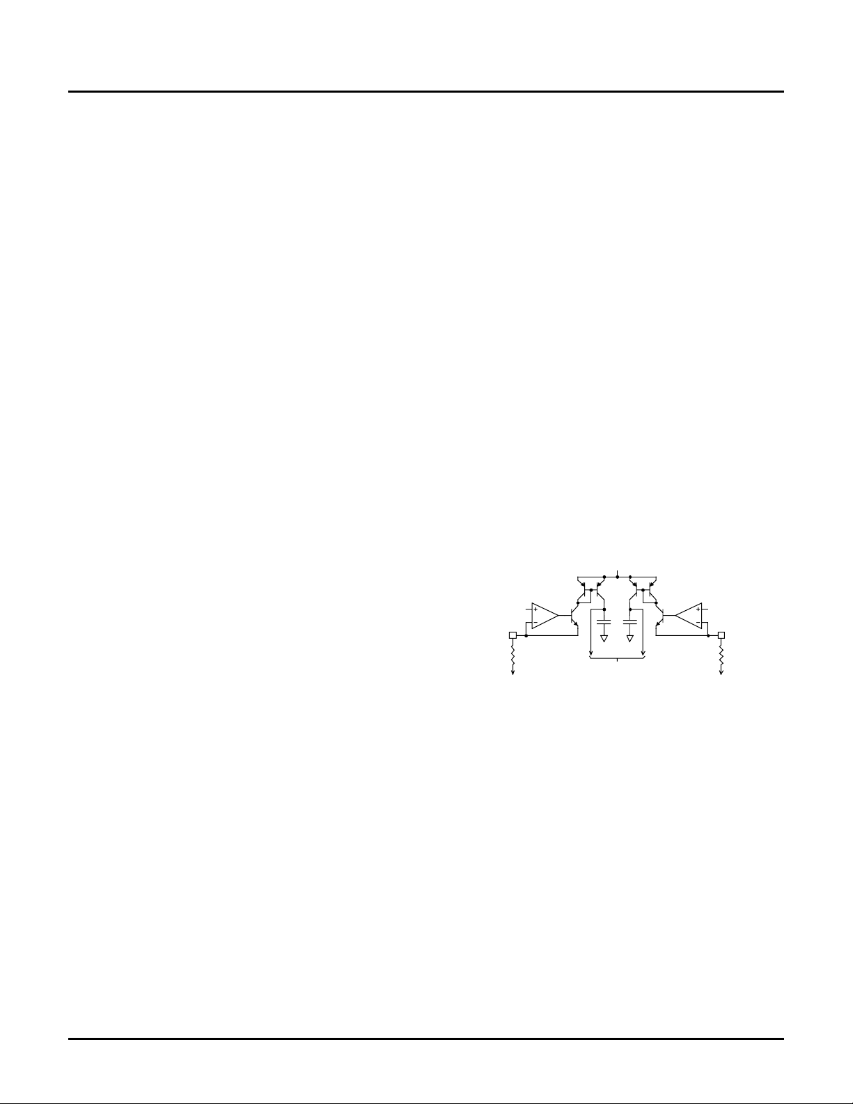
The following simplified equivalent circuit is provided to clarify the
operation and programming of this circuit.
+1V +1V
PS NS
R
To Least Negative
Sense Node
Relative to +1 Volt
Vdd
20pF
To Sample and Hold
Comparators
This differential sense circuit is typically used to monitor the output
voltage or current of a power converter. The circuit operates by
sourcing current (typically 5µA) from both the PS and NS pins
which are regulated at a nominal +1V and the control loop seeks to
maintain a sense node voltage (voltage across a current sense
resistor or the voltage across a resistor divider) that will make the
NS and PS currents equal. Regulation is established when there
is zero current difference in the PS and NS pins. This differential
common mode sense method reduces noise sensitivity and
enables the user to define the magnitude of the sensed voltage
(i.e. +100mV for high efficiency or –2.5V to escape the noise floor)
and thus the effective reference, provided the sensed nodes are at
less than +1V with respect to ground.
pin provides direct and
ON
is below 10V. For a 100V
IN
NSR PS
To Most Negative
Sense Node
Relative to +1Volt
pin. This
ON
DD
is
4 07/23/02
Supertex, Inc. 1235 Bordeaux Drive, Sunnyvale, CA 94089 TEL: (408) 744-0100 FAX: (408) 222-4895 www.supertex.com
Page 5

Functional Description - continued
The voltage difference between the sensed nodes will require the
selection of resistor values in series with the NS and PS pins that
will result in current balance. While balance can be achieved even
if neither sensed node is at ground potential, care must be taken to
assure that the dynamic voltage excursions of the sensed node
within the design operating range (i.e. 50KHz to 250KHz) of the
particular application does not result in common mode current
swings in the PS and NS pins that would result in saturation of the
integrators. Saturation at frequencies below the minimum
operating frequency of the application is permitted* since by design
the circuit will soft start from its lowest frequency.
To regulate on a sense node voltage of +0.5V with respect to
ground connect a 200kΩ resistor from the NS pin to the ground
end of the sense element and a 100kΩ resistor from the PS pin to
the +0.5V end of the sense element. Since the voltage drop on the
200kΩ resistor connected to the NS pin is 1V, a reference current
of 5µA is established. To achieve current balance in the PS pin
the sensed node must rise to +0.5V.
For regulating a sense node voltage of –1V with respect to ground
connect a 200kΩ resistor from the PS pin to the ground end of the
sense element and a 400kΩ resistor from the NS pin to the –1V
end of the sense element. Since the voltage drop on the 200kΩ
resistor connected to the PS pin is 1V, a reference current of 5µA
is established. To achieve current balance in the NS pin the
sensed node must fall to -1V.
For calculating the required resistor values refer to “Programming
the Sense Inputs” in the Design Information section.
Integrator
The differential output current of the differential sense circuit is fed
to two matched internal 20pF capacitors that make up the
differential integrator circuit. The tolerances of these integrated
capacitors are typically ±5%, however, since they are matched,
their absolute values only affect the peak voltage of the integrators.
Operating at the lowest frequency results in the highest peak
voltage on the integrators, which will saturate if the peak voltage
on the capacitors exceeds 6V, resulting in a loss of regulation.
This must be taken into consideration when deciding on the value
of the sense currents in the PS and NS pins. The signals at the
sensed nodes may be discontinuous (i.e. controlling the average
output current into LEDs) since the signals are cycle-averaged by
the differential integrator. The differential output of the integrator is
fed to the sample and hold comparators.
*The circuit soft starts from the lowest frequency, therefore it is
very likely that the integrators will saturate during startup. By
design the VCO frequency will be incremented in the event of a
saturated condition, thereby guaranteeing that the circuit will start.
HV9906
Sample and Hold VCO Control
The cycle-averaged outputs of the differential integrator are
compared by the window comparator of the sample and hold
circuit. If the differential integrator outputs are unequal the sample
and hold circuit increments or decrements the VCO control voltage
by a fixed small step resulting in a shorter or longer subsequent
VCO cycle and thus an increased or decreased frequency. When
the cycle-averaged signals from the differential integrator are
nearly equal (within the hysteresis band of the comparators) the
sample and hold function is halted and the off time is unchanged.
Since the frequency is incremented or decremented in small fixed
steps at the end of each cycle the rate of frequency increase or
decrease is a function of the frequency and thus the oscillator
frequency will change exponentially.
In this manner the Integrator Lock Loop (IL
oscillator frequency based on a cycle-averaged sensed value to
maintain output regulation. For certain off-line topologies, the
result is near fixed frequency operation for a fixed load with a
dither of a few KHz which helps in meeting FCC conducted
emission requirements.
Gate Driver
The gate driver buffers the output of the VCO and provides
sufficient gate drive power to achieve rise and fall times below
75nS into a 750pF equivalent MOSFET gate. The under voltage
lockout (UVLO) assures that sufficient voltage is available to drive
the gate of standard or logic level threshold MOSFETs.
Soft Start
On initial power application the UVLO and POR resets the output
latch and sets the VCO to its lowest frequency state, which
represents minimum power transfer per VCO cycle. Thereafter,
the differential sense feedback loop increments the frequency in
small steps, increasing the power transfer rate until output
regulation is achieved, thereby providing the required soft start
function.
2
) feedback controls the
5 07/23/02
Supertex, Inc. 1235 Bordeaux Drive, Sunnyvale, CA 94089 TEL: (408) 744-0100 FAX: (408) 222-4895 www.supertex.com
Page 6

Design Information
Programming On Time
The instantaneous voltage applied to the V
gate drive output on time for the VCO cycle. The on time is
inversely proportional to the voltage applied to the V
be calculated using the following equation:
()
085.0VP
ON
65.0
+≈
V
ON
6
−
10
×
Where the effective control range of V
and 6V. For V
= 0V P(VON) defaults to a nominal maximum of
ON
17.8µS.
Depending on the converter topology and worst case operating
conditions the minimum on time and thus the duty cycle may be
programmed.
Programming the Sense Inputs
The PS and NS sense pins are regulated at +1V and each needs
to be programmed to source the same current at the converter
output regulation set point.
In order to calculate the values of R
NS
sense current, which will avoid integrator saturation, must be
determined. Since by design the circuit will inherently soft start
from its lowest frequency, the designer only needs to establish the
lowest operating frequency (f
) for the design, which corresponds
MIN
to minimum converter output power under closed loop control.
Once this frequency is established the maximum PS pin sense
current I
V
NSENSE
, which occurs during start up when V
PS(MAX)
, can be calculated using the following equation.
fVCI ××=
MINSATMIN)MAX(PS
Where C
is the minimum value of the integrator capacitors, V
MIN
is the minimum saturation level of the integrators and f
minimum operating frequency of the converter. Inserting these
values the above equation can be simplified.
−
)MAX(PS
12
10
−
f1014.1I ××=
)MAX(PS
MIN
For the general case, where at regulation neither sensed node
might be at ground potential, the following equation may be used
to calculate the required R
resistor value where V
PS
most negative value that the node will see during starting or normal
operation.
VV1
R
−
=
PS
I
)MIN(PSENSE
)MAX(PS
Once the value of R
has been determined the IPS and INS sense
PS
currents at the regulation point can be calculated and the value of
R
can be determined as follows.
NS
VV1
−
II
NSPS
PSENSE
==
R
PS
VV1
−
R
NS
NSENSE
=
I
NS
pin determines the
ON
pin and may
ON
is limited between 0.2V
ON
and R
the maximum
PS,
PSENSE
MIN
f6)1020()95.0(I ××××=
MIN
PSENSE(MIN)
=
SAT
is the
is the
HV9906
Where I
output regulation, V
voltage with respect to +1V and V
sensed node voltage with respect +1V. V
be less than +1V and V
V
Example 1.
For a converter operating at a minimum frequency of 50KHz and
sensing a –1V feedback node voltage with respect to ground, the
resistors connected in series with the PS and NS pins will be
determined as follows.
To provide a margin of safety let I
configuration the resistor in series with the PS pin is connected to
ground, the sense node voltage V
Example 2.
For a converter operating at a minimum frequency of 100KHz and
sensing a +0.5V feedback node voltage with respect to ground, the
resistors connected in series with the PS and NS pins will be
determined as follows.
To provide a margin of safety let I
configuration the most negative value of V
startup at which time it is 0V.
Protection
The HV9906 used as a current source is inherently protected in the
case of an output short. Over voltage protection is easily
accomplished, in the flyback-buck application for example, with no
more than two diodes. Simple protection for voltage mode
applications, and other topologies is easy to accomplish. Call for
more information.
= IPS = average current in the NS and PS pins at stable
PSENSE
NS
.
)MAX(PS
=
R
PS
II
NSPS
=
R
NS
)MAX(PS
=
R
PS
II
NSPS
=
R
NS
is the most negative sensed node
NSENSE
is always more negative than
NSENSE
−
−
VV1
I
)MAX(PS
VV1
−
PSENSE
==
R
PS
−
VV1
NSENSE
=
I
NS
−
−
VV1
I
)MAX(PS
VV1
−
PSENSE
==
R
PS
−
VV1
NSENSE
=
I
NS
is the least negative
PSENSE
NSENSE
410
= 5µA. Since in this
PS(MAX)
PSENSE(MIN)
)MIN(PSENSE
=
=
×
PS(MAX)
)MIN(PSENSE
=
=
×
= 0V.
−
)0(1
−
6
×
105
01
−
k200
Ω
−−
)1(1
−
6
105
510
= 10µA. In this
PSENSE(MIN)
−
01
−
6
×
1010
+−
k100
Ω
−
01
−
6
105
µ=×××=
A7.51051014.1I
µ=
k400
µ=×××=
)5.0(1
k200
and V
PSENSE
Ω=
k200
A5
Ω=
A4.111011014.1I
occurs during
Ω=
k100
A5
µ=
Ω=
must
6 07/23/02
Supertex, Inc. 1235 Bordeaux Drive, Sunnyvale, CA 94089 TEL: (408) 744-0100 FAX: (408) 222-4895 www.supertex.com
Page 7

Design Information - continued
Managing Power Dissipation
The maximum I
current plus the current required to drive the gate of the external
MOSFET at the maximum operating frequency of the particular
application. Depending on the available data on the MOSFET the
current can be calculated by one of the following methods.
or
Where f is the maximum operating frequency for the application,
is the total gate charge, C
Q
GATE
capacitance and V
approximately equal to V
The input regulator supplies all the current and the worst-case total
regulator current may be calculated as follows.
or
As an example for a particular application where C
and the maximum operating frequency is f = 200KHz the regulator
input current
mA3101075010200105.1I
If the application is operating in an open-air environment with a
known maximum ambient temperature, then the maximum
allowable input voltage may be calculated using the following
equation.
Where T
is the maximum operating junction temperature, Ta is the
j
maximum ambient temperature, R
the particular package from junction to ambient and I
required input current.
Using the I
maximum ambient and a plastic DIP package the maximum
allowable input voltage is as follows.
current required is the sum of the chip operating
DD
QfI ×=
GATEGATE
VCfI ××=
GATEGATEGATE
is the effective gate
is the maximum gate drive voltage, which is
GATE
.
DD
3
IN
IN
IN
V
=
(max)IN
calculated in the previous example in a 50°C
IN
V
=
(max)IN
GATE
3
GATE
TT
−
aj
IR
×
INja
θ
50150
−
103110
××
GATE
−−
3
Qf105.1I105.1I ×+×=+×=
GATE
−−
3
GATE
1233
−−
=××××+×=
is the thermal resistance for
θja
V303
=
3
−
DC or RMS
VCf105.1I105.1I ××+×=+×=
GATEGATE
= 750pF
IN
is the
HV9906
In the event that this maximum allowable input voltage is less than
what is required by the application, then the following means may
be considered to reduce the dissipation in the regulator.
1. Bootstrapping V
2. If the input is DC then a resistor can be added in series
with V
IN
3. If the input is AC then a depletion MOSFET may be added
in series with V
4. Encapsulating the circuit with a high thermal conductivity
material
5. Boostrapping V
or from an auxiliary transformer winding.
Bootstrapping V
DD
Forcing V
to a voltage greater than the regulation set point
DD
voltage of the internal regulator (i.e. 13V) will force the regulator to
turn off and all the required operating current will be provided by
the forcing source of power. If this power source is derived from
the output of the converter, possibly by means of a secondary
winding on one of the inductors or an additional winding on a
transformer, then the internal regulator will provide the required
current during startup only. Care must be taken to assure that the
absolute maximum voltage rating of the V
After initial startup, bootstrapping will reduce the power dissipated,
even at the absolute maximum V
negligible level (V
DD(max)
Operating from a DC input
For DC applications there is usually some minimum operating
voltage. A resistor may be added in series with +V
reduce the effective input voltage to +V
some of the power dissipation to the series resistor.
Using the input current of 3mA previously calculated and assuming
an operating input voltage range (V
the application, the maximum value of the series resistor can be
calculated as follows.
=
R
series
The maximum power dissipation in the resistor will be
INseriesR
and the maximum power dissipation in the HV9906 will be
which for an SOIC packaged device will result in junction to
ambient temperature difference of 159°C/W x 0.48W = 76.32°C,
thereby allowing operation up to an ambient temperature of
73.68°C for the absolute maximum junction temperature of 150°C.
from an output of the converter
DD
IN
from an auxiliary bifilar inductor winding
DD
pin is not exceeded.
DD
voltage, to an essentially
DD
x IIN =15V x 3mA = 45mW).
which can
, thereby transferring
IN(min)
) of 100VDC to 250VDC for
S
−
VV
(min)IN(min)S
I
IN
RIN(max)INIC
−
10100
=
−
3
×
103
2332
−
=×××=×=
W27.0)103(1030IRW
3
−
IN
Ω=
k30
=−××=−×=
W48.027.0103250WIVW
7 07/23/02
Supertex, Inc. 1235 Bordeaux Drive, Sunnyvale, CA 94089 TEL: (408) 744-0100 FAX: (408) 222-4895 www.supertex.com
Page 8
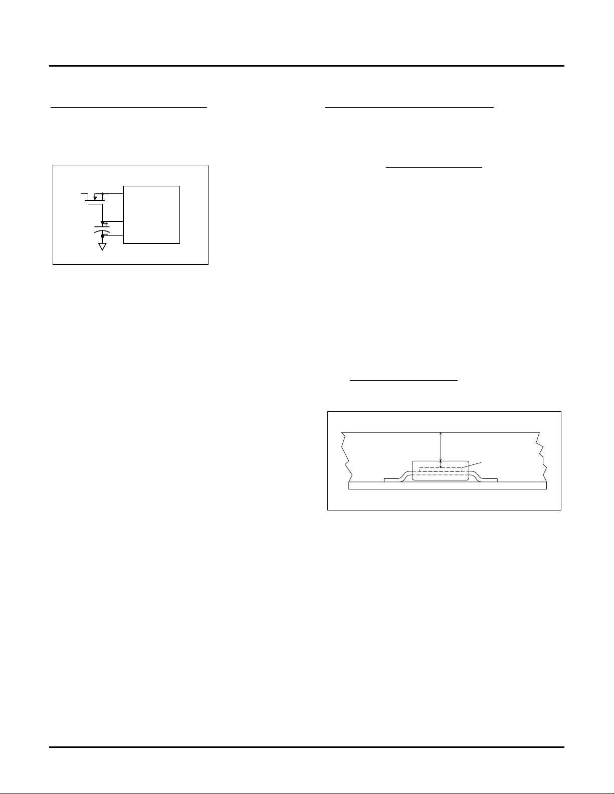
Design Information - continued
Operating from a full wave rectified AC input
For these applications there is no minimum input voltage, thus
adding a fixed value series resistor is not possible. However, a
dynamic resistor consisting of a depletion MOSFET may be added
as depicted in the following diagram.
DN3145N8
Vs
HV9906
1
+Vin
2
Von
3
Vdd
45
AGND
GATE
PGND
NS
PS
This method limits the +V
voltage to VDD + V
IN
depletion MOSFET for all input voltages and in fact raises the
maximum allowable peak input voltage to the breakdown voltage
rating of the depletion MOSFET. The worst-case power
dissipation in the HV9906 is now given by the equation
Power Dissipation HV9906 =
(
and the dissipation in the depletion MOSFET is given by the
equation
Power Dissipation in MOSFET
Which for the previously calculated input current of 3mA, 265V
input voltage and using the DN3145N8 depletion MOSFET yields
the following results.
Power Dissipation HV9906 = (
Power Dissipation in MOSFET
Power Dissipation in MOSFET ≈ 0.76W
8
7
6
of the
GS(OFF)
I)VV ×+
INmax)OFF(GSDD
I)VVV( ×−−≈
IN)OFF(GSDDS
RMS
3
−
=××+
mW5.43103)5.311
3
−
103)5.110265(
××−−≈
HV9906
Using High Thermal Conductivity Encapsulation
For an encapsulated application the required thermal resistance of
the encapsulating material can be calculated using the following
equation.
R
=
ca
θ
θ
IV
×
IN(max)IN
is the required thermal resistance of the encapsulating
R
θca
material.
is the maximum junction temperature.
T
j
is the maximum ambient temperature.
T
a
R
is the junction to case thermal resistance of the package.
θjc
is the maximum DC or RMS input voltage.
V
IN(max)
is the input current required at the highest operating frequency.
I
IN
As an example, consider an application where the input current is
3mA as calculated earlier, operating with a maximum input voltage
of 265V
in an 85°C ambient and an SOIC packaged device will
RMS
be used. The thermal resistance of the encapsulating material can
then be calculated as follows.
3
−
)10326545(85150
R
=
ca
θ
×××−−
3
−
103265
××
High Thermal Conductivity Encapsulant
Printed Circuit Board
R
ca
θ
R
jc
θ
)IVR(TT
××−−
IN(max)INjcaj
W/C76.36
°=
Dice
8 07/23/02
Supertex, Inc. 1235 Bordeaux Drive, Sunnyvale, CA 94089 TEL: (408) 744-0100 FAX: (408) 222-4895 www.supertex.com
Page 9
Application Information
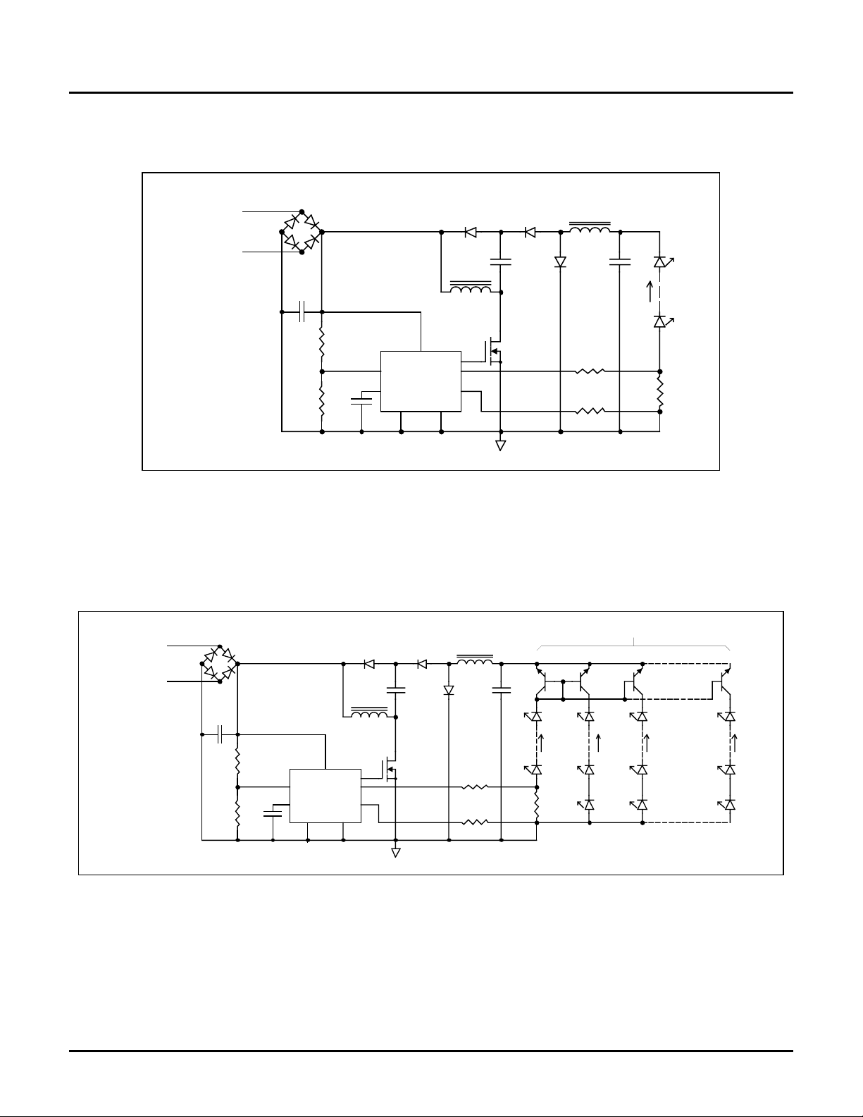
Universal Input Non-Isolated Constant 10mA Average Current LED Lamp Power Supply
1N4007
12VDC to 400VDC
or
65VAC to 280VAC
D1 D2
D4 D3
C1
0.1uF
400V
D5
MURS120T3
C3 C4
0.01uF
L1
1mH
D6
MURS120T3
MURS120T3
L2
220uH
D7
Optional
-
+
10mA
1 to 8
LEDs
HV9906
R1
8M
R2
100k
1uF
to
6.8uF
C2
Von
Vdd
AGND
+Vin
HV9906
U1
GATE
PGND
NS
PS
M1
VN2460N8
R3
700k
R4
200k
This circuit provides a constant average current output, which may
be used to power LED lamps. The circuit maintains a constant
average current and the value of C4 capacitor controls the peak-topeak ripple, which decreases with increasing capacitor value.
If current ripple is permissible then C4 may be omitted.
Universal Input Non-Isolated Constant 0.5A Average Current LED Lamp Power Supply
NPN Bipolar Transistor Array or Matched 2N2222
Q1 Q2 Q3 Q25
-
+
100
LED-1
Row 1
20mA
LED-9
Row 1
R5
LED-1
Row 2
20mA
LED-9
Row 2
LED-10
Row 2
12VDC to 400VDC
or
65VAC to 280VAC
1N4007
D1 D2
D4 D3
C1
0.047uF
400V
R1
8M
R2
100k
1uF
to
6.8uF
D5
MURS160
C3 C4
0.033uF
L1
56uH
U1
+Vin
AGND
HV9906
GATE
PGND
NS
PS
Von
Vdd
C2
D6
MURS160
MURS160
M1
IRFBC30AF
L2
15uH
D7
Optional
R3
900k
R4
300k
R5
250
Negative Voltage
LED-1
Row 3
20mA
LED-9
Row 3
LED-10
Row 3
LED-1
Row 25
20mA
LED-9
Row 25
LED-10
Row 25
This circuit provides 0.5A constant average current output to power
249 LEDs , each operating at 20mA to form a large LED lamp or
array. The circuit maintains a constant average current and the
value of C4 capacitor controls the peak-to-peak ripple, which
decreases with increasing capacitor value.
If current ripple is permissible then C4 may be omitted.
9 07/23/02
Supertex, Inc. 1235 Bordeaux Drive, Sunnyvale, CA 94089 TEL: (408) 744-0100 FAX: (408) 222-4895 www.supertex.com
Page 10
Application Information - continued
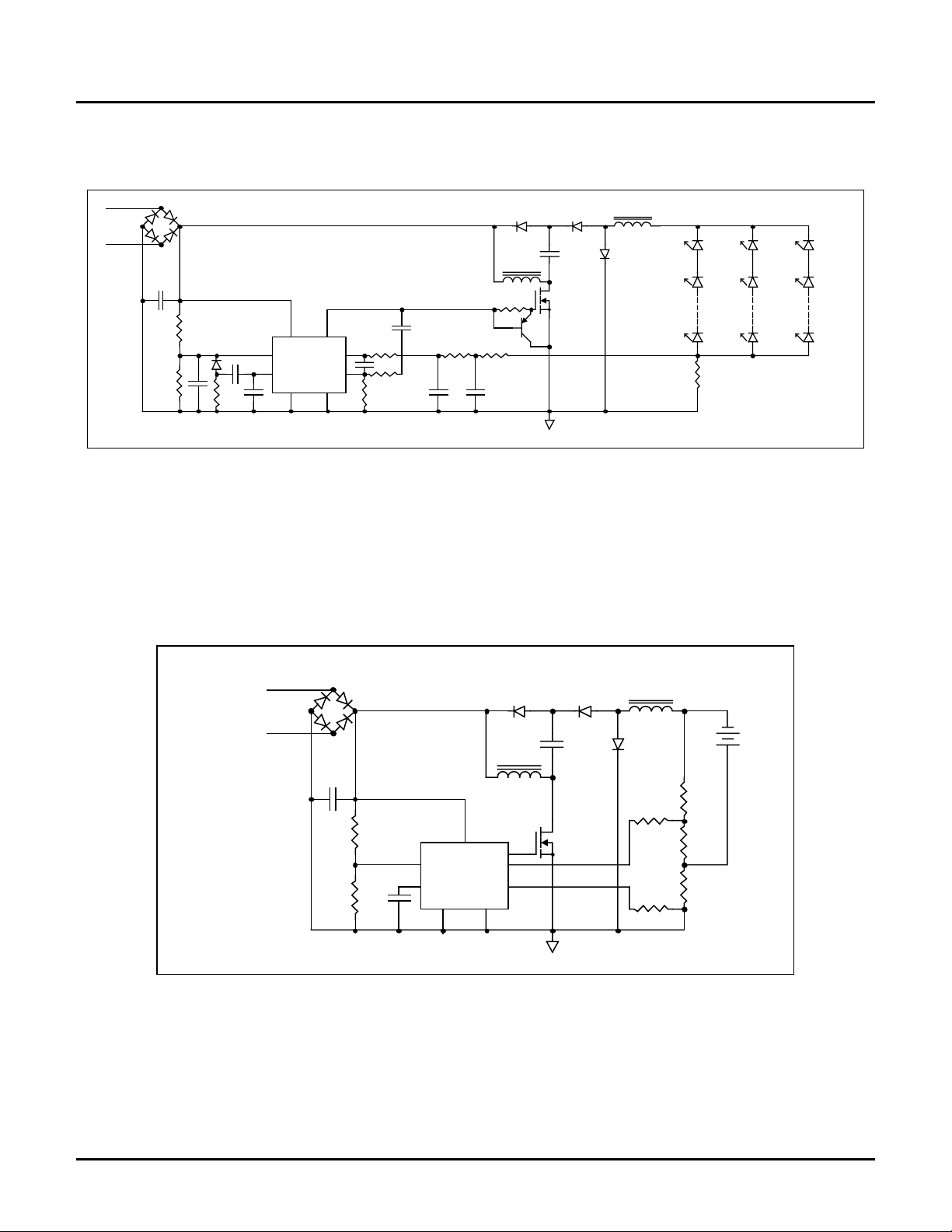
Power Factor Corrected Average Current LED Lamp Power Supply
D1 D2
80VAC
to
135VAC
D4 D3
C1
R10
D6
C9
L1
M1
HV9906
L2
D7
D8
Negative Voltage
LED-1
Row 1
LED-2
Row 1
LED-1
Row 2
LED-2
Row 2
LED-1
Row 3
LED-2
Row 3
R1
C3
D5
R2 R5
C2
R3
C4
Von
Vdd
AGND
U1
HV9906
GATE+Vin
PGND
NS
PS
R4
C6
R6 R8
C5
This power factor corrected circuit provides a constant average
current output to power LED lamps.
12V (6 cell) Lead-Acid Battery Charger
1N4007
D1 D2
12VDC to 400VDC
or
65VAC to 280VAC
D4 D3
C1
0.1uF
400V
R1
8M
Von
Vdd
C2
100k
R1
10uF
AGND
R7
C7 C8
U1
+Vin
HV9906
PGND
Q1
LED-5
Row 1
R9
LED-5
Row 2
It is intended to meet the following specifications:
Input Voltage 80VAC to 135VAC
LED String Forward Voltage 20V
Power Factor >0.95
THD <15%
P 10W
MURS120T3
GATE
NS
PS
D5
C3
L1
D6
MURS120T3
MURS120T3
M1
L2
12V
D7
R5
R3
225k
150k
13.3k
R6
500
R7
R4
0.5
+
Lead-Acid
Battery
LED-5
Row 3
This floating battery charger circuit will charge a 6 cell 12V leadacid battery to a float voltage of 13.8V and provides a 1A charging
current limit for a severely discharged or shorted battery.
When the discharged battery terminal voltage is at 12V, the
charging current is 130mA. The charging current decreases as the
battery charges and the terminal voltage rises. When the
maximum float voltage of 13.8V is reached the current into the
battery will be essentially zero.
10 07/23/02
Supertex, Inc. 1235 Bordeaux Drive, Sunnyvale, CA 94089 TEL: (408) 744-0100 FAX: (408) 222-4895 www.supertex.com
 Loading...