

Page 1
HV9904 Multi Converter Controller
Features
Eliminates High Voltage Input Electrolytic Capacitor
Smallest and Most Reliable Off-Line Solution
Constant Current or Constant Voltage Mode Control
Can be Operated Directly from Rectified AC Mains
10V to 400V Input Range Internal Regulator
1.5mA Operating Supply Current
PLL Based Loop Control with Soft Start
On-Time Varies Inversely with Input Voltage
Frequency Varies with Load
2.5V Differential Sense
Recommended for <10W Applications
Applications
Universal Input Voltage LED driver
Constant Current Source
Battery Charger
Ordering Information
Package Options
8 Pin Plastic DIP 8 Pin SOIC Dice
HV9904P HV9904LG HV9904X
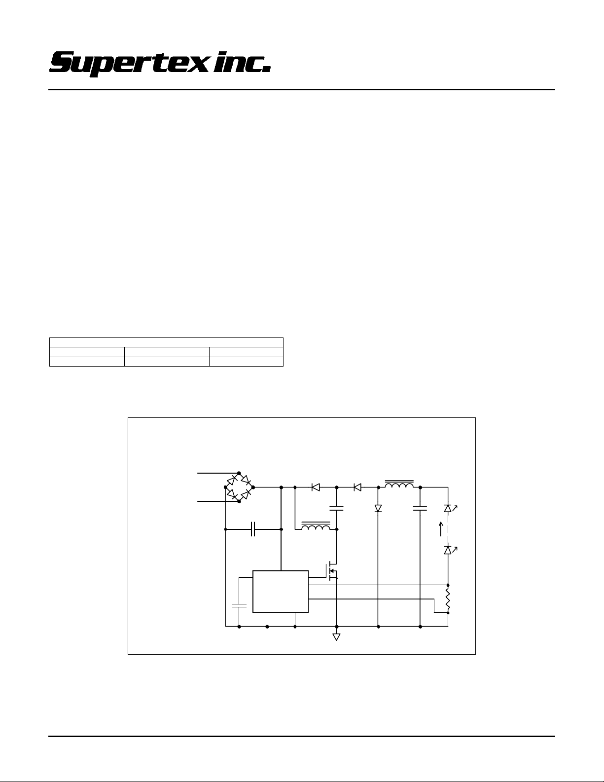
Typical Application Circuit
HV9904
Preliminary Engineering Specification
General Description
The Supertex HV9904 is a second order PWM controller designed
to provide a constant average current output or a constant average
voltage output from an input of 10V to 400V DC or directly from
rectified AC mains up to 280V. The second order topology is
capable of extremely high dynamic control range, allowing
operation directly from rectified AC mains without the need for
bulky and expensive high voltage input electrolytic capacitor.
The PWM control utilizes feed forward circuitry to compensate for
large variations in input voltage (i.e. rectified AC) and a novel
integrator lock loop PLL scheme to regulate a differentially sensed
feedback node where the signal may be discontinuous. This
feedback node could be a current sense resistor or divider from
regulated output voltage. For a constant load the switching
frequency will be nearly constant with a dither of a few kHz helping
to meet FCC conducted emissions requirements.
A high input voltage linear regulator provides a stable Vdd supply
for the internal circuitry and gate drive to the external MOSFET.
Under voltage lockout provides a power on reset and protection for
the MOSFET
Universal Input Constant Average Currrent LED Lamp Power Supply
1N4007
10VDC to 400VDC
or
VAC to 265V
D1 D2
D4 D3
C2
1uF
C1
0.1uF
400V
Vdd
AGND
+Vin
HV9904
U1
GATE
PGND
D5
MURS120T3
0.01uF
1mH
NS
PS
MURS120T3
C3 C4
MURS120T3
L1
VN2460N8
or
M1
IRFBC30AS
D6
L2
220uH
D7
0.1uF
1 to 8
10mA
LEDs
R1
250
Prepare by Telecom Group 1 Rev. D 3/29/2002
Supertex, Inc. 1235 Bordeaux Drive, Sunnyvale, CA 94089 TEL: (408) 744-0100 FAX: (408) 222-4895 www.supertex.com
Page 2
HV9904
Electrical Characteristics
Symbol Parameter Min Typ Max Units Conditions
Input Regulator/Vdd Supply
+V
IN
+I
IN
V
DD(REG)
V
DD(RIPPLE)
UVLO Under Voltage Lockout Threshold 8 V
UVLO Under Voltage Lockout Hysteresis 0.5 V
Regulator Input Voltage 10 400 V
Input Current 1.5 mA
Regulator Output Voltage 10 V
Maximum Ripple Voltage 1 V(P-P)
MOSFET Gate Drive Output
t
R
t
F
Rise Time 75 nSec C
Fall Time 75 nSec C
PWM
P
MIN
P
MAX
f
Minimum Output Frequency 10 kHz +VIN = 15V, VPS = 0V, VNS = -4V
MIN
Minimum Output Pulse Width 200 300 nSec +VIN = 400V
Maximum Output Pulse Width 2 uSec +VIN = 15V
Current Sense
VPS - VNS Current Sense Voltage 2.3 2.5 2.7 V -5V w VPS w 0V, -5V w VNS w 0V
Absolute Maximum Ratings*
+V
Input Voltage -0.3V to +450V
IN
Operating Ambient Temperature Range -40°C to +85°C
Operating Junction Temperature Range -40°C to +125°C
Storage Temperature Range -65° C to +150°C
Power Dissipation @ 25°C, SOIC 750mW
Power Dissipation @ 25°C, Plastic DIP 750mW
*All vol tages referenced to AGND and PGND connec ted together.
(-40°C w TA w +85°C)
= 750pF
OUT
= 750pF
OUT
Prepare by Telecom Group 2 Rev. D 3/29/2002
Supertex, Inc. 1235 Bordeaux Drive, Sunnyvale, CA 94089 TEL: (408) 744-0100 FAX: (408) 222-4895 www.supertex.com
Page 3
HV9904
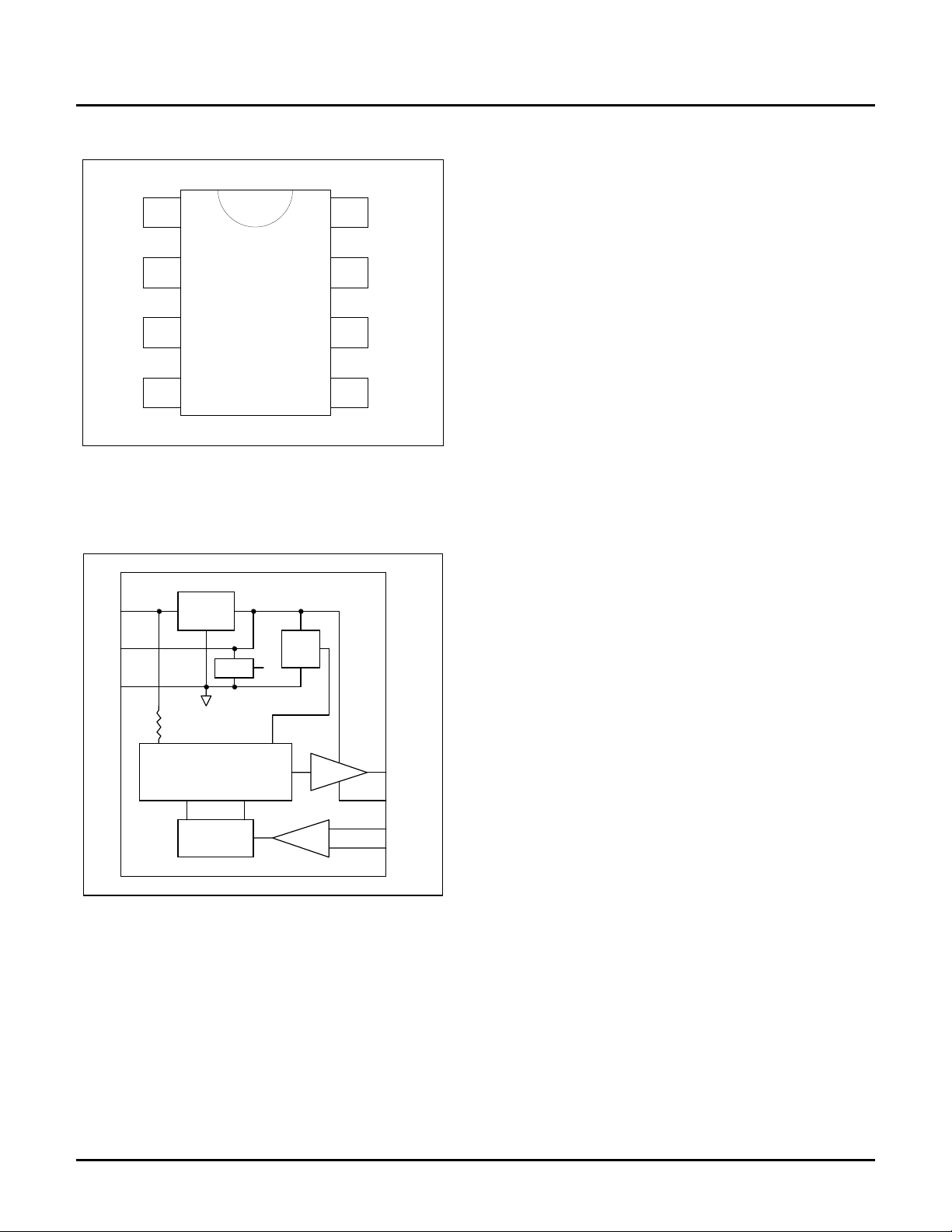
Pinout
+Vin
1
NC PGND
2
GATE
8
7
HV9904
Vdd
3
AGND PS
4
NS
6
5
__________________________________________________________________________________________________________________
Functional Block Diagram
Reference
Vdd
Vref
UVLO
Differential
Sense
Gate
Driver
GATE
PGND
PS
NS
+Vin
Vdd
AGND
Regulator
Variable Frequency and
Duty Cycle Oscillator
Integrator
Functional Description
On initial power application the high input voltage (10V to 400V)
linear regulator charges the capacitor connected to Vdd and seeks
to provide a stable supply for the internal circuitry and gate drive to
the external MOSFET. Under voltage lockout (UVLO) holds the
oscillator disabled and reset to its lowest frequency state until the
Vdd supply rises above 8Volts assuring sufficient gate drive
voltage for the external MOSFET. Once Vdd is above the UVLO
threshold the oscillator is enabled and the external MOSFET is
driven via the gate driver at the oscillator frequency. The UVLO
has a 0.5V hysteresis to prevent false triggering due to ripple on
Vdd.
Pin Description
+V
–
This is the input to the internal linear regulator that provides
IN
the constant voltage VDD internal supply for the PWM. It can
accept DC input voltages in the range of 10 to 400 Volts.
–
V
This is the output of the internal linear regulator and the
DD
supply pin for the PWM circuits. It must be bypassed with a
capacitor capable of storing sufficient energy so that the voltage
does not decay below the UVLO threshold during the time when
the input voltage is below the minimum required by the regulator.
NC –
No internal connection to this pin.
AGRD –
Common connection for analog circuits.
GATE –
This is the PWM output for driving the gate of an N-
channel external MOSFET.
PGRD –
Common connection for GATE drive circuit.
NS –
This is negative sense input to the PWM control circuit.
PS –
This is positive sense input to the PWM control circuit
The duty cycle of the oscillator output and thus the on time of the
MOSFET is determined by a feed forward circuit that sets the
maximum on time based on the instantaneous value of the input
voltage, thus avoiding core saturation of the magnetic elements.
The oscillator is initially operating at its lowest frequency and
continues to operate at this low frequency for several cycles to
assure that a stable equilibrium state is reached. After this initial
delay the feedback circuit is enabled and the oscillator frequency is
increased in small steps on oscillator cycles until the PWM output
(current or voltage) reaches the programmed value. Since the rate
of increase in frequency is a function of the frequency the oscillator
frequency will rise exponentially.
The differential sense circuit monitors the programming node
(voltage on current sense resistor for constant average current
control or voltage on resistive divider for constant average voltage
control) using an integrator lock loop feedback to obtain a stable
average value from even a discontinuous signal. As long as this
average value is less than 2.5V the oscillator frequency is
incremented. When the average value reaches 2.5V the oscillator
frequency incrementing is halted. If the average value exceeds
2.5V then the oscillator frequency is decremented. In this manner
the oscillator frequency is dithered to maintain output regulation
while the feed forward sensing of the input voltage maintains a
fixed value of energy transfer per oscillator cycle.
Line regulation is controlled by the instantaneous feed forward
sensing of the input voltage, thus the PWM can easily track a full
wave rectified sine wave of input voltage at 50Hz, 60Hz or 400Hz
provided that the capacitor connected at Vdd can store sufficient
energy to prevent decay below the UVLO threshold during the time
when the resulting input voltage at +Vin is below 10V. For a 50Hz
rectified sine wave a 1µF capacitor connected to Vdd is sufficient
to guarantee stable operation at 50Hz.
Load regulation is controlled via the feedback sensing circuit by
adjusting the oscillator frequency to maintain average energy
transfer consistent with the load conditions. For relatively stable
load conditions this method achieves excellent regulation. For a
constant load the switching frequency will be nearly constant with a
dither of a few kHz helping to meet FCC conducted emissions
requirements.
Prepare by Telecom Group 3 Rev. D 3/29/2002
Supertex, Inc. 1235 Bordeaux Drive, Sunnyvale, CA 94089 TEL: (408) 744-0100 FAX: (408) 222-4895 www.supertex.com
Page 4
Application Information
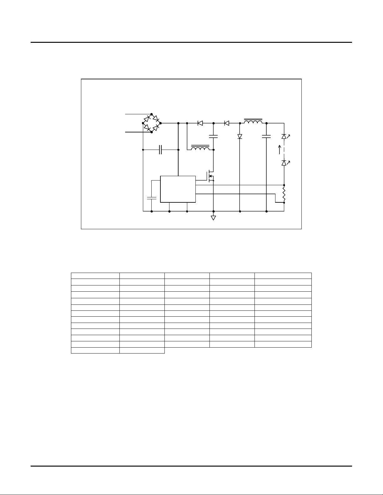
Non-Isolated Constant Current Output PWM
Universal Input Constant Average Currrent LED Lamp Power Supply
1N4007
D1 D2
10VDC to 400VDC
or
VAC to 265V
D4 D3
C1
0.1uF
400V
C2
1uF
Vdd
AGND
+Vin
HV9904
U1
GATE
PGND
D5
MURS120T3
0.01uF
1mH
NS
PS
MURS120T3
C3 C4
MURS120T3
L1
VN2460N8
or
M1
IRFBC30AS
HV9904
D6
L2
220uH
D7
0.1uF
1 to 8
10mA
LEDs
R1
250
This circuit provides a constant average current output, which may
be used to power LED lamps. The circuit maintains a constant
average current and the value of C4 capacitor controls the peak-topeak ripple, which decreases with increasing capacitor value. If
Item Number Quantity Reference Value Manufacturer
1 1 C1
2 1 C2
3 1 C3
4 1 C4
5 4 D1, D2, D3, D4 1N4007 On Semiconductor
6 3 D5, D6, D7 MURS120T3 On Semiconductor
7 1 L1 DO1608C-105 Coilcraft
8 1 L2 DO1608C-224 Coilcraft
9 1 M1 VN2460N8 Supertex
10 1 R1
11 1 U1 HV9904LG Supertex
Total Part Count 16
very high current ripple values are permissible then C4 may be
omitted. The following BOM provides a list of suggested
components.
0.1µF, 500V
1µF, 15V
0.01µF, 500V
0.1µF,25V
250Ω
Vishay
Vishay
Vishay
Vishay
Prepare by Telecom Group 4 Rev. D 3/29/2002
Supertex, Inc. 1235 Bordeaux Drive, Sunnyvale, CA 94089 TEL: (408) 744-0100 FAX: (408) 222-4895 www.supertex.com
Page 5
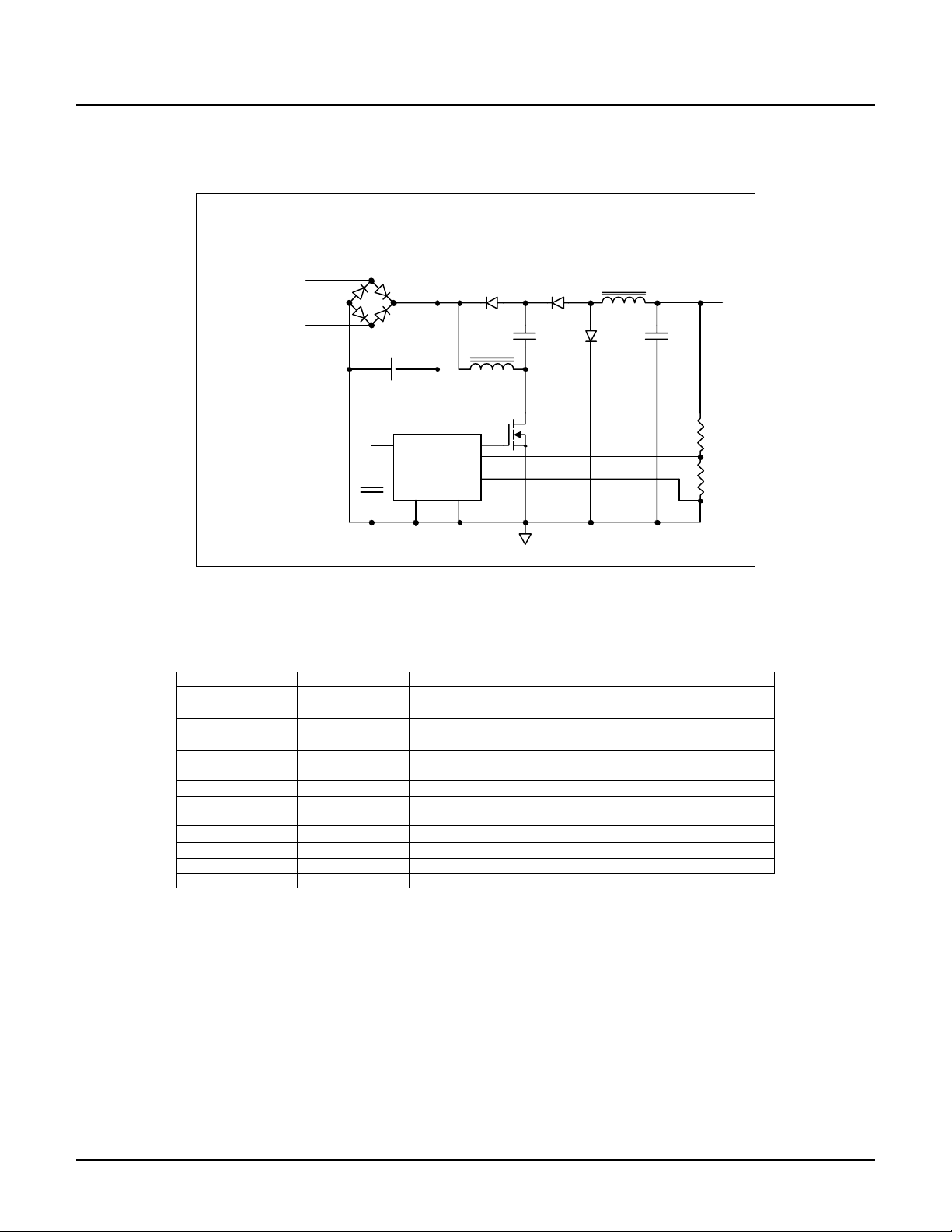
Application Information - Continued
Non-Isolated Constant Voltage Output PWM
Universal Input Power Supply
1N4007
D1 D2
10VDC to 400VDC
or
VAC to 265VAC
D4 D3
HV9904
D5
MURS120T3
0.01uF
MURS120T3
C3 C4
MURS120T3
D6
L2
220uH
-5V
D7
100uF
C1
0.1uF
400V
Vdd
C2
1uF
HV9904
AGND
This circuit provides a non-isolated constant voltage output. The
value of C4 capacitor controls the peak-to-peak ripple, which
Item Number Quantity Reference Value Manufacturer
1 1 C1
2 1 C2
3 1 C3
4 1 C4
5 4 D1, D2, D3, D4 1N4007 On Semiconductor
6 3 D5, D6, D7 MURS120T3 On Semiconductor
7 1 L1 DO1608C-105 Coilcraft
8 1 L2 DO1608C-224 Coilcraft
9 1 M1 VN2460N8 Supertex
10 1 R1
11 1 R2
12 1 U1 HV9904LG Supertex
Total Part Count 17
L1
1mH
+Vin
U1
GATE
PGND
NS
PS
M1
VN2460N8
or
IRFBC30AS
R2
25k
R1
25k
decreases with increasing capacitor value. The following BOM
provides a list of suggested components.
0.1µF, 500V
1µF, 15V
0.01µF, 500V
100µF, 6.3V
25kΩ
25kΩ
Vishay
Vishay
Vishay
Panasonic
Prepare by Telecom Group 5 Rev. D 3/29/2002
Supertex, Inc. 1235 Bordeaux Drive, Sunnyvale, CA 94089 TEL: (408) 744-0100 FAX: (408) 222-4895 www.supertex.com
 Loading...