

Page 1
Features
Operating voltage: 2V~12V
·
Low power consumption
·
Built-in oscillator needs only 5% resistor
·
0/2/4/8 data selectable
·
224maximum address and data codes
·
Easy interface with an RF or IR medium
·
Applications
Burglar alarm system
·
Smoke and fire alarm system
·
Garage door controllers
·
Car door controllers
·
General Description
The HT6P20 is a CMOS LSI encoder designed
for remote control system applications. It en
codes 24 bits of information and then serially
transmits it via the DOUT pin upon receipt of
transmission enable (DATA pins: D0~D7) signals. The combination of address and data bits
of the HT6P20 is designed using one time pro-
HT6P20
24
2
One time programmable process
·
Data active: D0~D7
·
Minimal external components
·
HT6P20/A/B: 8-pin DIP/NSOP package
·
HT6P20/D: 16-pin DIP/NSOP package
Security system
·
Cordless telephones
·
Other remote control systems
·
grammable process. In addition, the chip offers
various packaging for flexible combination of
programmable address/data so as to meet vari
ous applications. Its programmable ad
dress/data is transmitted together with the
anti-code bits via RF or infrared transmission
medium upon receipt of a trigger signal.
OTP Encoder
-
-
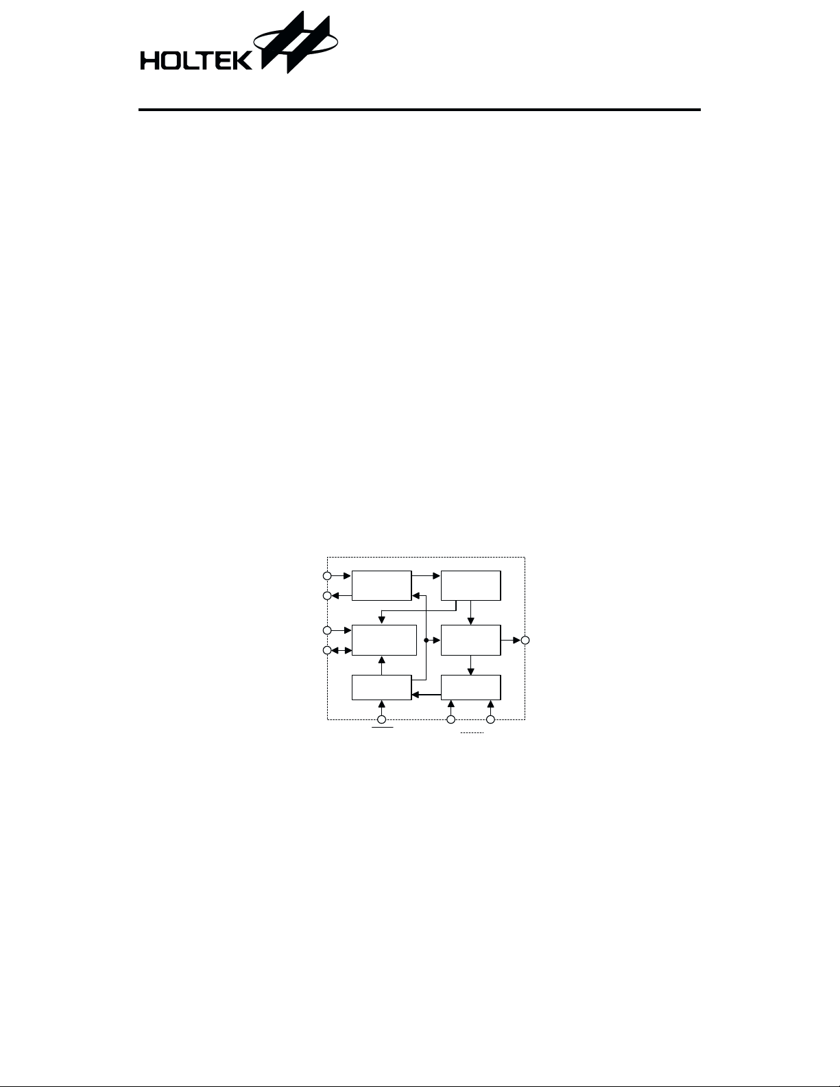
Block Diagram
OSC1
OSC2
VPP
SIO
Note: Address/Data numbers are available in various combinations, refer to the functional descrip
tion.
Oscillator
Program m ing
Circuit
C ontrol U nit
PGM
Address
C ounter
Mixer &
Driver
D a ta L a tc h
D0 D7
1 May 2, 2000
DOUT
Page 2
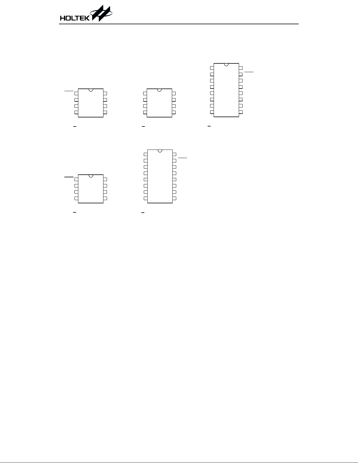
Pin Assignment
HT6P20
24-A ddress
0 -D a ta
PGM
1
VSS
2
OSC2
3
OSC1
4
H T6P 20A
8 D IP /N S O P
SIO
8
VPP
7
VDD
6
DOUT
5
22-A ddress
2 -D a ta
D0
1
D1
2
VSS
3
OSC2
4
HT6P20B
8 D IP /N S O P
B lank device B lank device
D1
1
PGM
VSS
OSC2
OSC1
1
2
3
4
8
7
6
5
HT6P20
8 D IP /N S O P
SIO
VPP
VDD
DOUT
D2/NC
D3/NC
D4/NC
D5/NC
D6/NC
D7/NC
2
3
VSS
4
5
6
7
8
HT6P20
1 6 D IP /N S O P
20-A ddress
4 -D a ta
D1
D2
D3
VSS
NC
8
VDD
7
DOUT
6
OSC1
5
NC
NC
NC
NC
16
1
2
3
4
5
6
7
8
D0
15
PGM
14
SIO
13
VPP
12
VDD
11
DOUT
10
OSC1
9
OSC2
HT6P20D
1 6 D IP /N S O P
D0
16
PGM
15
SIO
14
VPP
13
VDD
12
DOUT
11
OSC1
10
OSC2
9
Note:
The customer code and control code have been programmed into HT6P20A/B/D by Holtek¢s
factory process.
The blank device HT6P20 is not programmed, it can be programmed by Holtek¢s programming
kit.
Warning: The 8-pin blank device only allows programming as HT6P20A type.
The 16-pin blank device allows programming as one of HT6P20/D type. After program
ming the HT6P20 pin name are the same as one of HT6P20D, which is determined by the
kit programming procedure.
Pin name ²NC² stands for no connection (floating).
2 May 2, 2000
-
Page 3
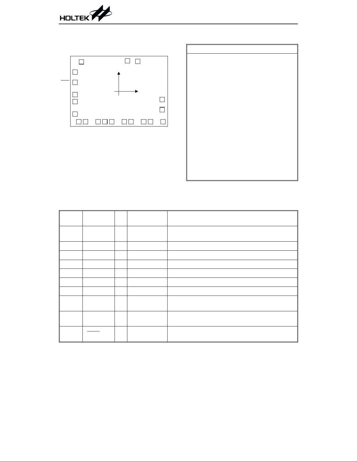
HT6P20
Pad Assignment Pad Coordinates
DOUT
NC
VDD
20
(0 ,0 )
12 13
D4
D5
19
14 15
D6
NC
18
17
16
OSC1
OSC2
D7
Pad No. X Y
1
2
3
4
5
6
7
-1123.00
-1123.00
-1123.00 -86.25
-1123.00 -261.25
-1123.00 -583.75
-1027.50 -776.75
8
9
10
11
12 142.50
SIO
PGM
D0
NC
D1
2
3
4
5
6
VPP
1
7 8
D2
D3
9 10 11
VSS
NC
13 317.50
14 640.00
Chip size: 2590 ´ 2010 (mm)
2
* The IC substrate should be connected to VSS in
the PCB layout artwork.
15 815.00
16 1137.50
17 1118.00
18 1118.00
19 489.00 772.05
20 223.50 789.75
Pin Description
HT6P20D
Pin No. Pin Name I/O
16
1~3
4 VSS
5~8 NC
D0~D3 I
¾¾
¾¾
9 OSC2 O OSCILLATOR Oscillator output pin
10 OSC1 I OSCILLATOR Oscillator input pin
11 DOUT O CMOS OUT Data serial transmission output
12 VDD
¾¾
13 VPP I
14 SIO I/O
15 PGM
Connection
I
Internal
CMOS IN
Pull-high
¾
CMOS
IN/OUT
CMOS IN
Pull-high
Description
Data input and transmission enable (active low)
They can be externally set to VSS or left open.
Negative power supply, ground
No connection
Positive power supply
Programming power supply, V
tion
Programming address/control code input and mode
code output for mode verification
Program mode control pin, active low
Unit: mm
-956.50
762.75
498.75
236.25
-852.50 -776.75
-530.00 -776.75
-355.00 -776.75
-180.00 -776.75
-776.75
-776.75
-776.75
-776.75
-776.75
-466.75
-205.75
for normal opera
DD
-
3 May 2, 2000
Page 4

Approximate internal connection circuits
HT6P20
CMOS IN/O UT
CMOS OUT
CMOS IN
Pull-high
V
DD
OSC1
OSCILLATOR
OSC2
Absolute Maximum Ratings
Supply Voltage ..............................-0.3V to 12V
Input Voltage .................V
-0.3V to VDD+0.3V
SS
Note: These are stress ratings only. Stresses exceeding the range specified under ²Absolute Maxi
mum Ratings² may cause substantial damage to the device. Functional operation of this de
vice at other conditions beyond those listed in the specification is not implied and prolonged
exposure to extreme conditions may affect device reliability.
Electrical Characteristics
Symbol Parameter
V
DD
I
STB
I
DD
V
IH
V
IL
R
PH
I
DOUT
f
OSC
Operating Voltage
Standby Current 12V Oscillator stops
Operating Current 12V
²H² Input Voltage ¾¾
²L² Input Voltage ¾¾
D0~D7 Pull-high Resistance 12V
Output Current
Oscillator Frequency 12V
Source
Sink
V
DD
¾¾
5V
12V
5V
12V
Storage Temperature.................-50°Cto125°C
Operating Temperature ..............-20°Cto75°C
Test Conditions
Min. Typ. Max. Unit
Conditions
No load
f
=3kHz
OSC
0.8V
¾¾
0.9V
DD
0.9V
DD
0.1V
DD
0.1V
DD
=1.4MW¾
R
OSC
2
¾
¾
0
-2 -5 ¾
-6.5 -15 ¾
25
615
¾
12
200 400
¾
DD
¾
150 300
3
12 V
V
DD
0.2V
DD
¾
¾
¾
Ta=25°C
mA
mA
V
V
kW
mA
mA
mA
mA
kHz
-
-
4 May 2, 2000
Page 5

Functional Description
HT6P20
Programming
The HT6P20 is a one time programmable encod
ing integrated circuit. The programmable codes
consist of 4-bit control codes and 24-bit address
codes. Before using the device, first program the
internal 4 control bits and 24 address bits. Then,
to program the address and control codes, con
nect the PGM
pin to VSS, allowing the SIO pin to
receive control and address codes from the con
tinuously transmitting programming kit. The
control codes (B0~B3) and address timing are re
spectively shown on the Table and the Figure for
Programming Timing. In the programming pro
cess, the mode bit (B0) has to be programmed
first. The 0/2/4/8 data number is selected by the
address along with the data format bits (B1,B2).
The HT6P20, in addition, provides a polarity bit
(B3) to select the polarity of the output data.
Various packages of the HT6P20 offer program
mable combinations of address/data to meet
various application needs.
B1 B2 B3
B0
P o la rity c o n tro l
Address and data form at
M ode control
Table 1: Control code
-
·
Mode control (B0)
B0 Function
0 Not programmed
-
-
-
1 Programmed
·
Address and data format (B1,B2)
B2 B1 Code Format
0 0 A0~A23
0 1 A0~A21 + D1~D0
1 0 A0~A19 + D3~D0
1 1 A0~A15 + D7~D0
·
-
Polarity control (B3)
B3 Data Output Polarity
0 Negative polarity
1 Positive polarity
The HT6P20A/D can be programmed by the
SIO pins. The HT6P20B, on the other hand, is
programmed for 2-data and positive polarity
application.
Programming timing of the HT6P20D (B0~B3=1010)
OSC2
(3kH z)
PGM
SIO
0
1
1
0
0
100 10
(2 ) A 0 ~ A 2 3 a re a d d r e s s c o d e s
(3) A20 ~ A 23 stands for don't care for the H T6P 20D
(4) SIO m ust be set to "H igh" during C and B 0 periods
(5 ) 0 : " L o w "; 1 : "H ig h " ; X : D o n 't c a re
Program m ing
bit
1
B0 B1 B2 B3 A0 A1 A2 A3 A18 A19A20 A21A22 A23
C
Program m ing
N o te : (1 ) B 0 ~ B 3 a re c o n tr o l c o d e s
Programming timing for the HT6P20D
5 May 2, 2000
X
X
X
X
Page 6

HT6P20
Normal operation
The HT6P20 encodes and transmits address/data to a decoder upon receipt of a trigger signal. The
address codes of the HT6P20A are always transmitted as long as power (VDD) is supplied. The trans
mission function of the HT6P20B/D is enabled by the D0~D7 pins (active low). The following is the
transmission timing of the HT6P20:
D 0 ~ D 7
Encoder
DOUT
< 1 w ord
Transmission timing
A complete code word of the HT6P20D consists of 3 periods as shown below.
fo s c
DOUT
1 c lo c k
p ilo t p e r io d
(23 clocks)
1 /3 b it
(A 0~ A 1 9, 60 clocks)
address code period
A complete code word for the HT6P20D
The HT6P20A/B/D detects the logic state of the internal programmed address and the external data
pins, and then transmits the detected information during the code period. Each address/data bit can be
set to one of the following two logic states:
> 1 w ord
(D 3 ~D 0 , 12 clo cks)
data code period
0011
anti-code period
(4 b its )
-
fo sc
" O ne"
"Z ero"
Address/
Data bit
6 May 2, 2000
Page 7

Flowchart
HT6P20
Power on
Standby m ode
No
No
Application Circuits
Transm itter C ircuit
1
PGM
2
Rosc
3
4
VSS
OSC2
OSC1
VPP
VDD
DOUT
Transm ission
enabled ?
Address/data w ords
transm itted
Transm ission
still enabled
Address/data w ords
transm itted
continuously
8
SIO
7
6
TE
5
Yes
Yes
LED
+12V
No
No
N ote: O ne tim e program m able
PGM =0 ?
Yes
Program m ing
m ode
Program m ing
com pleted ?
Yes
Transm itter C ircuit
1
2
3
4
5
6
7
8
D2
D3
VSS
NC
NC
NC
NC
D0D1
PGM
SIO
VPP
VDD
DOUT
OSC1
OSC2
16
15
14
13
12
11
10
9
+12V
LED
Rosc
HT6P20A
Rosc@1 .4 M
HT6P20D
W
Rosc@1 .4 M
7 May 2, 2000
W
Page 8

Transm itter C ircuit
HT6P20
1
2
D2
3
D3
4
VSS
5
NC
6
NC
7
NC
8
NC
HT6P20D
Rosc@1 .4 M
16
D0D1
15
PGM
14
SIO
13
VPP
12
VDD
11
DOUT
10
OSC1
9
OSC2
W
Transm itter Circuit
1
2
D2
D3
VSS
NC
NC
NC
NC
HT6P20D
Rosc@1 .4 M
PGM
VPP
VDD
DOUT
OSC1
OSC2
3
4
5
6
7
8
Rosc
D0D1
SIO
+12V
100
W
0.1mF
+12V
100k
W
4.7k
W
16
15
14
13
12
11
10
Rosc
9
100
0.1mF
+12V
W
LED
Transm itter Circuit
1
2
D2
D3
VSS
NC
NC
NC
NC
PGM
VPP
VDD
DOUT
OSC1
OSC2
3
4
5
6
7
8
SIO
16
D0D1
15
14
13
100
Rosc
0.1mF
W
LED
12
11
10
9
HT6P20D
W
Rosc@1 .4 M
W
Note:
In order to prevent the IC from getting damaged due to the latch up, the 100W resistor or the
LED which can also be a transmission indicator is indispensible when V
=9V~12V.
DD
8 May 2, 2000
Page 9

HT6P20
Holtek Semiconductor Inc. (Headquarters)
No.3 Creation Rd. II, Science-based Industrial Park, Hsinchu, Taiwan, R.O.C.
Tel: 886-3-563-1999
Fax: 886-3-563-1189
Holtek Semiconductor Inc. (Taipei Office)
5F, No.576, Sec.7 Chung Hsiao E. Rd., Taipei, Taiwan, R.O.C.
Tel: 886-2-2782-9635
Fax: 886-2-2782-9636
Fax: 886-2-2782-7128 (International sales hotline)
Holtek Semiconductor (Hong Kong) Ltd.
RM.711, Tower 2, Cheung Sha Wan Plaza, 833 Cheung Sha Wan Rd., Kowloon, Hong Kong
Tel: 852-2-745-8288
Fax: 852-2-742-8657
Copyright Ó 2000 by HOLTEK SEMICONDUCTOR INC.
The information appearing in this Data Sheet is believed to be accurate at the time of publication. However, Holtek
assumes no responsibility arising from the use of the specifications described. The applicationsmentioned herein are
used solely for the purpose of illustration and Holtek makes no warranty or representation that such applications
will be suitable without further modification, nor recommends the use of its products for application that may pres
ent a risk to human life due to malfunction or otherwise. Holtek reserves the right to alter its products without prior
notification. For the most up-to-date information, please visit our web site at http://www.holtek.com.tw.
9 May 2, 2000
-
 Loading...